Bhushan B. Handbook of Micro/Nano Tribology, Second Edition
Подождите немного. Документ загружается.

© 1999 by CRC Press LLC
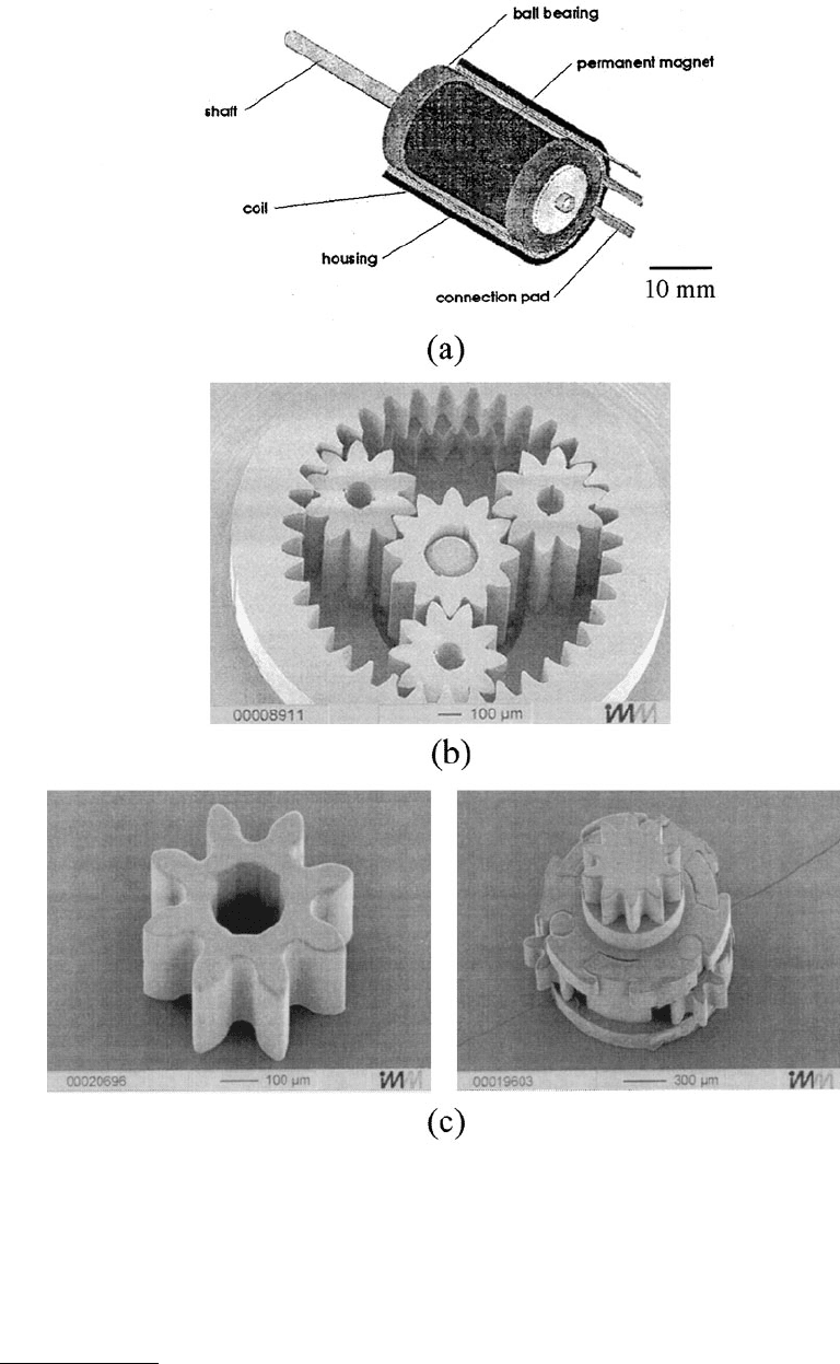
FIGURE 16.8
Schematics of (a) permanent magnet millimotor with integrated milligear box, (b) of wolfrom-type
system made of Ni–Fe metal (Lehr et al., 1996), and (c) of multistage planetary gear system made with microinjected
POM plastic showing a single gear and the gear system. (From Thurigen, C. et al., 1998, in
Tribology Issues and
Opportunities in MEMS,
B. Bhushan, ed., Kluwer Academic, Dordrecht. With permission.)
© 1999 by CRC Press LLC
For the scratch and wear tests, specially fabricated diamond microtips were used (Bhushan et al., 1997a;
Sundararajan and Bhushan, 1998). These microtips consisted of single-crystal natural diamond, ground
to the shape of a three-sided pyramid, with an apex angle of 60° and tip radius of about 70 nm, mounted
on a platinum-coated stainless steel cantilever beam whose stiffness was 50 N/m. Samples were scanned
orthogonal to the long axis of the cantilever with loads ranging from 20 to 100 µN to generate scratch/wear
marks. Scratch tests consisted of generating scratches in a reciprocating mode at a given load for 10 cycles
over a scan length (stroke length) of 5 µm at 10 µm/s. Wear marks were generated over a scan area of
2
×
2 µm at 4 µm/s and the wear marks were observed by scanning a larger 4
×
4 µm area with the wear
mark at the center. Imaging scans of both scratch and wear tests were done at a low normal load of 0.5.
The reported scratch/wear depths are an average of three runs at separate instances. All measurements
were performed in an ambient environment (21 ± 1°C, 45 ± 5% RH).
Hardness and elastic modulus were calculated from load–displacement data obtained by nanoinden-
tation using a commercially available nanoindenter (Bhushan, 1995; Bhushan et al., 1997b; Li and Bhus-
han, 1998). The instrument monitored and recorded dynamic load and displacement of a three-sided
pyramidal diamond (Berkovich) indenter with a force resolution of about 75 nN and displacement
resolution of about 0.1 nm. Multiple loading and unloading were performed to examine reversibility of
the deformation and thereby ensuring that the regime was elastic.
The fracture toughness measurements were made using a microindentation technique. A Vickers
indenter (four-sided diamond pyramid) was used to indent samples in a microhardness tester at a normal
load of 0.5 N. The indentation impressions were examined in an optical microscope to measure the
length of median-radial cracks to calculate the fracture toughness (Li and Bhushan, 1998).
16.2.1.2 Macroscale Tests
Macroscale studies were conducted using either a ball-on-flat tribometer under reciprocating motion or
a magnetic rigid disk drive. In the ball-on-flat tribometer tests, a 5-mm diameter alumina ball (hardness
~ 21 GPa) was slid in a reciprocating mode (2 mm amplitude and 1 Hz frequency) under a normal load
of 1 N in the ambient environment (Gupta et al., 1993). The coefficient of friction was measured during
the tests using a strain gauge ring. Wear volume was measured by measuring the wear depth using a
stylus profiler.
In the magnetic disk drive tests, a modified disk drive was used. The silicon pins or magnetic head
slider specimens to be tested were slid in a unidirectional sliding mode against a magnetic thin-film disk
under a normal load of 0.15 N and the rotational speed of 200 rpm. The sliding speeds at track radii
ranging from 45 to 55 mm varied from 0.9 to 1.2 m/s (Bhushan and Venkatesan, 1993). At these speeds,
the pin or slider specimen remained in contact throughout the period of testing. The coefficient of friction
was measured during the tests using a strain gauge beam. Samples were examined using scanning electron
microscopy to detect any wear. Chemical analyses of the samples were also carried out to study failure
mechanisms.
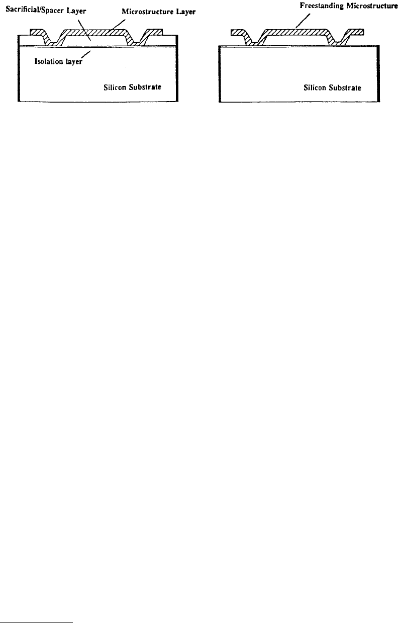
FIGURE 16.9
Schematics of microstructures during fabrication using surface micromachining before and after
removal of sacrificial/spacer layer.

© 1999 by CRC Press LLC
16.2.2 Test Samples
Materials of most interest for planar fabrication processes using silicon as the structural material are
undoped and boron-doped (
p
+
-type) single-crystal silicon and phosphorus-doped (
n
+
-type) LPCVD
polysilicon films. For tribological reasons, silicon needs to be coated with a solid and/or liquid overcoat
or be surface treated, which exhibits low friction and wear.
Studies have been conducted on various types of virgin silicon samples: undoped (lightly doped)
single-crystal Si(100), Si(111), and Si(110) and the following types of treated/coated silicon samples:
PECVD-oxide-coated Si(111), dry-oxidized, wet-oxidized, and C
+
-implanted Si(111) (Bhushan and Ven-
katesan, 1993; Bhushan and Koinkar, 1994). Studies have also been conducted on heavily doped (
p
+
-type)
single-crystal Si(100), undoped polysilicon film, heavily doped (
n
+
-type) polysilicon film and 3C-SiC
(cubic or
β
-SiC) film (Bhushan et al., 1997a,b, 1998; Li and Bhushan, 1998; Sundararajan and Bhushan,
1998). A 10
×
10 mm coupon of each sample was ultrasonically cleaned in methanol for 20 min and
dried with a blast of dry air prior to measurements. The undoped Si(100) was a
p
-type material grown
by the CZ process. It had a boron concentration of 1.7
×
10
15
ions/cm
3
from intrinsic doping during the
manufacturing process. The doped wafer (
p
+
-type single-crystal silicon) was heavily doped with boron
ions (from a solid source of oxide of boron) with concentration of 7
×
10
19
ions/cm
3
down to a depth of
5.5 µm using thermal diffusion. The grain size of polysilicon wafer was about 5 mm. The polysilicon film
was produced as follows: (1) The substrate used was thermally oxidized Si(100) wafers with the oxide
layer grown using a standard wet oxidation recipe to a nominal thickness of about 100 nm; (2) the
polysilicon film was grown on the substrate using an LPCVD process (deposition temperature, 610°C;
silane flow rate, 285 sccm; deposition pressure, 230 mtorr), using the thermal decomposition of silane
vapor. The films were about 3 µm thick, with columnar grains and a grain size of about 750 nm. X-ray
diffraction and transmission electron microscope characterization showed the film to be highly oriented
(110). The
n
+
-doped polysilicon film was obtained by doping the polysilicon film with phosphorus ions
from a solid source of P
2
O
5
by thermal diffusion at 875°C for 90 min. The 3C-SiC films were grown
through an atmospheric pressure chemical vapor deposition (APCVD) process on an Si(100) substrate.
To grow the SiC film on the wafer by carbonizing its surface, the wafer is placed on an SiC-coated graphite
susceptor, which is induction-heated by an RF-generator to the growth temperature of 1360°C in the
presence of propane and silane at 1 atm. Prior to film growth, the wafer is heated to 1000°C in the
presence of hydrogen, which etches the native oxide from the wafer surface (Zorman et al., 1995). The
films obtained were about 2 µm thick. Both as-deposited and polished versions of the undoped polysilicon
and SiC films were studied. The polysilicon film was chemomechanically polished in a Struers Planopol-
3 polishing machine using 100 ml colloidal silica dispersion (Rippey Corporation, particle size of 30 to
100 nm) mixed in 2000 ml deionized water at a force of 210 N for 15 min, with the pads running at
150 rpm in the same direction. The SiC and doped polysilicon films were polished in a Buehler Ecomet-
3 polishing machine with diamond slurry (General Electric Company, particle size of 100 to 500 nm)
for 30 min for SiC and 12 min for doped polysilicon film at a load of 50 N, with the pads running at
10 rpm in the same direction. Doped polysilicon film was polished using Fuji film lapping tape, LT-2,
the main lapping agent being 37-µm-sized Cr
2
O
3
particles.
Boundary lubrication studies have been conducted on silicon samples coated with perfluoropolyether
lubricants (Koinkar and Bhushan, 1996a,b) and Langmuir–Blodgett and chemically grafted self-assem-
bled monolayer films (Bhushan et al., 1995b).
16.3 Results and Discussion
Reviews of five studies are presented in this section. The first study compares micro/nanotribological
properties of various forms of virgin, coated, and treated silicon samples. The second study is composed
of similar studies conducted on SiC film and compares this material to other materials currently used
in MEMS devices. The third study compares the macroscale friction and wear data of virgin, coated, and

© 1999 by CRC Press LLC
treated silicon samples. The fourth study discusses various forms of boundary lubrication that may be
suitable for MEMS devices. Finally, the fifth study presents a review of component level studies.
16.3.1 Micro/nanotribological Studies of Virgin, Coated,
and Treated Silicon Samples
Table 16.2 summarizes the results of the studies conducted on various silicon samples (Bhushan and
Koinkar, 1994). Coefficient of microscale friction values of all the samples are about the same. Table 16.3
compares macroscale and microscale friction values for two of the samples. When measured for small
contact areas and very low loads used in microscale studies, indentation hardness and elastic modulus
are higher than that at the macroscale. This reduces wear. This, added to the effect of the small apparent
area of contact reducing the number of trapped particles on the interface, results in less plowing contri-
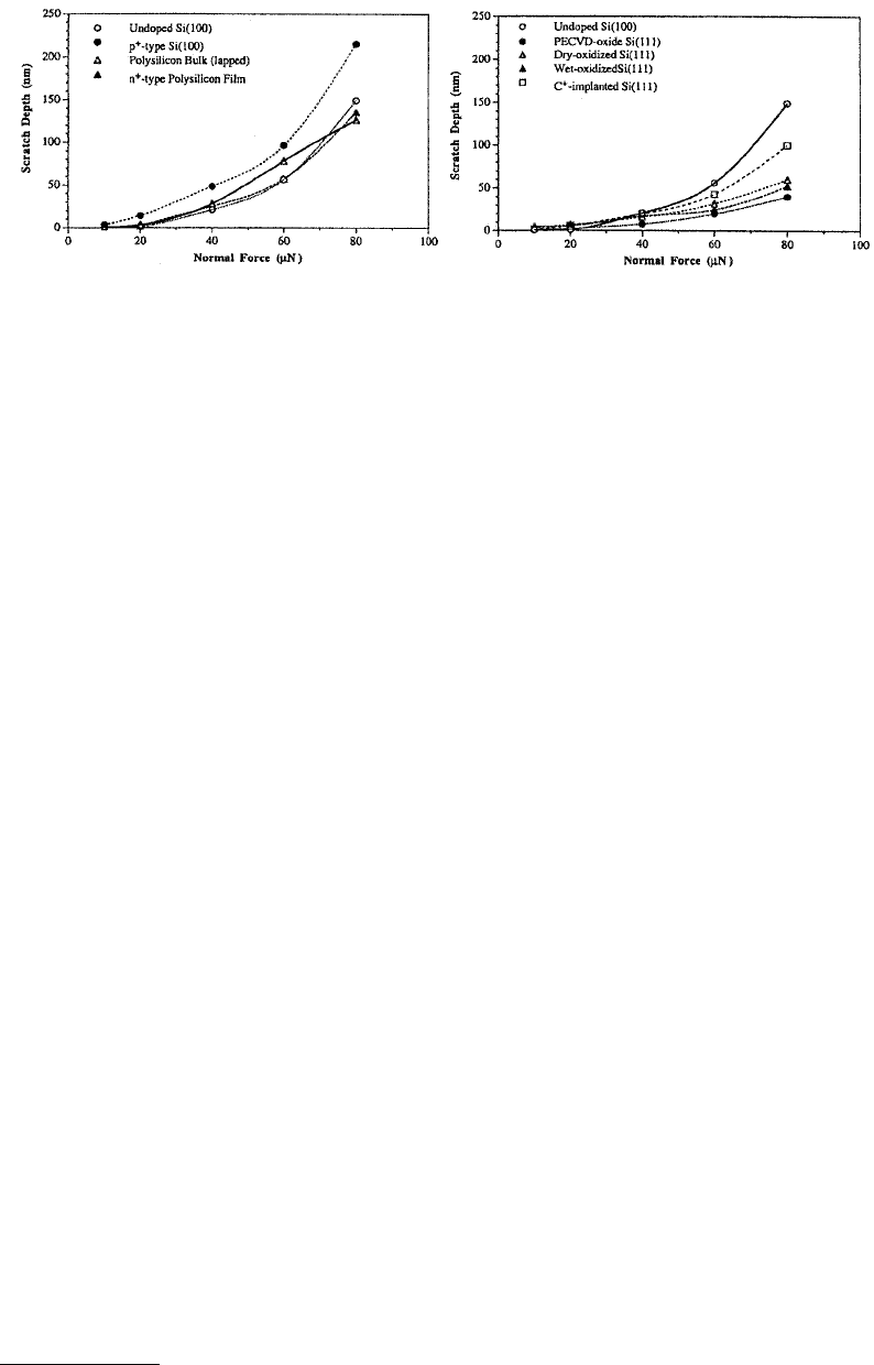
bution in the case of microscale friction measurements. Figure 16.10 and Table 16.2 show microscale
scratch data for the various silicon samples (Bhushan and Koinkar, 1994). These samples could be
scratched at 10 µN load. Scratch depth increased with normal load. Crystalline orientation of silicon has
little influence on scratch resistance. PECVD-oxide samples showed the best scratch resistance, followed
by dry-oxidized, wet-oxidized, and ion-implanted samples. Ion implantation does not appear to improve
scratch resistance. Microscratching experiments just described can be used to study failure mechanisms
on the microscale and to evaluate mechanical integrity (scratch resistance) of ultrathin films at low loads.
Wear data on the silicon samples are presented in Table 16.2 (Bhushan and Koinkar, 1994). PECVD-
oxide samples showed superior wear resistance followed by dry-oxidized, wet-oxidized, and ion-
implanted samples. This agrees with the trends seen in scratch resistance. In PECVD, ion bombardment
TABLE 16.2
rms, Microfriction, Microscratching/Microwear and Nanoindentation Hardness Data for Various
Virgin, Coated, and Treated Silicon Samples
Material
rms
Roughness
a
(nm)
Microscale
Coefficient
of Friction
b
Scratch Depth
c
at 40 µN (nm)
Wear Depth
c
at 40 µN (nm)
Nanohardness
c
at
100 µN (GPa)
Si(111) 0.11 0.03 20 27 11.7
Si(110) 0.09 0.04 20 — —
Si(100) 0.12 0.03 25 — —
Polysilicon 1.07 0.04 18 — —
Polysilicon (lapped) 0.16 0.05 18 25 12.5
PECVD-oxide coated Si(111) 1.50 0.01 8 5 18.0
Dry-oxidized Si(111) 0.11 0.04 16 14 17.0
Wet-oxidized Si(111) 0.25 0.04 17 18 14.4
C
+
-implanted Si(111) 0.33 0.02 20 23 18.6
a
Scan size of 500
×
500 nm.
b
Versus Si
3
N
4
ball, ball radius of 3 mm at a normal load of 0.1 N (0.3 GPa) at an average sliding speed of 0.8 mm/s.
c
Measured using an AFM with a diamond tip of radius of 100 nm.
TABLE 16.3
Surface Roughness and Coefficients of Micro- and
Macroscale Friction of Selected Samples
Material
rms
Roughness
(nm)
Coefficient of
Microscale
Friction
a
Coefficient of
Macroscale
Friction
b
Si(111) 0.11 0.03 0.18
C
+
-implanted Si(111) 0.33 0.02 0.18
a
Versus Si
3
N
4
tip, tip radius of 50 nm in the load range of 10–150 nN
(2.5–6.1 GPa) at a scanning speed of 5 µm/s over a scan area of 1
×
1 µm.
b
Versus Si
3
N
4
ball, ball radius of 3 mm at a normal load of 0.1 N
(0.3 GPa) at an average sliding speed of 0.8 mm/s.
© 1999 by CRC Press LLC
during the deposition improves the coating properties such as suppression of columnar growth, freedom
from pinhole, decrease in crystalline size, and increase in density, hardness and substrate–coating adhe-
sion. These effects may help in improving mechanical integrity of the sample surface.
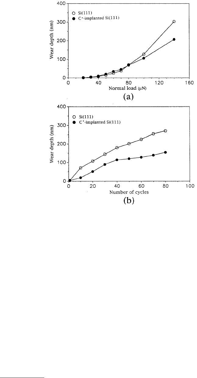
The wear resistance of ion-implanted silicon samples was further studied, Figure 16.11 (Bhushan and
Koinkar, 1994). For tests conducted at various loads on Si(111) and C
+
-implanted Si(111), it is noted
that wear resistance of implanted sample is slightly poorer than that of virgin silicon up to about 80 µN.
Above 80 µN, the wear resistance of implanted Si improves. As one continues to run tests at 40 µN for
a larger number of cycles, the implanted sample exhibits higher wear resistance than the unimplanted
sample. Damage from the implantation in the top layer results in poorer wear resistance; however, the
implanted zone at the subsurface is more wear resistant than the virgin silicon.
Nanoindentation hardness values of all samples are presented in Table 16.2. Coatings and treatments
improved nanohardness of silicon. Note that dry-oxidized and PECVD films are harder than wet-oxidized
films, as these films may be porous. High hardness of oxidized films may be responsible for measured
low wear on the microscale and macroscale (data to be presented later). Figure 16.12 shows the inden-
tation marks generated on virgin and C
+
-implanted Si(111) at a normal load of 70 µN with a depth of
indentation about 3 nm and hardness values of 15.8 and 19.5 GPa, respectively (Bhushan and Koinkar,
1994). Hardness values of virgin and C
+
-implanted Si(111) at various indentation depths (normal loads)
are presented in Figure 16.13 (Bhushan and Koinkar, 1994). Note that the hardness at a small indentation
depth of 2.5 nm is 16.6 GPa and it drops to a value of 11.7 GPa at a depth of 7 nm and a normal load
of 100 µN. Higher hardness values obtained in low-load indentation may arise from the observed pres-
sure-induced phase transformation during the nanoindentation (Pharr, 1991; Callahan and Morris,
1992). Additional increase in the hardness at an even lower indentation depth of 2.5 nm reported here
may arise from the contribution by complex chemical films (not from native oxide films) present on the
silicon surface. At small volumes there is a high probability that indentation would be made into a region
that was initially dislocation free. Furthermore, at small volumes, it is believed that there is an increase
in the stress necessary to operate dislocation sources (Gane and Cox, 1970; Sargent, 1986). These are
some of the plausible explanations for an increase in hardness at smaller volumes. If the silicon material
is to be used at very light loads such as in microsystems, the high hardness of surface films would protect
the surface until it is worn.
From Figure 16.13, hardness values of C
+
-implanted Si(111) at a normal load of 50 µN is 20.0 GPa
with an indentation depth of about 2 nm which is comparable to the hardness value of 19.5 GPa at 70 µN,
whereas measured hardness value for virgin silicon at an indentation depth of about 7 nm (normal load
of 100 µN) is only about 11.7 GPa. Thus, ion implantation results in an increase in hardness. Note that
the surface layer of the implanted zone is much harder compared with the subsurface, and may be brittle
leading to higher wear on the surface. The subsurface of the implanted zone is harder than the virgin
silicon, resulting in higher wear resistance, which will be shown later in macroscale tests conducted at
high loads.
FIGURE 16.10
Scratch depth as a function of normal force after 10 cycles for various silicon samples, virgin, treated,
and coated. (From Bhushan, B. and Koinkar, V.N., 1994,
J. Appl. Phys.
75, 5741–5746. With permission.)
© 1999 by CRC Press LLC
16.3.2 Micro/Nanotribological Studies of Doped and Undoped
Polysilicon Films, SiC Films, and Their Comparison
to Single-Crystal Silicon
16.3.2.1 Surface Roughness and Friction
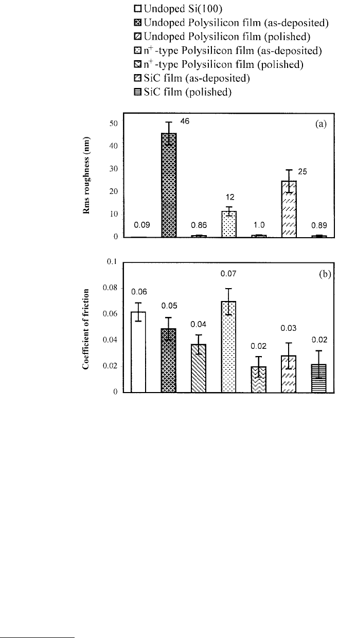
The surface roughness of various samples obtained with the AFM is compared in Figure 16.14a
(Sundararajan and Bhushan, 1998). Polishing of the as-deposited polysilicon and SiC films drastically
affect the roughness as the values reduce by two orders of magnitude. Si(100) appears to be the smoothest
followed by polished undoped polysilicon and SiC films, which have comparable roughness. The doped
polysilicon film shows higher roughness than the undoped sample, which is attributed to the doping
process. The coefficients of microscale friction of the various samples are shown in Figure 16.14b (Bhus-
han et al., 1998; Sundararajan and Bhushan, 1998). Despite being the smoothest sample, Si(100) shows
higher friction than the other samples. Doped polysilicon also shows high friction, which is due to the
presence of grain boundaries and high surface roughness. In the case of the undoped polysilicon and
SiC films, polishing did not affect the friction values by much. From the data, the polished SiC film
shows the lowest friction followed by polished, undoped polysilicon film, which strongly supports the
candidacy of SiC films for use in MEMS devices. Gray-scale top-view images of surface height and
FIGURE 16.11
Wear depth as a function of (a) load (after one cycle), and (b) cycles (normal load = 40 µN) for
Si(111) and C
+
-implanted Si(111). (From Bhushan, B. and Koinkar, V.N., 1994,
J. Appl. Phys.
75, 5741–5746. With
permission.)

© 1999 by CRC Press LLC
corresponding friction force of selected samples obtained with the AFM/FFM are shown in Figure 16.15.
Brighter regions indicate higher height than darker regions in the case of the surface height images, while
brighter regions indicate higher friction force experienced by the tip than the darker regions. The doped
polysilicon film shows a large number of grain boundaries. It appears that regions of high and low surface
height do not necessarily correspond to regions of high and low friction.
The low microscale friction exhibited by SiC compared to the other materials agrees with the fact that
many ceramic–ceramic interfaces generally show low friction on the macroscale. In this study, the Si
3
N
4
tip–SiC film interface also shows the same trend. In the case of ceramic materials, formation of tribo-
chemical films on the surface due to sliding results in low values of friction. SiC can react with water
vapor to form silicon hydroxide and oxide, which improve the frictional behavior (Xu and Bhushan,
1997). From this discussion, it can be seen that an obvious drawback with SiC is its readiness to form
tribochemical films, which is environment dependent. Another factor that affects friction in ceramic
materials is fracture, which leads to high friction because of the plowing contribution. But in the case
of SiC film, fracture toughness is believed to follow the same trend as that of the bulk material, which
is higher than that of silicon (see Table 16.1), thereby resulting in lower plowing contribution and hence
lower friction. Macroscale friction measurements indicate that SiC film exhibits one of the lowest friction
values as compared to the other samples. Doped polysilicon sample shows low friction on the macroscale
as compared to the undoped polysilicon sample possibly due to the doping effect.
16.3.2.2 Scratch/Wear Tests
As explained earlier, the scratch tests consisted of making scratches for ten cycles with varying loads.
Figure 16.16a shows a plot of scratch depth vs. normal load for various samples (Bhushan et al., 1998;
Sundararajan and Bhushan, 1998). Error bars are given for the Si(100) data. The variation was typically
about 12%. Scratch depth increases with increasing normal load. Si(100) and the doped and undoped
polysilicon film show similar scratch resistance. From the data, it is clear that the SiC film is much more
scratch resistant than the other samples. The increase in scratch depth with normal load is very small
and all depths are less than 30 nm, while the Si(100) and polysilicon films reach depths in excess of
150 nm. Figure 16.17 shows 3D images of the scratch marks.
Wear tests were conducted on the samples for one cycle at normal loads ranging from 20 to 80 µN.
The resulting wear depths are plotted against the normal loads in Figure 16.16b (Bhushan et al., 1998;
Sundararajan and Bhushan, 1998). Again, the wear depth increases with increasing normal load. Similar
to the scratch resistance data, Si(100) and the polysilicon samples also behave similarly in terms of wear
resistance. The SiC film starts out showing comparable wear depth at 20 µN to all the other samples, but
at higher loads SiC film shows superior wear resistance. Also there is hardly an increase in wear depth
with increasing normal load in the case of SiC film. The evolution of wear on the various samples was
also studied. This test was performed by wearing the same region for 20 cycles at a normal load of 20 µN,
while observing wear depths at different intervals (1, 2, 10, 15, and 20 cycles), Figure 16.18. This would
give information as to the progression of wear of the material. The wear depths observed are plotted
against the number of cycles in Figure 16.16b. For all the materials, the wear depth increases almost
linearly with increasing number of cycles. This suggests that the material is removed layer by layer in all
the materials. Here also, SiC film exhibits lower wear depths than the other samples. Doped polysilicon
film wears less than the undoped film. Not many debris particles are seen in the figures. This is due to
the fact that the debris particles created are loose and are pushed outside the imaging area by the sliding
tip during scanning. It can also be seen from the figure that the wear marks are uniform at the bottom,
indicating that uniform wear has occurred with particle pile up on the edges of the wear mark.
The wear tests clearly show that SiC film possesses an extremely wear-resistant surface compared to
the other samples and, together with the scratch tests results, indicate that SiC film has better surface
mechanical properties than Si(100) and the polysilicon films. Table 16.4 shows a summary of the various
properties of the samples measured in this study (Bhushan et al., 1998; Sundararajan and Bhushan 1998).
The superior scratch/wear resistance of the SiC film is consistent with the hardness values near the surface
measured with the nanoindenter. Higher hardness of SiC film is one of the factors responsible for its
© 1999 by CRC Press LLC
better scratch/wear resistance. Wear in ceramic materials in the case of asperity contacts occurs due to
brittle fracture. As the AFM tip slides over the material surface, Hertzian cone cracks can occur when
the normal stress exceeds a critical value (Hutchings, 1992). Friction (tangential) forces during sliding
reduce this critical value. High fracture toughness and low coefficient of friction of SiC film help in
reducing the chances of brittle fracture, which results in low wear. Therefore, abrasive wear due to plastic
deformation and fracture govern the wear process. In the case of all samples, surface reactions result in
the formation of tribochemical films that are different in nature than the underlying material. Therefore,
at low loads and at the onset of wear, all samples would show similar wear depths as they all have
comparable interfacial shear strengths and attack angles (attack angle is the included angle between the
leading face of the asperity and the contact plane at the point of contact). This is seen in the case of the
reported wear depths at 20 µN for 1 cycle (Figure 16.16b). In the case of the scratch test data
(Figure 16.16a), SiC shows slightly lower scratch depth at 20 µN since the data is for ten cycles, during
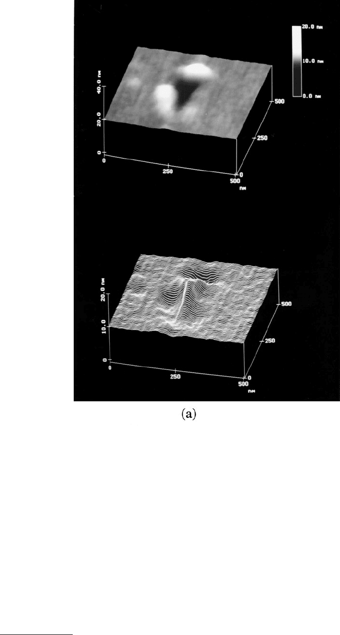
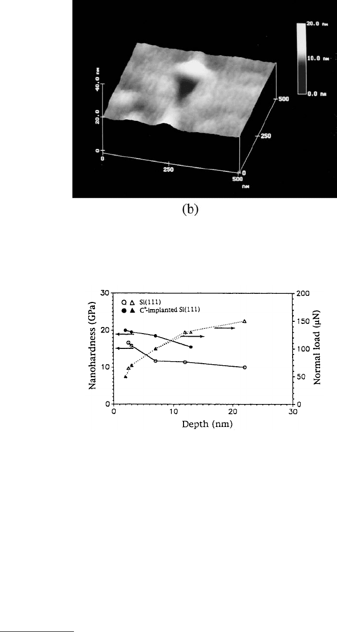
FIGURE 16.12
© 1999 by CRC Press LLC
which time it is possible that the bulk properties of the material start coming into play in addition to
that of the tribochemical films. This is consistent with the wear depths at 20 µN for ten cycles and more
(Figure 16.16c). As the normal load increases, Si(100) and polysilicon films show a sharp increase in
degree of penetration (ratio of groove depth to radius of contact) and attack angle, which leads to higher
wear (Hokkirigawa and Kato, 1988; Koinkar and Bhushan, 1997). Higher fracture toughness and higher
hardness of SiC as compared to Si(100) is responsible for its lower wear. Also the higher thermal
conductivity of SiC (see Table 16.1) as compared to the other materials leads to lower interface temper-
atures which generally results in less degradation of the surface (Bhushan, 1996a). Doping of the poly-
silicon does not affect the scratch/wear resistance and hardness much. The measurements made on the
doped sample are affected by the presence of grain boundaries.
FIGURE 16.12
Gray-scale plot and line plot of the inverted nanoindentation mark on (a) Si(111) at 70 µN (hardness
~ 15.8 GPa), and (b) gray-scale plot of indentation mark on C
+
-implanted Si(111) at 70 µN (hardness ~ 19.5 GPa).
The indentation depth of indent was about 3 nm.
FIGURE 16.13
Nanohardness and normal load as function of indentation depth for virgin and C
+
-implanted
Si(111). (From Bhushan, B. and Koinkar, V.N., 1994,
J. Appl. Phys.
75, 5741–5746. With permission.)
© 1999 by CRC Press LLC
16.3.2.3 Hardness, Elastic Modulus, and Fracture Toughness Measurements
Representative load–displacement curves of indentations made at 0.2 and 15 mN peak indentation loads
on various samples are shown in Figure 16.19. Measured hardness, elastic modulus, and fracture tough-
ness values are given in Table 16.4 (Bhushan et al., 1998; Li and Bhushan, 1998; Sundararajan and
Bhushan, 1998). Properties of undoped polysilicon films are comparable to that of bulk single-crystal
silicon. Doping of the polysilicon film degrades its mechanical properties. SiC film shows hardness and
elastic modulus higher than the other samples. Higher hardness of SiC is believed to be responsible for
its superior scratch/wear resistance compared to the other samples.
16.3.3 Macroscale Tribological Studies of Virgin, Coated,
and Treated Samples
To study the effect of ion implantation of silicon on friction and wear, single-crystalline and polycrystalline
silicon samples were ion implanted by Gupta et al. (1993, 1994) and Gupta and Bhushan (1994) with
FIGURE 16.14
Comparisons of (a) rms surface roughness and (b) coefficient of microscale friction values for
various samples. (From Bhushan, B. et al., 1998, in
Tribology Issues and Opportunities in MEMS,
B. Bhushan, ed.,
Kluwer Academic, Dordrecht. With permission.)