Cao Z. (Ed.) Thin Film Growth: Physics, materials science and applications
Подождите немного. Документ загружается.

208 Thin film growth
© Woodhead Publishing Limited, 2011
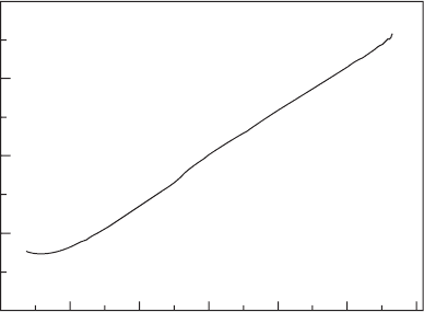
can be an exponential-like function of 1/T. With decreasing temperature,
the number of carriers decreases while the mobility generally increases,
but in different manners; consequently, the resulting electrical resistivity is
exclusively temperature dependent. For narrow band-gap semiconductors
and semimetals, the situation is more complicated than in the conventional
semiconductors like Si or Ge. The carrier distribution function obeys the
Fermi–Dirac statistics which in this case cannot be approximated by the
Maxwell–Boltzmann formula. Moreover, the conduction band is Kane-type
that the effective mass of electron, thus the mobility of electron, changes
with the carrier density (Lovett 1977). The vanishing TCR occurs when
this compound has narrowed its band-gap to be a semimetal for which the
temperature dependence of the number of the carriers becomes rather mild-
mannered in contrast to the situation in a semiconductor of a denite band-
gap. It results from a delicate balance between the opposite changes of the
number of carriers and of the carrier mobility with temperature, and reasonably
it appears only at temperatures below 240 K – at higher temperatures the
increasing number of carriers can easily compensate for the loss in carrier
mobility to give rise to a rapidly decreasing electrical resistivity. The current
discovery, though lacking a clear scenario of detailed microscopic processes
due to the difculty in calculating the band structure for the off-stoichiometric
compounds such as Cu
3
NPd
0.238
and in performing Hall measurement for some
supplementary information, does demonstrate the possibility that a balanced
change of carrier density and carrier mobility over a wide temperature range
is in principle possible in a class of semimetallic materials. Considering the
unlikelihood of a temperature-independent electrical resistivity for solids,
the current result also bears some signicance for solid state physics.
Resistivity (10
–6
Wm)
1.4
1.3
1.2
1.1
1.0
0 50 100 150 200 250 300
Temperature (K)
(f)
8.15 Continued.
ThinFilm-Zexian-08.indd 208 7/1/11 9:42:10 AM
209Thin film growth for thermally unstable noble-metal nitrides
© Woodhead Publishing Limited, 2011
8.5 Conclusions
By carefully adjusting the working parameters including the applied power, gas
pressure and the ratio of nitrogen in the working gas, and substrate temperature,
thin lms of noble-metal nitrides such as Cu
3
N and Cu
3
NPd
x
can be successfully
prepared by using the reactive magnetron sputtering method. For stoichiometric
Cu
3
N, the lms are found to comprise distinct crystallites in a typical size
of 40–60 nm. The peculiarity of growing noble-metal nitride lms lies in the
fact that the reaction of sputtered metal atoms or clusters with nitrogen occurs
most probably only at the target surface, hence the matching of the density and
energy of nitrogen ions with the sputtering yield for a chosen target material is
the key factor to realizing stoichiometry in the resulting copper nitride lms. A
large ion energy is unfavorable since the higher sputtering yield of the metal
atoms and the weakened combination with energetic nitrogen ions will give
rise to a metal-rich deposit. A low substrate temperature is critical since at
slightly elevated temperatures nitrogen re-emission occurs, which may even
result in microsized protruding features. Semiconducting to (semi)metallic
transition can be observed in doped Cu
3
N structures wherein the excessive
atoms are expected to sit at the cell centers of the Cu
3
N lattice. A vanishing
temperature coefcient of resistivity over a temperature of 200 K has been
realized in Cu
3
NPd
0.238
. Many other surprising properties are anticipated in
the noble-metal nitrides, which await discovery in the future.
8.6 References
Asano M, Umeda K, and Tasaki A (1990), Cu
3
N thin lm for a new light recording
media, Jpn. J. Appl. Phys. 29, 1985–1986.
Baranov O, Romanov M, Wolter M, Kumar S, Zhong X X, and Ostrikov K (2010),
Low-pressure planar magnetron discharge for surface deposition and nanofabrication,
Physics of Plasma 17, 053509.
Berg S, and Nyberg T (2005), Fundamental understanding and modeling of reactive
sputtering processes, Thin Solid Films 476, 215–230.
Borsa D M, Grachev S, Presura C, and Boerma D O (2002), Growth and properties of
Cu
3
N lms and Cu
3
N/g-Fe
4
N bilayers, Appl. Phys. Lett. 80, 1823–1825.
Cao Z X (2001), Electron cyclotron waveresonance plasma assisted deposition of cubic
boron nitride thin lms, J. Vac. Sci. Technol. A 19, 485–489.
Cao Z X (2002), Plasma enhanced deposition of silicon carbonitride lms and property
characterization, Diamond & Relat. Mater. 11, 16–21.
Cao Z X, and Oechsner H (2004), Effect of concurrent N
2
+
-ion bombardment on the physical
vapor deposition of nitrides thin lms, J. Vac. Sci. Technol. A 22(2), 321–323.
Chambers S A (2010), Epitaxial growth and properties of doped transition metal and
complex oxide lms, Adv. Mater. 22(2), 219–248.
Cremer R, Witthaut M, Neuschutz D, Trappe C, Laurenzis M, Winkle O, and Kurz H
(2000), Deposition and characterization of metastable Cu
3
N layers for applications
in optical data storage, Mikro. Acta. 133, 299–302.
Dorranian D, Dejam L, Sari A H, and Hojabri A (2010), Structural and optical properties
ThinFilm-Zexian-08.indd 209 7/1/11 9:42:10 AM
210 Thin film growth
© Woodhead Publishing Limited, 2011
of copper nitride thin lms in a reactive Ar/N
2
magnetron sputtering system, Euro.
Phys. J.-Appl. Phys. 50, 20503.
Du Y, Ji A L, Ma L B, Wang Y Q, and Cao Z X (2005), Electrical conductivity and
photoreectance of nanocrystalline copper nitride thin lms deposited at low temperature,
J. Crystal Growth 280, 490–494.
Hahn U, and Weber W (1996), Electronic structure and chemical-bonding mechanism of
Cu
3
N, Cui
3
NPd, and related Cu(I) compounds, Phys. Rev. B 53, 12684–12693.
Hojabri A, Haghighian N, Yasserian K, and Ghoranneviss M (2010), The effect of nitrogen
plasma on copper thin lm deposited by DC magnetron sputtering, IOP Conf. Ser.:
Mater. Sci. Eng. 12, 012004.
Jacobs H, and Zachwieja U (1991), Kupferpalladiumnitride, Cu
3
Pd
x
N mit x = 0.020
und 0.989, Perowskite mit ‘bindender 3d
10
-4d
10
-Wechselwirkung’, J. Less-common
Met. 170, 185–190.
Ji A L, Li C R, Du Y, Ma L B, Song R, and Cao Z X (2005), Formation of rosette pattern
in copper nitride thin lms via nanocrystals gliding, Nanotech. 16, 2092–2095.
Ji A L, Huang R, Du Y, Li C R, and Cao Z X (2006a), Growth of stoichiometric Cu
3
N
thin lms by reactive magnetron sputtering, J. Crystal. Growth 295, 79–83.
Ji A L, Li C R, and Cao Z X (2006b), Ternary Cu
3
NPd
x
exhibiting invariant electrical
resisitivity over 200 K, Appl. Phys. Lett. 89, 252120.
Ji A L, Du Y, Li C R, and Cao Z X (2007), Formation of symmetrical relief features in
nanocrystalline copper nitride thin lms, J. Vac. Sci. Technol. B 25 (1), 208–211.
Juza R, and Hahn H (1939), Copper nitride (in German), Z. Anorg. Allg. Chem. 241,
172–178.
Kim K J, Kim J H, and Kang J H (2001), Structural and optical characterization of
Cu
3
N lms prepared by reactive RF magnetron sputtering, J. Crystal Growth 222,
767–772.
Lovett D R (1977), Semimetals & Narrow-bandgap Semiconductors, Pion Limited,
London.
Ma G M, Alejandro M, and Noboru T (2004), Ab initio total energy calculations of copper
nitride: the effect of lattice parameters and Cu content in the electronic properties,
Solid Stat. Sci. 6, 9–14.
Maruyama T, and Morishita T (1996), Copper nitride and tin nitride thin lms for write-
once optical recording media, Appl. Phys. Lett. 69, 890–891.
Moreno-Armenta M G, Martínez-Ruiz A, and Takeuchi N (2004), Ab initio total energy
calculations of copper nitride: the effect of lattice parameters and Cu content in the
electronic properties, Solid State Sciences 6, 9–14.
Musil J, Baroch P, Vlcek J, Nam K H, and Han J G (2005), Reactive magnetron sputtering
of thin lms: present status and trends, Thin Solid Films 475, 208–218.
Norskov J K, and Hammer B (1995), Why gold is the noblest of all the metals, Nature
376, 238–240.
Nosaka T, Yoshitake M, Okamoto A, Ogawa S, and Nakayama Y (2001), Thermal
decomposition of copper nitride thin lms and dots formation by electron beam
writing, Appl. Surf. Sci. 169–170, 358–361.
Reddy K V S, Reddy A S, Reddy P S, and Uthanna S (2007), Copper nitride lms
deposited by dc reactive magnetron sputtering, J. Mater. Sci. – Materials in Electronics
18, 1003–1008.
Terada S, Tanaka H, and Kubota K (1989), Heteroepitaxial growth of Cu
3
N thin lms,
J. Crystal Growth 94, 567–568.
Wang D Y, Nakamine N, and Hayashi Y (1998), Properties of various sputter-deposited
Cu–N thin lms, J. Vac. Sci. Technol. A 16, 2084–2092.
ThinFilm-Zexian-08.indd 210 7/1/11 9:42:10 AM

© Woodhead Publishing Limited, 2011
211
9
Growth of graphene layers for thin films
B. H. Hong and H. R. Jeon, Sungkyunkwan University,
South Korea
Abstract: graphene has received considerable attention due to its fascinating
physical properties such as quantum electronic transport, a tunable band gap,
extremely high mobility, high elasticity and electromechanical modulation.
This chapter describes the direct synthesis of large-scale graphene lms
using chemical vapour deposition on thin nickel layers, and presents two
different methods of patterning the lms and transferring them to arbitrary
substrates. Furthermore, we detail the roll-to-roll production and wet
chemical doping of predominantly monolayer 30-inch graphene lms grown
by chemical vapour deposition onto exible copper substrates.
Key words: graphene growth, chemical vapour deposition, half-integer
quantum Hall effect, roll-to-roll production.
9.1 Introduction
In order to be used as nano-electronic devices, it is essential to grow graphene
on a large scale. Among methods for graphene synthesis, graphene growth
by chemical vapour deposition (CVD) on ni and Cu has the advantage of
growing graphene at large scale with uniform thickness. This chapter deals
with graphene growth on ni and Cu by CVD. First we describe large-scale
graphene lm synthesis using CVD on nickel layers, their pattern and their
transfer to arbitrary substrates.
1
In next section we detail the roll-to-roll
production and wet chemical doping of predominantly monolayer 30-inch
graphene lms grown by CVD onto exible copper substrates.
2
Further, we
detail how graphene electrodes were incorporated into a fully functional
touchscreen panel device capable of withstanding high strain.
9.2 Large-scale pattern growth of graphene films
for stretchable transparent electrodes
9.2.1 Direct synthesis of large-scale graphene films
Ni lms were e-beam evaporated on SiO
2
/Si substrates, and thermally
annealed. After exposing the ni surface to a CH
4
, H
2
and Ar mixture in
atmospheric conditions, the system was rapidly cooled to room temperature.
This fast cooling rate is critical in suppressing formation of multiple layers
ThinFilm-Zexian-09.indd 211 7/1/11 9:42:28 AM
212 Thin film growth
© Woodhead Publishing Limited, 2011
and for separating graphene layers efciently from the substrate in the later
process.
3
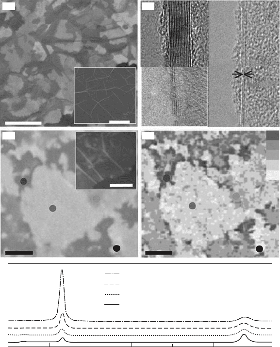
A scanning electron microscope (SEM) image of graphene lms on a thin
nickel substrate shows clear contrast between areas with different numbers
of graphene layers (Fig. 9.1a). Transmission electron microscope (TeM)
images (Fig. 9.1b) show that the lm consists mostly of less than a few layers
of graphene. After transfer of the lm to a silicon substrate with a 300 nm
thick Sio
2
layer, optical and confocal scanning Raman microscope images
were made of the same area (Fig. 9.1c,d).
4
The brightest area in Fig. 9.2(d)
corresponds to monolayers, and the darkest area is composed of more than
ten layers of graphene. Bilayer structures appear to predominate in both
TeM and Raman images for this particular sample, which was prepared
from 7 minutes of growth on a 300 nm thick nickel layer. It is found that
the average number of graphene layers, the domain size and the substrate
coverage can be controlled by changing the nickel thickness and growth
process, thus providing a way of controlling the growth of graphene for
different applications.
Atomic force microscope (AFM) images often show the ripple structures
caused by the difference between the thermal expansion coefcients of nickel
and graphene (Fig. 9.1c).
5
It is believed that these ripples make the graphene
lms more stable against mechanical stretching,
6
making the lms more
expandable. Multilayer graphene lms are preferable in terms of mechanical
strength for supporting large-area lm structures, whereas thinner graphene
lms have higher optical transparency. It is found that a ~300 nm thick
nickel layer on a silicon wafer is the optimal substrate for the large-scale
CVD growth that yields mechanically stable, transparent graphene lms to
be transferred and stretched after they are formed, and that thinner nickel
layers with a shorter growth time yield predominantly mono- and bilayer
graphene lm for microelectronic device application.
9.2.2 Transfer processes for large-scale graphene films
The transfer of CVD-derived graphene lms to non-specic substrates is
enabled by FeCl
3
etching of the underlying Ni lm. Use of buffered oxide
etchant (BOE) or hydrogen uoride solution removes silicon dioxide layers,
so the patterned graphene and the nickel layer oat together on the solution
surface. After transfer to a substrate, further reaction with Boe or hydrogen
uoride solution completely removes the remaining nickel layers.
A dry-transfer process has been developed for the graphene lm using
a soft substrate such as polydimethylsiloxane (PDMS) stamp.
7
Here the
PDMS stamp is rst attached to the CVD-grown graphene lm on the
nickel substrate (Fig. 9.2d). The nickel substrate can be etched away using
FeCl
3
as described above, leaving the adhered graphene lm on the PDMS
ThinFilm-Zexian-09.indd 212 7/1/11 9:42:28 AM
213Growth of graphene layers for thin films
© Woodhead Publishing Limited, 2011
(a)
(c)
(b)
(d)
5 µm
5 µm
2 µm
2 µm
5 µm
4–5 layers Bilayer
0.34 nm
>10 layers
3 layers
>5
4
3
2
1
Intensity (a.u.)
D
G
2D
l = 532 nm
>4 layers
3 layers
Bilayer
Monolayer
1500 2000 2500
Raman shift (cm
–1
)
(e)
9.1 Various spectroscopic analyses of large-scale graphene films
grown by CVD. (a) SEM images of as-grown graphene films on
thin (300 nm) nickel layers and thick (1 mm) Ni foils (inset). (b)
TEM images of graphene films of different thickness. (c) An optical
microscope image of the graphene films transferred to a 300 nm
thick silicon dioxide layer. The inset AFM image shows typical rippled
structures. (d) A confocal scanning Raman image corresponding to
(c). The number of layers is estimated from the intensities, shapes
and positions of the G-band and 2D-band peaks. (e) Raman spectra
(532 nm laser wavelength) obtained from the corresponding coloured
spots in (c) and (d). a.u. = arbitrary units. (From Ref. [1].)
ThinFilm-Zexian-09.indd 213 7/1/11 9:42:28 AM
214 Thin film growth
© Woodhead Publishing Limited, 2011
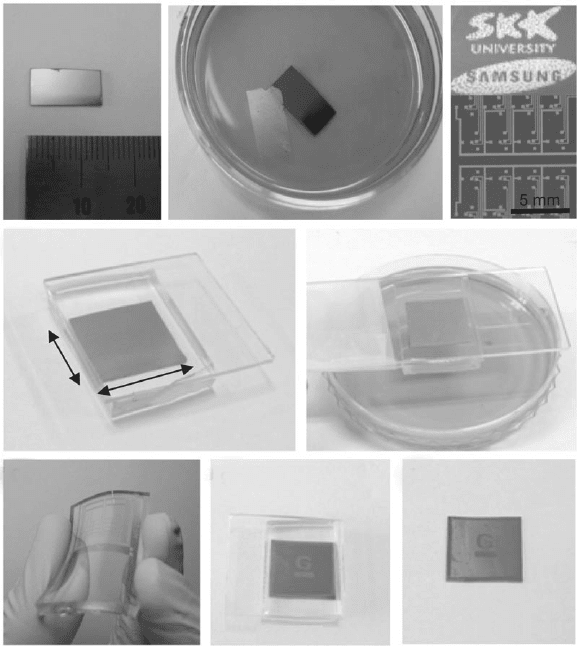
substrate (Fig. 9.2e). By using the pre-patterned nickel substrate (Fig. 9.2c),
we can transfer various sizes and shapes of graphene lm to an arbitrary
substrate. This dry-transfer process turns out to be very useful in making
large-scale graphene electrodes and devices without additional lithography
(a) (b) (c)
(e)
(d)
(f) (g)
(h)
2 cm
2 cm
Stamping Patterned graphene
9.2 Transfer processes for large-scale graphene films. (a) A
centimeter-scale graphene film grown on Ni(300 nm)/SiO
2
(300 nm)/Si
substrate. (b) A floating graphene film after etching the nickel layers
in 1M FeCl
3
aqueous solution. After the removal of the nickel layers,
the floating graphene film can be transferred by direct contact with
substrates. (c) Various shapes of graphene films can be synthesized
on top of patterned nickel layers. (d, e) The dry-transfer method
based on a PDMS stamp is useful in transferring the patterned
graphene films. After attaching the PDMS substrate to the graphene
(d), the underlying nickel layer is etched and removed using
FeCl
3
solution (e). (f) Graphene films on the PDMS substrates are
transparent and flexible. (g, h) The PDMS stamp makes conformal
contact with a silicon dioxide substrate. Peeling back the stamp (g)
leaves the film on a SiO
2
substrate (h). (From Ref. [1].).
ThinFilm-Zexian-09.indd 214 7/1/11 9:42:29 AM
215Growth of graphene layers for thin films
© Woodhead Publishing Limited, 2011
processes (Fig. 9.2f–h). Microscopically, these graphene lms often show
linear crack patterns with an angle of 60°C or 120°C, indicating a particular
crystallographic edge with large crystalline domains. In addition, the Raman
spectra measured for graphene lms on nickel substrates show a strongly
suppressed defect-related D-band peak. This D peak grows only slightly
after the transfer process (Fig. 9.1e), indicating overall good quality of the
resulting graphene lm. Further optimization of the transfer process with
substrate control makes possible transfer yields approaching 99%.
9.2.3 Optical and electrical properties of the graphene
films
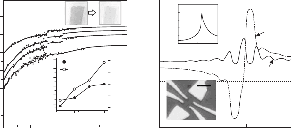
For the macroscopic transport electrode application, the optical and electrical
properties of 1 ¥ 1 cm
2
graphene lms were measured by ultraviolet-visible
spectrometer and four-probe Van der Pauw methods, respectively (Fig. 9.3a,b).
The transmittance is measured using an ultraviolet-visible spectrometer after
transferring the oating graphene lm to a quartz plate (Fig. 9.3a). In the
visible range, the transmittance of the lm grown on a 300 nm thick nickel
layer for 7 minutes is ~80%, a value similar to those found for previously
studied assembled lms.
8,9
Because the transmittance of the graphene layer
is ~2.3%,
10
this transmittance can be increased to ~93% by further reducing
the growth time and nickel thickness, resulting in a thinner graphene lm.
Ultraviolet/ozone etching is also useful in controlling the transmittance under
ambient conditions (Fig. 9.4a, upper inset). Indium electrodes were deposited
on each corner of the square (Fig. 9.3a, lower inset) to minimize contact
resistance. The minimum sheet resistance is ~280W per square, which is
~30 times smaller than the lowest sheet resistance measured on assembled
lms.
8,9
The values of sheet resistance increase with the ultraviolet/ozone
treatment time, in accordance with the decreasing number of graphene layers
(Fig. 9.3a)
For microelectronic application, the mobility of the graphene lm is
critical. To measure the intrinsic mobility of a single-domain graphene
sample, the graphene samples are transferred from a PDMS stamp to a
degenerate doped silicon wafer with a 300 nm deep thermally grown oxide
layer. Monolayer graphene samples were readily located on the substrate
from optical contrast
10
and their identication was subsequently conrmed
by Raman spectroscopy.
4
electron beam lithography was used to make
multi-terminal devices (Fig. 9.3b, lower inset). notably, the multi-terminal
electrical measurements showed that the electron mobility is ~3750 cm
2
V
–1
s
–1
at a carrier density of ~5 ¥ 10
12
cm
–2
(Fig. 9.3b). For a high magnetic
eld of 8.8T, the half-integer quantum Hall effect (Fig. 9.3b) is observed,
indicating that the quality of CVD-grown graphene is comparable to that of
mechanically cleaved graphene.
ThinFilm-Zexian-09.indd 215 7/1/11 9:42:29 AM
216 Thin film growth
© Woodhead Publishing Limited, 2011
Transmittance (%)
90
85
80
75
70
65
60
83.7% UV for 6 h
80.7% UV for 4 h
79.1% UV for 2 h
76.3% Initial
at 550 nm
LIV
R
s
(kW per
square)
1.2
1.0
0.8
0.6
0.4
0.2
84
82
80
78
76
0 1 2 3 4 5 6
Time (h)
Tr (%)
400 600 800 1000 1200
Wavelength (nm)
(a)
–60 –40 –20 0 20 40 60
V
g
(V)
(b)
5 µm
Magnetoresistance (kW)
Resistance (kW)
10
5
0
–5
–10
–15
4
2
0
–60 0 60
V
g
(V)
R
xy
R
xx
9.3 Optical and electrical properties of graphene films. (a)
Transmittance of the graphene films on a quartz plate. The
discontinuities in the absorption curves arise from the different
sensitivities of the switching detectors. The upper inset shows the
ultraviolet (UV)-induced thinning and the consequent enhancement
of transparency. The lower inset shows the changes in transmittance,
T
r
, and sheet resistance, R
s
, as functions of ultraviolet illumination
time. (b) Electrical properties of monolayer graphene devices
showing half-integer quantum Hall effect and high electron
mobility. The upper inset shows a four-probe electrical resistance
measurement on a monolayer graphene Hall bar device (lower inset)
at 1.6 K. A gate voltage, V
g
, is applied to the silicon substrate to
control the charge density in the graphene sample. The main panel
shows longitudinal (R
xx
) and transverse (R
xy
) magnetoresistances
measured in this device for a magnetic field B = 8.8T. The monolayer
graphene quantum Hall effect is clearly observed, showing the
plateaux with filling factor u = 2 at R
xy
= (2e
2
/h)
–1
and zeros in
R
xx
. (Here e is the elementary charge and h is Plank’s constant.)
Quantum Hall plateaux (horizontal dashed lines) are developing for
higher filling factors. (c) Variation in resistance of a graphene film
transferred to a ~0.3 mm thick PDMS/PET substrate for different
distances between holding stages (that is, for different radii). The
left inset shows the anisotropy in four-probe resistance, measured
as the ratio R
y
/R
x
, of the resistances parallel and perpendicular to
the binding direction, y. The right inset shows the bending process.
(d) Resistance of a graphene film transferred to a PDMS substrate
isotropically stretched by ~12%. The left inset shows the case in
which the graphene film is transferred to an unstretched PDMS
substrate. The right inset shows the movement of holding stages
and the consequent change in shape of the graphene film. (From Ref.
[1].)
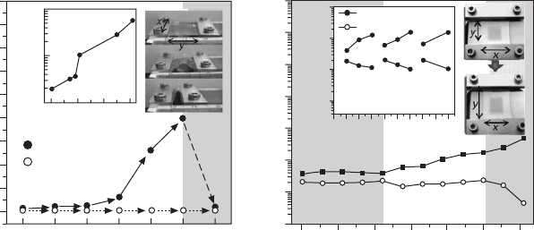
In addition to the good optical and electrical properties, the graphene lm
has excellent mechanical properties when used to make exible and stretchable
electrodes (Fig. 9.3c,d).
7
The foldability of the graphene lms, transferred
ThinFilm-Zexian-09.indd 216 7/1/11 9:42:29 AM
217Growth of graphene layers for thin films
© Woodhead Publishing Limited, 2011
to a polyethylene terephthalate (PET) substrate (thickness, ~100 mm) coated
with a thin PDMS layer (thickness, ~200 mm; Fig. 9.3c), is evaluated by
measuring resistances with respect to bending radii. The resistances show
little variation up to the bending radius 2.3 mm (approximate tensile strain
of 6.5%), and are perfectly recovered after unbending. notably, the original
resistance can be restored even for the bending radius of 0.8 mm (approximate
tensile strain of 18.7%), exhibiting extreme mechanical stability in comparison
with conventional materials used in exible electronics.
11
The resistance of graphene lms transferred to pre-strained and unstrained
PDMS substrates was measured with respect to uniaxial tensile strain ranging
from 0 to 30% (Fig. 9.3d). Similar to the results in the folding experiment,
the transferred lm on the unstrained substrate recovers its original resistance
after stretching by ~6% (Fig. 9.3d, left inset). However, further stretching
often results in mechanical failure. Thus, it was tried transferring the lm
to pre-strained substrates
12
to enhance the electromechanical stabilities by
creating ripples similar to those observed in the growth process (Fig 9.1c,
inset). The graphene transferred to a longitudinally strained PDMS substrate
does not show much enhancement, owing to the transverse strain induced
by Poisson’s effect.
13
To prevent this problem, the PDMS substrate was
isotopically stretched by ~12% before transferring the lm to it (Fig. 9.3d).
Surprisingly, both longitudinal and transverse resistance (R
y
and R
x
) appear
stable up to ~11% stretching and show only one order of magnitude change
at ~25% stretching. It is supposed that further uniaxial stretching can change
the electronic band structure of graphene, leading to the modulation of sheet
resistance. These electrochemical properties thus show graphene lms to be
not only the strongest
14
but also the most exible and stretchable conducting
transparent materials so far measured.
10
Resistance (W)
10
4
10
3
10
2
10
1
R
y
R
y
R
x
R
x
1st 2nd 3rd
Stretching cycles
0 3 6 0 3 6 0 3 6
Stretching (%)
Stable
Resistance (W)
Resistance (kW)
10
8
10
7
10
6
10
5
10
4
10
3
10
2
10
1
9
8
7
6
5
4
3
2
1
0
0 5 10 15 20 25 30
Stretching (%)
(d)
Flat 3.5 2.7 2.3 1.0 0.8 Flat
Bending radius (mm)
(c)
Anisotropy, R
y
/R
x
10
2
10
1
10
0
R
y
R
x
0.0 0.4 0.8 1.2
Curvature, k
(mm
–1
)
Bending Recovery
9.3 Continued
ThinFilm-Zexian-09.indd 217 7/1/11 9:42:29 AM