Cao Z. (Ed.) Thin Film Growth: Physics, materials science and applications
Подождите немного. Документ загружается.

218 Thin film growth
© Woodhead Publishing Limited, 2011
9.3 Roll-to-roll production of 30-inch graphene
films for transparent electrodes
9.3.1 Synthesis of 30-inch graphene films and roll-to-roll
transfer of graphene films
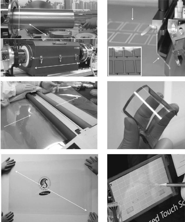
Figures 9.4a–c present photographs of the roll-based synthesis and transfer
process. An 8-inch-wide tubular quartz reactor (Fig. 9.4a) is used in the
CVD system, allowing a monolayer graphene lm to be synthesized on a
roll of copper foil with dimensions as large as 30 inches in the diagonal
direction (Fig. 9.4c). A temperature gradient usually exists that depends
on the radial position inside the tubular reactor. In our preliminary work,
this sometimes resulted in inhomogeneous growth of the graphene on the
copper foils. To solve this problem, a ~7.5-inch quartz tube wrapped with
a copper foil was inserted and suspended inside the 8-inch quartz tube. In
this way, the radial inhomogeneity in the reaction temperature could be
minimized. In the rst step of synthesis, the roll of copper foil is inserted
into a tubular quartz tube and then heated to 1000°C with owing 8 standard
cubic centimetres per minute) (sccm) H
2
at 90 mtorr. After reaching 1000°C,
the sample is annealed for 30 minutes without changing the ow rate or
pressure. The copper foils are heat-treated to increase the grain size from
a few micrometers to ~100 mm, as we have found that the copper foils
with larger grain size yield higher-quality graphene lms, as suggested by
Li and colleagues.
15
The gas mixture of CH
4
and H
2
is then owed at 460
mtorr at rates of 24 and 8 sccm for 30 minutes, respectively. Finally, the
sample is rapidly cooled to room temperature (~10°C s
–1
) with owing H
2
under a pressure of 90 mtorr.
After growth, the graphene lm grown on copper foil is attached to a
thermal release tape by applying soft pressure (~0.2 MPa) between two rollers.
After etching the copper foil in a plastic bath lled with copper etchant, the
transferred graphene lm on the tape is rinsed with deionized water to remove
residual etchant, and is ready to be transferred to any kind of at or curved
surface on demand. The graphene lm on the thermal release tape is inserted
between the rollers together with a target substrate (Fig. 9.4b). By repeating
these steps on the same substrate, multilayered graphene lms can be prepared
that exhibit enhanced electrical and optical properties, as demonstrated by Li
and colleagues using wet-transfer methods at the centimeter scale.
16
Figure
9.4(c) shows the 30-inch multilayer graphene lm transferred to a roll of 188
mm thick polyethylene terephthalate (PeT) substrate. Figure 9.4(d) shows
a screen-printing process used to fabricate four-wire touchscreen panels
17
based on graphene/PET transparent conducting lms. After printing electrodes
and dot spacers, the upper and lower panels are carefully assembled and
connected to a controller installed in a laptop computer (Figs 9.4e and f),
ThinFilm-Zexian-09.indd 218 7/1/11 9:42:29 AM
219Growth of graphene layers for thin films
© Woodhead Publishing Limited, 2011
(a)
(b)
(c)
(d)
(e)
(f)
8 inch
39 inch
Stencil mask
Screen
printer
After
heating
Before
heating
1st
2nd
30 inch
9.4 Photographs of the roll-based production of graphene films. (a)
Copper foil wrapping around 7.5 inch quartz tube to be inserted into
an 8 inch quartz reactor. The lower image shows the stage in which
the copper foil reacts with CH
4
and H
2
gases at high temperatures.
(b) Roll-to-roll transfer of graphene films from a thermal release tape
to a PET film at 120°C. (c) A transparent ultra-large-area graphene
film transferred on a 35 inch PET sheet. (d) Screen printing process
of silver paste electrodes on graphene/PET film. The inset shows 3.1
inch graphene/PET panels patterned with silver electrodes before
assembly. (e) An assembled graphene/PET touch panel showing
outstanding flexibility. (f) A graphene-based touchscreen panel
connected to a computer with control software. (From Ref. [2].)
ThinFilm-Zexian-09.indd 219 7/1/11 9:42:29 AM
220 Thin film growth
© Woodhead Publishing Limited, 2011
which shows extraordinary exibility. The scalability and processability of
CVD graphene and the roll-to-roll methods presented here are expected to
enable the continuous production of graphene-based electronic devices at
large scales.
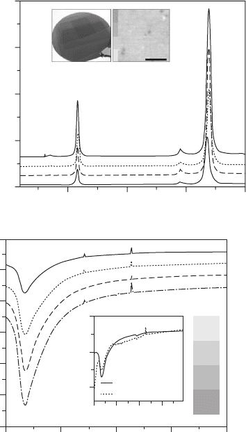
The graphene lms seem to be predominantly composed of monolayers
when analysed using Raman spectra (Fig. 9.5a). However, atomic force
microscope (AFM) and transmission electron microscope (TeM) images often
show bilayer and multilayer islands. As the graphene layers are transferred
one after another,
16
the intensities of the g- and 2D-band peaks increase
together, but their ratios do not change signicantly. This is because the
hexagonal lattices of the upper and lower layers are randomly oriented,
unlike the graphite, so the original properties of each monolayer remain
unchanged, even after stacking into multilayers;
18,19
this is clearly different
from the case of multilayer graphene exfoliated from graphite crystals.
4
The
randomly stacked layers behave independently without signicant change in
the electronic band structures, and the overall conductivity of the graphene
lms appears to be proportional to the number of stacked layers.
16
The
optical transmittance is usually reduced by ~2.2–2.3% for an additional
transfer, implying that the average thickness is approximately a monolayer
(Fig. 9.5b).
10
The unique electronic band structure of graphene allows modulation of the
charge carrier concentrations, depending on an electric eld induced by gate
bias
20
or chemical doping,
21
resulting in enhancement of sheet resistance.
We tried various types of chemical doping methods, and found that nitric
acid is very effective for p-doping of graphene lms. Figure 9.5(c) shows
Raman spectra of the graphene lms before and after doping with 63 wt%
Hno
3
for 5 minutes. The large peak shift (Du = 18 cm
–1
) indicates that the
graphene lm is strongly p-doped. The shifted g peak is often split near the
randomly stacked bilayer islands, as shown in Fig. 9.5(c). We hypothesize
that the lower graphene layer, which is screened by top layers, experiences
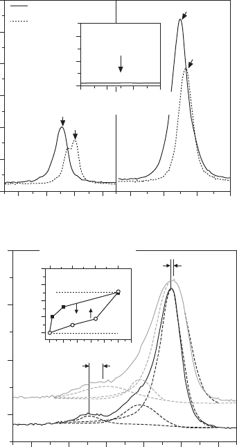
a reduced doping effect, leading to g-band splitting. In X-ray photoelectron
spectra (XPS), the C 1s peaks corresponding to sp
2
and sp
3
hybridized
states are shifted to lower energy, similar to the case for p-doped carbon
nanotubes.
21
However, multilayer stacking results in blueshifted C1s peaks.
We suppose that weak chemical bonding such as p-p stacking interaction
causes descreening of nucleus charge, leading to an overall increase in core
electron binding energies. We also nd that the work functions of graphene
lms as estimated by UV photoelectron spectroscopy (UPS) are blueshifted
by ~130 meV with increasing doping time (Fig. 9.5d, inset). The multiple
stacking also changes the work functions (Fig. 9.5d, inset) which could be
very important in controlling the efciency of photovoltaic
22
or light-emitting
devices based on graphene transparent electrodes.
23
ThinFilm-Zexian-09.indd 220 7/1/11 9:42:29 AM
221Growth of graphene layers for thin films
© Woodhead Publishing Limited, 2011
9.5 Optical characterizations of the graphene films prepared using
layer-by-layer transfer on SiO
2
/silicon and PET substrates. (a) Raman
spectra of graphene films with different numbers of stacked layers.
The left inset shows a photograph of transferred graphene layers
on a 4 inch SiO
2
(300 nm)/silicon wafer. The right inset is a typical
optical microscope image of the monolayer graphene, showing >95%
monolayer coverage. A PMMA-assisted transfer method is used for
this sample. (b) UV-vis spectra of roll-to-roll layer-by-layer transferred
graphene films on quartz substrates. The inset shows the UV spectra
of graphene films with and without HNO
3
doping. The right inset
shows optical images for the corresponding number of transferred
layers (1 ¥ 1 cm
2
). The contrast is enhanced for clarity. (c) Raman
spectra of HNO
3
-doped graphene films, showing ~18 cm
–1
blueshift
both for G and 2D peaks. D-band peaks are not observed before or
after doping, indicating that HNO
3
treatment is not destructive to the
chemical bonds of graphene. (d) XPS peaks of monolayer graphene
films transferred on SiO
2
/Si substrates, showing typical redshift
and broadening of carbon 1s peaks (C1s) caused by p-doping. The
inset shows work function changes (DF) with respect to doping time
(lower x-axis), measured by UPS. (From Ref. [2].)
1500 2000 2500 3000
Raman shift (cm
–1
)
(a)
10 µm
3
2
1
0
3
4
2
1
0
G
3
2
1
D
No. of layers = 4
2D
Intensity (a.u.)
20,000
15,000
10,000
5000
0
200 400 600 800 1000
Wavelength (nm)
(b)
Transmittance (%)
100
95
90
85
80
75
70
No. of layers (T
r
at 550 nm) = 1 (97.4%)
2 (95.1%)
3 (92.9%)
4 (90.1%)
1
2
3
4
Before HNO
3
After HNO
3
Transmittance (%)
100
95
90
200 400 600 800
Wavelength (nm)
ThinFilm-Zexian-09.indd 221 7/1/11 9:42:30 AM
222 Thin film growth
© Woodhead Publishing Limited, 2011
9.3.2 Optical and electrical properties of graphene films
The electrical properties of graphene lms formed using layer-by-layer
staking methods were also investigated. Usually, the sheet resistance of
graphene lm with 97.4% transmittance is as low as ~125 W/sq (Fig. 9.6a)
when it is transferred by a soluble polymer support such as polymethyl
methacrylate (PMMA).
16,24,25
The transferrable size achievable using a
wet transfer method is limited to less than a few inches of wafer because
of the weak mechanical strength of spin-coated PMMA layers. However,
the scale of roll-to-roll dry transfer assisted by a thermal release tape is in
principle unlimited. In the process of roll-to-roll dry transfer, the rst layer
sometimes shows approximately two to three times larger sheet resistance
Intensity (a.u.)
6000
5000
4000
3000
2000
1000
0
Before HNO
3
After HNO
3
Intensity (a.u.)
4000
2000
0
No D peaks
1200 1300 1400 1500
Raman shift (cm
–1
)
1582
1600
G
1520 1560 1600 1640 2560 2640 2720 2800
Raman shift (cm
–1
)
(c)
2678
2D
2695
292 290 288 286 284 282
Binding energy (eV)
(d)
Intensity (a.u.)
1600
1200
800
400
Number of layers
1 2 3 4
DE
F
= –130 meV
~0.83 eV
~0.12 eV
After doping
Before doping
C=O C–O C–C
0 60 120 180 240 300 360
Doping time (s)
0.20
0.15
0.10
0.05
0.00
DF (eV)
9.5 Continued
C1s
ThinFilm-Zexian-09.indd 222 7/1/11 9:42:30 AM
223Growth of graphene layers for thin films
© Woodhead Publishing Limited, 2011
Roll-to-roll transfer
Wet transfer with PMMA
Roll-to-roll + HNO
3
doping
1 2 3 4
Number of layers
(a)
Sheet resistance (W
–1
)
300
250
200
150
100
50
0
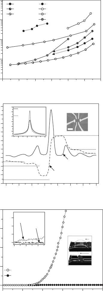
9.6 Electrical characterization of layer-by-layer transferred and HNO
3
-
doped graphene films. (a) Sheet resistances of transferred graphene
films using roll-to-roll (R2R) dry transfer method combined with
thermal release tapes and a PMMA-assisted wet transfer method. (b)
Comparison of sheet resistance from this research and transmittance
plots taken from other references. The dashed arrows indicate the
expected sheet resistances at lower transmittance. (c) Electrical
properties of a monolayer graphene Hall bar device in vacuum. Four-
probe resistivity (left inset) is measured as a function of gate voltage
in the monolayer graphene Hall bar shown in the right inset at room
temperature (solid curve) and T = 6 K (dashed curve). The QHE
effect at T = 6 K and B = 9 T is measured in the same device. The
longitudinal resistivity r
xx
and Hall conductivity s
xy
are plotted as a
function of gate voltage. The sequence of the first three half-integer
plateaux corresponding to u = 2, 6 and 10, typical for single-layer
graphene, are clearly seen. The Hall effect mobility of this device is
m
Hall
= 7350 cm
–2
V
–1
s
–1
at 6 K (~5100 cm
–2
V
–1
s
–1
at 295 K). Scale
bar (inset), 3 mm. (d) Electromechanical properties of graphene-based
touchscreen devices compared with ITO/PET electrodes under tensile
strain. The inset shows the resistance changes with compressive and
tensile strain applied to the upper and lower graphene/PET panels,
respectively. (From Ref. [2].)
than that of the PMMA-assisted wet transfer method. As the number of
layers increases, the resistance drops faster compared to the wet transfer
method (Fig. 9.6a). We postulate that the adhesion of the rst layer with the
substrate is not strong enough for complete separation of the graphene lms
from the thermal release tape. As a result, there can be mechanical damage
on the graphene lms, leading to an increase in the overall sheet resistance.
Because additional layers are not directly affected by the adhesion with the
substrate surface, the sheet resistance of multilayers prepared by the roll-
to-roll method does not differ much from that for the wet transfer case. The
p-doping with Hno
3
clearly enhances the electrical properties of graphene
ThinFilm-Zexian-09.indd 223 7/1/11 9:42:30 AM
224 Thin film growth
© Woodhead Publishing Limited, 2011
70 75 80 85 90 95 100
Transmittance (%)
(b)
Sheet resistance (W
–1
)
10
4
10
3
10
2
10
1
10
0
This work
This work
Theory
Ref. 6
Ref. 19
Ref. 25
Ref. 28
Wet-transferred
graphene
(ref. 19)
Graphene grown on Ni
Carbon nanotubes
R2R graphene
R2R graphene + doping
ITO (calculation)
Graphene (calculation)
9.6 Continued
1 2 3 4 5 6
Strain (%)
(d)
DR/R
0
DR/R
0
200
150
100
50
0
ITO
R2R graphene
3
2
1
0
Tensile
Compressive
0 2 4
Strain (%)
–30 –20 –10 0 10 20 30 40
V
bg
(V)
(c)
Magnetoresistance (kW)
30
25
20
15
10
5
0
–5
–10
–15
R (kW)
12
10
8
6
4
2
0
–20 0 20 40
V
bg
(V)
T=295K
T=6K
R
xx
R
xy
ThinFilm-Zexian-09.indd 224 7/1/11 9:42:31 AM
225Growth of graphene layers for thin films
© Woodhead Publishing Limited, 2011
lms, and is more effective in roll-to-roll processes. The sheet resistance of
the p-doped four-layer graphene lm with ~90% optical transmittance is as
low as ~30 W/sq, which is superior to common transparent electrodes such
as indium tin oxide (ITO) and carbon-nanotube lms (Fig. 9.6b).
26
Standard electron-beam lithography has been used to fabricate graphene
Hall bars on conventional 300 nm Sio
2
/Si substrates (Fig. 9.6c). The left
inset of Fig. 9.6c shows the four-terminal resistance of such samples as a
function of backgate voltage (V
bg
) at both room temperature (solid curve)
and at a low temperature (T = 6K) and zero magnetic eld. We observe the
graphene specic gate bias dependence of the resistance with a sharp Dirac
peak and an effective Hall mobility of 7350 cm
2
V
–1
s
–1
at low temperatures.
This allows the observation of the quantum Hall effect (QHe)
27
at 6K and
a magnetic eld of B = 9T (Fig. 9.6c, right). The ngerprint of single-layer
graphene, the half-integer quantum Hall effect, is observed with plateaux at
lling factors of u = 2,6 and 10 at R
xy
= 1/2, 1/6 and 1/10 (h
2
/e
2
), respectively.
Although the sequence of the plateaux remains for both the electron side
and the hole side, there is a slight deviation from the fully quantized values
on the hole side.
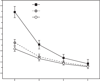
Finally, the electromechanical properties of graphene/PeT touchscreen
panels were tested (Fig. 9.6d). Unlike an ITo-based touch panel, which
easily breaks under ~2–3% strain, the graphene-based panel resists up to
6% strain; this is limited not by the graphene itself, but by the printed silver
electrodes (Fig. 9.6d).
28
9.4 Conclusions
In conclusion, we showed a method for graphene growth on nickel and copper
layers using chemical vapour deposition and further described a method to
transfer graphene lms to stretchable substrates. This will lead to numerous
applications including use in large-scale exible, stretchable, foldable
transparent electronics. In addition, given the scalability and processability
of roll-to-roll and CVD methods and the exibility and conductivity of
graphene lms, we anticipate that the commercial production of large-scale
transparent electrodes, replacing ITo, will be realized in the near future.
9.5 References
1. Hong, B. H. et al. Large-scale pattern growth of graphene lms for stretchable
transparent electrodes. Nature 457, 706–710 (2009).
2. Hong, B. H. et al. Roll-to-roll production of 30-inch graphene lms for transparent
electrodes. Nature Nanotech. 5, 574–578 (2010).
3. Yu, Q. et al. graphene segregated on ni surfaces and transferred to insulators. Appl.
Phys. Lett. 93, 113103 (2008).
4. Ferrari, A. C. et al. Raman spectrum of graphene and graphene layers. Phys. Rev.
Lett. 187401 (2006).
ThinFilm-Zexian-09.indd 225 7/1/11 9:42:31 AM
226 Thin film growth
© Woodhead Publishing Limited, 2011
5. obraztsov, A. n., obraztsova, e. A., Tyurnina, A. V. and Zolotukhin, A. A. Chemical
vapor deposition of thin graphite lms of nanometer thickness. Carbon 45, 2017–2021
(2007).
6. Khang, D.-Y. et al. Individual aligned single-wall carbon nanotubes on elastomeric
substrates. Nano Lett. 8, 124–130 (2008).
7. Yang, P. et al. Mirrorless lasing from mesostructured waveguides patterned by soft
lithography. Science 287, 465–467 (2000).
8. Li, X. et al. Highly conducting graphene sheets and Langmuir–Blodgett lms. Nature
Nanotechnol. 3, 538–542 (2008).
9. Eda, G., Fanchini, G. and Chhowalla, M. Large-area ultrathin lms of reduced
graphene oxide as a transparent and exible electronic material. Nature Nanotechnol.
3, 270–274 (2008).
10. nair, R. R. et al. Fine structure constant denes visual transparency of graphene.
Science 320, 1308 (2008).
11. Lewis, J. Material challenge for exible organic devices. Mater. Today 9, 38–45
(2006).
12. Sun, Y., Choi, W. M., Jiang, H., Huang, Y. Y. and Rogers, J. A. Controlled buckling
of semiconductor nanoribbons for strechable electronics. Nature Nanotechnol. 1,
201–207 (2006).
13. Khang, D.-Y., Jiang, H., Huang, Y. and Rogers, J. A. A stretchable form of single
crystal silicon for high-performance electronics on rubber substrates. Science 311,
208–212 (2006).
14 Lee, C., Wei, X., Kysar, J. W. and Hone, J. Measurement of the elastic properties
and intrinsic strength of monolayer graphene. Science 321, 385–388 (2008).
15. Li, X. et al. Large-area synthesis of high-quality and uniform graphene lms on
copper foils. Science 324, 1312–1314 (2009).
16. Li, X. et al. Transfer of large-area graphene lms for high-performance transparent
conductive electrodes. Nano Lett. 9, 4359–4363 (2009).
17. Hecht, D. S. et al. Carbon nanotube lm on plastic as transparent electrode for
resistive touch screens. J. Soc. Inf. Display 17, 941–946 (2009).
18. Hass, J. et al. Why multilayer graphene on 4H-SiC(000-1) behaves like a single
sheet of graphene. Phys. Rev. Lett. 100, 125504 (2008).
19. Sprinkle, M. et al. First direct observation of a nearly ideal graphene band structure.
Phys. Rev. Lett. 103, 226803 (2009).
20. Das, A. et al. Monitoring dopants by Raman scattering in an electrochemically top-
gated graphene transistor. Nature Nanotech. 3, 210–215 (2008).
21. geng, H.-Z. et al. Effect of acid treatment on carbon nanotube-based exible
transparent conducting lms. J. Am. Chem. Soc. 129, 7758–7759 (2007).
22. Schrivera, M., Reganb, W., Losterb, M. and Zettl, A. Carbon nanostructure-aSi:H
photovoltaic cells with high open-circuit voltage fabricated without dopants. Solid
State Commun. 150, 561–563 (2010).
23. Wu, J. et al. organic light-emitting diodes on solution-processed metal nanowire
mesh transparent electrodes. ACS Nano 4, 43–48 (2010).
24. Reina, A. et al. Large area, few-layer graphene lms on arbitrary substrates by
chemical vapor deposition. Nano Lett. 9, 30–35 (2009).
25. Cai, W. W. et al. Large area few-layer graphene/graphite lms as transparent thin
conducting electrodes. Appl. Phys. Lett. 95, 123115 (2009).
26. Lee, J.-Y., Connor, S. T., Cui, Y. and Peumans, P. Solution-processed metal nanowire
mesh transparent electrodes. Nano Lett. 8, 689–692 (2008).
ThinFilm-Zexian-09.indd 226 7/1/11 9:42:32 AM
227Growth of graphene layers for thin films
© Woodhead Publishing Limited, 2011
27. Cao, H. L. et al. electronic transport in chemical vapor deposited graphene synthesized
on Cu: Quantum Hall effect and weak localization. Appl. Phys. Lett. 96, 122106
(2010).
28. Cairns, D. R. et al. Strain-dependent electrical resistance of tin-doped indium oxide
on polymer substrates. Appl. Phys. Lett. 76, 1425–1427 (2000).
ThinFilm-Zexian-09.indd 227 7/1/11 9:42:32 AM