Henini M. Handbook of Self Assembled Semiconductor Nanostructures for Novel devices in Photonics and Electronics
Подождите немного. Документ загружается.

Quantum Dot Charge and Spin Memory Devices 479
remain rather simple [24] . The enhanced Coulomb interactions in QDs due to the strong con-
fi nement give rise to energy shifts between different occupancy states of the order of a few milli-
electronvolts. Each occupancy state of electrons and holes, such as the single exciton (1 X 1 e ),
bi-exciton (2 X 2 e ), charged exciton ( X
2 e 1 h , X
1 e ), etc. then have a unique tran-
sition energy. * Furthermore, since the Coulomb energy shifts are much larger than the homo-
geneous linewidth of each transition ( Γ
hom
1), each occupancy state can be optically selected
via the frequency of either the emitted photon or laser used to address the system. This property
underpins the use of QDs for a diverse range of applications in the fi elds of classical and quantum
information processing.
In order to experimentally observe the single particle non-linearities discussed above, one has
to probe single dots in isolation [25] . Otherwise the minimum energy scale that can be probed is
limited by the inhomogeneous linewidth of the ensemble ( Γ
inhomog.
20 50 nm). This necessity
is nicely illustrated in Fig. 15.2b , which compares PL recorded from an ensemble of InGaAs QDs
with data recorded from the same sample through shadow mask apertures [26] . In this experi-
ment, single dots could be isolated by performing luminescence measurements through submi-
cron diameter apertures in an opaque metal fi lm. This measurement followed many others which,
already at the beginning of the 1990s, provided the fi rst direct evidence for the discrete electronic
structure of QD nanostructures via spatially resolved optical studies of localized excitons in quan-
tum well nanostructures [27, 28] . Shortly after these fi rst studies, various groups reported simi-
lar results on different QD systems using confocal microscopy [28, 29, 30] , near-fi eld optics [31,
32] and cathodoluminescence [33] techniques. In the pioneering work of Brunner et al. [27, 28]
* As a further complication, transitions between quasi 0D orbital states in the dot and delocalized carriers in
the 2D wetting layer continuum can also provide an intrinsic continuum absorption background for energies
above the fundamental s–s transition [71] . This property is manifestly far away from the idea that such nanos-
tructures behave as artifi cial atoms, while other properties of the dots, such as the observation of excitonic
Rabi oscillations, fi rmly underscore the analogy between quantum dots and real atoms.
With Coulomb interactions
s-s
Energy
p-p
3X
s
3X
p
4X
p
2X
1X
Without Coulomb
1200
i
Single dot
T 10 K
~10 QDs
~10
7
QDs
1250 1300
Energy (meV)
PL intensity (arb. units)
1350 1400
Γ
h
Γ
i
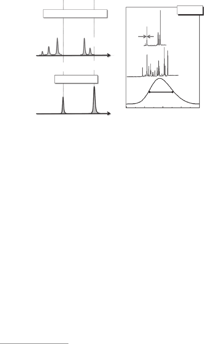
Figure 15.2 (a) Schematic representation of the form of the interband emission spectrum of a single QD without
(lower) and with (upper panel) Coulomb interactions between confi ned carriers. As discussed in the text, Coulomb
interactions lift the degeneracy of the orbital states allowing each occupancy state to be individually spectrally
addressed. (b) Photoluminescence spectra recorded at low temperatures from an ensemble of InGaAs QDs, revealing
a large inhomogeneous linewidth ( Γ
i
70 meV) and contrasting strongly with the homogeneous linewidth of a sin-
gle dot ( Γ
h
1 μ eV). The upper single dot spectrum also clearly shows the infl uence of Coulomb interactions on the
emission spectrum.
CH015-I046325.indd 479CH015-I046325.indd 479 6/24/2008 5:06:26 PM6/24/2008 5:06:26 PM
480 Handbook of Self Assembled Semiconductor Nanostructures for Novel Devices in Photonics and Electronics
the discrete and highly non-linear optical properties of single QDs were highlighted, together
with the possibility of controlling the spin of individual charge carriers via the optical polariza-
tion selection rules [27] . Studies of this type revealed that energy splittings between 1X and 2X
transitions typically lie in the range of a few millielectronvolts, with 2X lying either to lower or
higher energy than 1X, depending on the importance of direct Coulomb interactions and few
particle correlation effects [34] .
A further important development in the study and control of few particle states in QDs was
establishing an electrical contact to single dots. This provides the unique possibility to control the
QD charge occupancy using Schottky photodiode structures and has led to a number of advances
such as photocurrent absorption spectroscopy [35] , and the electrical detection of coherent opti-
cal control of excitons [36, 37] . The selective charging of self-assembled QDs was fi rst demon-
strated by Drexler et al. using capacitance spectroscopy of ensembles of InGaAs dots embedded in
the depletion region of a Schottky diode [38] . This was ingeniously extended by Warburton et al.
[39] , followed by other groups [39, 40, 41] , who combined this approach with near-fi eld opti-
cal spectroscopy through metal shadow masks to directly study the interaction of excitons with
additional electrons [39, 40] or holes [41] . These studies of charged excitons in QDs revealed a
wealth of information on Coulomb exchange and correlation effects in single dots populated by a
controlled number of charge carriers. Most recently, single dot absorption spectroscopy has been
shown to be a particularly clean method to directly probe the fundamental quantum properties
of excitonic transitions in QDs [42, 43] and even to facilitate measurement of the spin of a single
electron via spin state selective experiments [44] . An up-to-date overview of the fi eld of single
dot spectroscopy can be found in the proceedings of the biannual International Conferences on
Semiconductor Quantum Dots established in 2000, the most recent of which was held in May
2006 in Chamonix, France [45] .
15.1.3 Optical memory structures based on quantum dots
For the purpose of the present chapter, the single particle non-linearities discussed above play
an important role: they ensure that resonant optical excitation of QDs in the spectral range of
their s interband transition results only in the generation of a single electron–hole pair, the sin-
gle exciton, denoted by the nomenclature 1 X 1 e . Upon exciting an inhomogeneously broad-
ened ensemble with a narrowband source, one selects a subset of the dots from the ensemble via
their exciton transition frequency. Other excitations, such as 2 X 2 e X
1 e , X
2 e ,
etc. are detuned by many thousand linewidths from the exciton transition and are not excited via
any linear optical processes. In 1995 Shunchui Muto suggested that such an inhomogeneously
broadened ensemble of quasi zero-dimensional absorbing centres may be suitable for application
as an ultra-dense, wavelength domain, optical data storage medium [46] . The use of both spa-
tial and wavelength domains for data storage provide the potential to combine both high data
storage capacities ( 1 TB cm
2
) with very low switching energies. In this proposal, each bit of
information is represented by a small number of e h pairs, potentially even a single charge,
stored within an ensemble of QD nanostructures. High data storage densities are attainable since
data are stored in both spatial and frequency domains. One problem associated with the use of
interband excitations for frequency domain optical data storage is that they are relatively short
lived (typically ~1 ns) and electrically neutral, raising signifi cant problems related to the effi cient
detection of such optically encoded information. This limitation can be overcome by implement-
ing device concepts for separation of the optically generated e–h pair over timescales shorter than
the recombination lifetime, and then sensing these charges to read out the optically encoded
information.
Over the past ten years, these ideas have been explored by a number of groups with fi rst inves-
tigations focused on optical charge generation and non-selective electrical sensing of the stored
charge. In 1995 Yusa and Sakaki demonstrated an optically gated FET that incorporates a layer
of InAs QDs in the vicinity of a two-dimensional electron channel [47] . The observed photo-
switching operation of the channel resistivity in this device was attributed to the preferential
trapping of non-resonantly photo-generated holes in the dot layer. Finley et al. extended this
approach to conditions of resonant optical charge generation in the QD ground states and selective
CH015-I046325.indd 480CH015-I046325.indd 480 6/24/2008 5:06:26 PM6/24/2008 5:06:26 PM
Quantum Dot Charge and Spin Memory Devices 481
exciton ionization [48] . Later on, Shields et al. presented a similar scheme of electric readout in
nanoscale FET structures that eventually led to the observation of discrete photo-charging events
of individual QDs in the transport characteristics [49] . To date, a number of groups have shown
that single charges can be electrically [50, 51,52, 53] or optically [54, 55, 56] injected into QDs.
Alternatively, the quantum dots may be charged optically, an approach that, when combined
with wavelength selective writing or local probe techniques, could approach the situation where
each quantum dot stores a single bit of information as discussed in the introduction.
One of the crucial parameters for the use of InAs–GaAs QDs for optical memory applications
is the thermal activation barrier for the trapped carriers – the larger it is, the longer the storage
time becomes eliminating the need for frequent memory refresh cycles. Capacitance spectroscopy
has been shown to be a powerful method to investigate charge retention times [57] together with
deep-level transient spectroscopy and admittance spectroscopy for both InAs–GaAs [58, 59] and
Ge–Si QDs [60] . GaSb–GaAs dots have similar structural properties to the InAs–GaAs system, but
a signifi cantly larger hole ground state localization energy is expected due to the type II band
alignment attractive for holes [61] . The thermal activation barrier of hole-charged GaSb–GaAs
QDs has been studied by admittance spectroscopy and shown to provide extremely long hole stor-
age times, in excess of milliseconds even at room temperature [62] .
In the following sections we discuss the operation of early prototype optical charge memory
structures with electrical readout of the stored charge. These experiments are then contrasted
with devices that enable all optical charging and readout later in the chapter. These “ all opti-
cal ” memory devices provide a very convenient method to directly orientate the spin of the opti-
cally generated charges via the optical polarization selection rules. We then continue to describe
experiments in which we probe the electron and hole spin relaxation dynamics in self-assembled
QD nanostructures. The spin orientation is shown to be remarkably stable, demonstrating that
motional quantization dramatically suppresses spin relaxation via spin orbit interactions.
15.2 Optically induced charge storage
15.2.1 Electrical detection of stored charge
A number of groups have investigated the effects of a self-assembled InAs QD layer on the lat-
eral transport properties of a two-dimensional electron gas (2DEG) in MODFET-type structures
[51, 56, 63, 64] . These works have shown that the QDs can effi ciently act as controllable charge
traps and scattering centres which can be used to effectively tailor the transport properties of the
2DEG. Furthermore, several authors [51, 56] have demonstrated that such devices are strongly
photosensitive forming the foundation for a basic QD optical memory element or highly sensitive
QD phototransistor with single photon counting capabilities [65] .
15.2.1.1 Charge storage device structure
Optically induced charging of self-assembled InAs QDs has been studied in [48, 66] and using
an optically gated FET structure into which a layer of InAs quantum dots is embedded 50 nm
from a 2D electron or hole conducting channel. The operating principles of the devices are simi-
lar to a MODFET, as illustrated by Fig. 15.3a , with the exception that the metallic gate electrode
is replaced by a layer of self-assembled quantum dots that can be optically charged. By separat-
ing the 2D channel and QD layer using a wider band gap blocking barrier, photo-created excitons
can be selectively ionized leaving electrons (or holes) stored preferentially within the dots.
Figure 15.3b illustrates schematically the fundamental operating principles of these structures.
While the following discussion pertains to an electron storage device, the principles for holes, dis-
cussed below, are entirely analogous. The devices consist of a two-dimensional (2D) electron chan-
nel that was spatially separated by a blocking barrier from a layer of self-organized quantum dots
(upper panel of Fig. 15.3b ). The QD layer is embedded within the intrinsic region of a vertical p - i - n
junction. By fabricating separate ohmic contacts to both the 2D n -channel and buried p -contact,
the electric fi eld in the intrinsic region and conductivity of the n -channel ( σ ) can be tuned by
varying the DC bias applied to the p - i - n junction ( V
pn
). Following resonant optical excitation
CH015-I046325.indd 481CH015-I046325.indd 481 6/24/2008 5:06:27 PM6/24/2008 5:06:27 PM
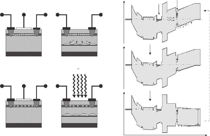
482 Handbook of Self Assembled Semiconductor Nanostructures for Novel Devices in Photonics and Electronics
of the quantum dots, the photo-created holes escape by thermal activation ( T 100 K) or by tun-
nelling ( T 100 K). By contrast, the electrons remain preferentially stored due to the presence of
the wider band gap-blocking barrier (middle panel of Fig. 15.3b ). The stored electrons within the
QD layer then selectively deplete the 2DEG, resulting in a reduction of its in-plane conductivity
which can be measured electrically. The magnitude of this conductivity change ( Δ σ ) is expected
to refl ect the charge density stored in the QDs. The stored electrons are then removed from the
QDs by forward biasing the vertical p - i - n junction (lower panel of Fig. 15.3b ). This results in the
injection of holes into the QD layer, where they become trapped by the dots, recombining radi-
atively with the stored electrons. The device then switches back to its initial state and another
charge write–store–reset cycle can be performed.
Devices similar to those illustrated in Fig. 15.3b have been grown on a [100] orientated semi-
insulated GaAs substrate and nominally consisted of the following epitaxial layers: 500 nm
p (Be) 2 . 1 0
18
c m
3
back contact followed by a 240 nm undoped (u.d.) GaAs spacer. After this,
2.25 ML of InAs was deposited at 530°C/0.04 MLs
1
which forms the self-assembled QDs. This
QD layer was capped with 5 nm GaAs before growth of the blocking barrier. This consisted of
30 nm undoped Al
0.3
Ga
0.7
As and a fi ve-period 2 nm(AlAs)/2 nm (GaAs) short period superlat-
tice to inhibit impurity segregation in the 2D electron channel. The 10 nm thick In
0.1
Ga
0.9
As
electron channel was then grown followed by a 40 nm-wide modulation-doped Al
0.3
Ga
0.7
As
barrier region. The modulation doping was incorporated into two narrow (1.5 nm) δ -doped
(~2 1 0
12
c m
1 2
) GaAs quantum wells in an effort to inhibit persistent photoconductivity asso-
ciated with carrier excitation from DX centres in the Al
0.3
Ga
0.7
As modulation-doped region [67] .
Finally, the sample was capped with 10 nm of n -doped (4 1 0
18
c m
3
) GaAs. A reference sam-
ple was also grown which was nominally identical to the above but without the QD layer. After
growth the wafers were processed into a Hall bar geometry using standard optical lithographic
techniques and separate ohmic contacts were established to both the 2D-electron channel and
the back p -contact to enable switching of the electric fi eld as depicted in Fig. 15.3 .
MODFET
(a) (b)
DotFET
Source
Source
Gate
Gate
Substrate
Substrate
Substrate
Substrate
Drain
Drain Drain
Stored
Writing
n-contact
2DEG
InAs-QDs
p-contac
t
CB
CB
VB
VB
VB
x
CB
eU
z
E
Γ
E
F
Erase
Drain
EnergyEnergyEnergy
Source
Source
2D
channel
QDs
V
Gate
0 V
V
Gate
0 V
hω
hω
IR
Figure 15.3 (a) Comparison of a conventional MOSFET and an optically switchable DotFET realized by embed-
ding a single layer of InGaAs quantum dots in the vicinity of a 2D conducting channel. (b) Schematic representation
of the device bandstructure and operating principles as discussed in the text.
CH015-I046325.indd 482CH015-I046325.indd 482 6/24/2008 5:06:27 PM6/24/2008 5:06:27 PM
Quantum Dot Charge and Spin Memory Devices 483
15.2.1.2 Demonstration of selective electron and hole generation
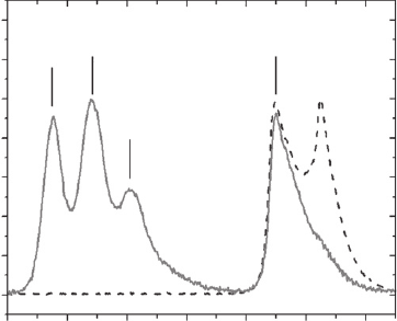
Figure 15.4 compares high power (5 Wcm
2
) ensemble PL spectra recorded from the sample
with QDs (sample A – full line) and the reference sample without dots (sample B – dashed line).
Over the energy range from 950 to 1200 meV a series of well-resolved peaks labelled E
n
, n 0 ,
1, 2 and 3 are observed which are separated by 64 3 meV and exhibit a linewidth (FWHM) of
35 meV. The energy at which these features arise together with their characteristic dependence
on the excitation power density identifi es them as arising from radiative recombination of s–s and
p–p transitions in the ensemble of QD ensemble studied. To higher energy, additional PL peaks
are observed which arise from recombination in the In
0.1
Ga
0.9
As quantum well (QW) and bulk
GaAs (GaAs) regions of the device. As expected, sample B (dashed line) generates no lumines-
cence over the energy range 800–1200 meV confi rming the absence of optically active centres.
In order to investigate optical charge storage effects a series of spectrally resolved photo-con-
ductivity measurements was performed. This consisted of a 100 s illumination period after which
the temporal dependence of the sample conductivity σ ( t ) was monitored before a reset electrical
pulse was applied to the p - i - n junction [68] . The excitation energy was then changed and the cycle
repeated. For these measurements the samples were held at T 145 K in a stabilized environment
designed to eliminate parasitic effects arising from ambient illumination and another persistent pho-
toconductive effect that was found to be present for T 100 K. Optical excitation was via a power-
stabilized quasi monochromatic white light from a tungsten halogen lamp ( P
max
1 mWcm
2
,
FWHM 5 meV) and the effect of exciting different quantum dots within the ensemble was studied
by tuning the excitation energy ( E
ex
) through the QD ensemble absorption spectrum.
Figure 15.5 shows σ ( t ) data obtained from sample A as a series of three illumination, recovery
and reset phases were performed with E
ex
1016 meV, 1024 meV and 1059 meV, respectively. The
onset of illumination is denoted by the label A, with the label B showing the point at which the
shutter is closed. The reset pulse is applied to the sample at C . The channel conductivity prior to
illumination is denoted by σ
0
, which for this sample was measured to be 1.5 0.2 mS. As can be
seen clearly in Fig. 15.5 , for E
ex
1016 meV the sample responds only weakly to illumination. By
contrast, after increasing E
ex
the photo-effect becomes much stronger until for E
ex
1020 meV a
rapid switching of σ is observed following illumination. We focus now on the illumination cycle at
E
ex
1059 meV [69] After closing the shutter (B) σ recovers weakly, saturating at a new level σ
2
.
Without resetting the sample, σ remained at σ
2
over timescales longer than eight hours at 145 K
while recovering towards σ
0
by less than 10%. This directly refl ects the potential for extremely long
charge storage times in the deep trapping potential of the quantum dots, even at elevated tem-
peratures. Sample B, which did not contain quantum dots, exhibited little or no photo-response,
independent of E
ex
, over the energy interval 900 meV E
ex
1200 meV [55] .
0.9 1.0 1.1 1.2
E
0
E
1
E
2
Energy (meV)
PL intensity (arb. units)
1.3 1.4
QW
GaAs
1.5
Figure 15.4 Photoluminescence spectra obtained at 293 K from the storage sample containing QDs (sample A – red
full curve) and the reference sample without QDs (sample B – dashed blue curve).
CH015-I046325.indd 483CH015-I046325.indd 483 6/24/2008 5:06:28 PM6/24/2008 5:06:28 PM
484 Handbook of Self Assembled Semiconductor Nanostructures for Novel Devices in Photonics and Electronics
Figure 15.6 shows the spectral dependence of the device photo-response for a number of one
shot measurements over the energy range 950 meV E
ex
1260 meV and for different reverse
biases applied to the vertical p - i - n junction (up to V
pn
2.5 V). The bold line shows the PL
spectrum obtained at 145 K for comparison. The onset of the photo-response discussed above is
very clearly observed for E
ex
1015 meV, fi rmly establishing the correspondence between the
observed photo-effect and charging of the lowest orbital states of selected quantum dots with a
1.80
1.60
1.40
1.20
0 250
V
pn
0.0 V
500 750
σ
2
σ
0
Δσ
1000
B
B
B
A
A
1.016 eV
145 K – Sample A
1.024 eV 1.059 eV
A
C
C
C
Time (s)
σ (mS)
Figure 15.5 Temporal dependence of the n -channel conductivity for the QD containing sample (A) as a series of
100 s illumination, recovery and reset cycles are performed as described in the text. The measurements were taken
with excitation energies of E
ex
1016 meV (leftmost), 1024 meV and 1059 meV (rightmost), respectively. The
arrows labelled A and B denote the points at which the illumination is applied and removed, respectively. The sample
is “ reset ” by forward biasing the p - i - n junction to neutralize the stored charge at point C. The reference sample (B)
showed a much weaker photo-response over the excitation range 900 E
ex
1200 meV indicating that the meas-
ured response arises from optically stimulated charge storage in the QDs.
160
145 K – Sample A
E
0
V
pn
A
0
A
1
A
2
E
1
140
120
100
% Δσ/σ
0
80
0.00 V
0.50 V
1.00 V
1.50 V
2.00 V
2.25 V
2.50 V
60
40
20
0
900 1000 1100 1200
Energy (meV)
1300
PL intensity (arb. units)
Figure 15.6 Spectral dependence of the photoconductive effect for sample A as a function of the reverse bias applied
to the vertical p - i - n junction from V
pn
0 to 2.5 V. The thick line shows a PL spectrum for comparison.
CH015-I046325.indd 484CH015-I046325.indd 484 6/24/2008 5:06:28 PM6/24/2008 5:06:28 PM
Quantum Dot Charge and Spin Memory Devices 485
single electron. Upon increasing V
pn
, the magnitude of the photo-effect increases strongly (up to
Δ σ / σ
0
100% for V
pn
2 . 5 V) refl ecting the electrostatic depletion of the n -channel under
reverse bias. The photosensitivity of the devices can be increased by depleting the 2D channel.
Over the same energy range, only a very weak photo-effect ( Δ σ / σ
0
5%) is observed from the ref-
erence sample. To higher energies, a series of peaks labelled A
0–2
are observed. Before discussing
these features, we note that the data plotted is the saturation value of the photo-response. Thus,
the magnitude of the charge storage observed includes all possible QD excitation mechanisms
regardless of the relative timescales over which they occur. The energy separation between A
0
and A
1
is 75 5 meV, much larger than the splitting between ground and excited quantum dot
peaks ( E
1
E
0
6 0 5 meV). Furthermore, these resonances are shifted from E
0
by 33 5 meV,
115 10 meV and 172 20 meV for A
0
, A
1
and A
2
, respectively. This indicates that they do not
simply refl ect direct optical charging of the ground and excited states of the quantum dots. These
observations were attributed to the participation of inelastic processes [55] over long timescales
involved, a superposition confi rmed by optical readout measurements discussed below. Following
direct excitation of the quantum dots ’ excited states, stored electrons are expected to relax rapidly
to the lowest orbital state [70] and multiple charging of the quantum dots may occur via the quasi
continuum absorption band of the QDs associated with crossed 2D–0D transitions [71] .
Similar experiments have also been performed on inverted devices in which holes are optically
stored in the QDs and sensed using a 2D In
0.1
Ga
0.9
As p -channel [72] . In all other respects the
device operating principles and fabrication are similar to the electron storage sample discussed
above. Besides being interesting from the fundamental physics viewpoint, hole storage may ena-
ble charge storage up to higher temperatures as a consequence of the larger effective mass, as
mentioned above [62, 73] . As for the electron storage sample discussed above the modulation
doped p -channel was separated by 50 nm from the InAs QD layer which was embedded within
the intrinsic region of a vertical n-i-p junction. The growth conditions for the QD layer were
nominally identical to the electron sample discussed above.
Figure 15.7 (inset) shows the photo-response of the hole storage sample following illumination
at E
ex
1050 meV, just above the peak of the ground state PL emission ( Fig. 15.7 – bold line, top
panel). As for the electron storage sample discussed above, a strong decrease ( Δ σ ) in the channel
0.4
HOLE STORAGE
T 145 K
V
pn
0.5 V
0.3
0.2
E
1
E
0
0.12
0.10
0.03
0 100 200 300 400
0.1
Δσ/σ
0
dσ/dt
0.0
0.7
0.6
0.5
0.4
0.3
0.2
800 900 1000
Time (s)
A
B
C
Δσ
Energy (meV)
1100 1200
σ(ms)
Figure 15.7 Inset: Persistent photoconductivity arising from optically stimulated hole storage in the QD layer (top
panel) QD charging spectrum for sample with (open squares) and without (open circles) the QD layer. (lower panel)
Switching rate spectrum ( d σ / dt ) for the hole storage sample at P
ex
0.02 mWcm
2
.
CH015-I046325.indd 485CH015-I046325.indd 485 6/24/2008 5:06:29 PM6/24/2008 5:06:29 PM
486 Handbook of Self Assembled Semiconductor Nanostructures for Novel Devices in Photonics and Electronics
conductivity was observed following illumination ( A ), which remains persistent for many hours
after closing the shutter ( B ). After resetting the device by forward biasing the n-i-p junction ( C )
the conductivity, once again, returns to the pre-illumination level ( σ
0
). A similar photo-response
is not observed in a separate reference sample, which did not contain quantum dots. Fig. 15.7
(top panel) shows the spectral dependence of the induced photo-effect Δ σ σ
0
for both QD (open
squares) and reference (open circles) samples, respectively. Since this data show the saturation
level of the photo-response, care should be exercised while interpreting the detailed form of the
charging spectrum. However, a clear onset is observed close to 1030 meV confi rming that the
photo-effect arises from hole storage within the quantum dots. Furthermore, the peaked struc-
ture observed in the Δ σ σ
0
data provides evidence for selective storage of holes within the QDs.
The fi lled squares in Fig. 15.7 (lower panel) show the spectral dependence of the device switch-
ing rate ( P
ex
0.05 mW/cm
2
) immediately after illumination for comparison. A series of peaks,
marked by the bold arrows on the fi gure, are clearly observed in d σ / dt arising close to the ground
and excited state PL emission from the QDs. This observation indicates that the observed persist-
ent photoconductivity arises from optically stimulated hole storage in the QDs.
The combination of the AlGaAs blocking barrier adjacent to the QD layer combined with the
switchable electric fi eld in the structure clearly enables charges to be selectively optically gener-
ated within a subset of self-assembled quantum dots. However, while the experiments discussed
above clearly demonstrate the ability to selectively generate charges within the ensemble of dots,
they cannot answer any the following questions:
● How many charges are generated per dot?
● What information does the spectral distribution of stored charge provide about the
response of a QD ensemble to quasi resonant optical excitation?
● What are the mechanisms by which stored charges are lost from the ensemble?
● Can these ideas be extended from optical charge generation to spin generation ?
To address these questions and reveal information about the optical charge storage process, fur-
ther experiments were performed with modifi ed devices that enable optical readout of the stored
charge.
15.2.2 Optically detected charge storage
The fi rst demonstration of full optical readout of optically induced charges was presented by
Lundstrom et al. , employing electric fi eld-induced charge transfer between a QD and a strain-
induced potential minimum in an adjacent quantum well [74] . Optical readout is vital since
spectral information about the stored charge distribution within the ensemble can be preserved
by optical detection schemes; the selective transfer of one of the photo-generated charge carri-
ers out of the QD does not destroy the energetic information encoded during the optical writing
process provided that the second carrier continues to reside in the dot where it was generated.
This is a vital ingredient of the optical memory scheme discussed in [46] . An exciton can then
be re-formed in the ground state of the same QD by subsequent back transfer of charge, leading
to photon emission from an identical quantum mechanical environment to that present during
the initial absorption process. The selective optical generation and readout of a single charge car-
rier in a zero-dimensional electronic environment is therefore a key requirement with regards to
preserving spatial and spectral information. Furthermore, as discussed later in the chapter it can
also provide information about thermally induced charge redistribution [77] and the ideas can
be extended from charge storage to spin storage [75] by utilizing the polarization degree of free-
dom of the excitation source.
We continue to discuss such a wavelength selective QD-based charge storage device with opti-
cally stimulated charge storage (electron or hole) and a demonstration of direct optical readout of
the stored charge distribution in the spectral domain. We will see that similar device concepts are
utilized to those discussed in the previous section, but spectral information is retained in the opti-
cal readout process. This provides further scope to investigate thermally induced charge redistri-
bution and, crucially, electron and hole spin relaxation as discussed in the fi nal sections of the
CH015-I046325.indd 486CH015-I046325.indd 486 6/24/2008 5:06:29 PM6/24/2008 5:06:29 PM
Quantum Dot Charge and Spin Memory Devices 487
chapter. Using these devices, wavelength domain “ data storage ” is demonstrated at T 10 K and
charges are stored over timescales much longer than 25 μ s. Analysis of the spectral distribution
of the stored charge enables the study of resonant and phonon-assisted absorption and, further-
more, temperature dependent measurements allow direct investigations of thermal carrier loss
from the QDs.
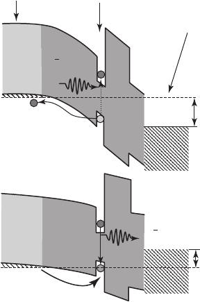
The operating principles and band diagram of a fully optical charge memory device are pre-
sented in Fig. 15.8 . A single layer of InGaAs QDs is embedded within the intrinsic region of either
an n - or p -type Schottky photodiode for hole or electron storage, respectively. In the following, we
describe the operation of the hole storage device, the principles for the electron storage sample
being entirely analogous. In the write mode ( Fig. 15.8a ), the device is reverse biased ( V V
store
).
Following resonant optical excitation of the QD sub-ensemble ( ω
aser
ω
write
), photo-generated
excitons are rapidly ionized by the strong vertical electric fi eld ( F ~ 150 kV/cm). While electrons
readily tunnel out of the dot, the holes remain stored by virtue of an AlGaAs barrier immedi-
ately adjacent to the QD layer. Providing that V
store
is chosen such that the exciton ionization
rate far exceeds the radiative lifetime, holes are effi ciently stored with a spectral distribution that
refl ects the response of the QD ensemble to resonant optical excitation. Optical readout of the
stored charge distribution is achieved by application of a forward bias pulse ( V V
reset
), resulting
in non-resonant injection of majority charge carriers into the QD layer and subsequent neutrali-
zation of the stored charge by radiative recombination. The resulting charge storage spectrum
directly refl ects the spectral distribution of stored charge within the QD ensemble.
CB
p-contact SAQDs
write
Initialization
Readout
Schottky
gate
eV
stor
e
eV
rese
t
VB
hω
read
hω
(a)
(b)
Figure 15.8 Schematic structure and operating principles of charge storage devices investigated. (a) In the charge
storage mode ( V
gate
V
store
) photon to charge conversion is ensured by the negative gate potential and selective exci-
ton ionization. (b) Conversion from charge to photon enabled by forward biasing the Schottky junction, hole reinjec-
tion and detection of the resulting storage EL at ω
read
ω
write
as discussed in the text.
As for the electrical memory devices discussed above, the optical memory structures were
grown using molecular beam epitaxy on [100] semi-insulating GaAs substrates. After an undoped
GaAs buffer, a back contact layer was deposited, consisting of 200 nm of heavily ( p - or n -)
doped GaAs ( N
D/A
10
18
c m
3
). Following this, a 50 nm-undoped GaAs buffer was grown followed
CH015-I046325.indd 487CH015-I046325.indd 487 6/24/2008 5:06:29 PM6/24/2008 5:06:29 PM
488 Handbook of Self Assembled Semiconductor Nanostructures for Novel Devices in Photonics and Electronics
by the QD layer that consisted of 6 ML of In
0.5
Ga
0.5
As, deposited at 520°C and 0.1 ML/s. These
growth conditions resulted in approximately lens-shaped QDs with a mean diameter (height)
of 25 nm (4 nm). Moreover, the optical activity of these QDs is such that the emission from
their fundamental transition is around ~950 nm and can be detected using high-sensitivity
silicon-based detectors. The dot density was ~150 μ m
2
measured by atomic force microscopy
on a sequentially grown control sample. The QDs were capped by 1 nm GaAs, a 50 nm thick
Al
0.4
Ga
0.6
As blocking layer and completed with 10 nm GaAs. The wafers were then processed
into photodiodes, with ohmic contacts established to the buried back contact and completed with
a 10 nm thick, semi-transparent, top Schottky contact.
All optical experiments discussed below were performed using a standard micro-photolumi-
nescence (PL) system and resonant optical excitation pulses were delivered using a mechanically
modulated continuous-wave (CW) Ti–sapphire laser ( ω
write
1.25–1.38 eV) or the Ti–sapphire
in combination with a laser diode ( ω
write
1.27 eV) for two colour experiments. An accurately
timed sequence of optical (write) and electrical (readout) pulses were applied to the sample at a
repetition rate of ~20 kHz.In order to ensure effi cient suppression of scattered laser light dur-
ing detection, an Si-based gated avalanche photodiode was used and only switched on during
application of the readout voltage pulse. The charge storage time ( Δ t ) is defi ned as the time delay
between switching off the optical write pulse and the onset of the electrical readout.
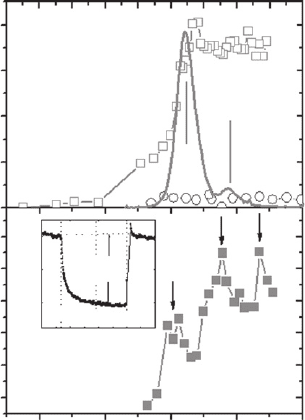
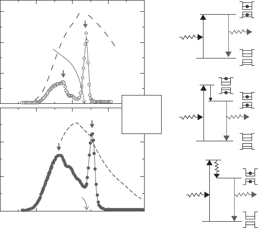
Typical charge storage spectra for electron (dashed line) and hole (solid line) devices are pre-
sented in Fig. 15.9a for a storage time of Δ t 1 2 μ s. The overall form of the charge storage
spectra was found to be very similar for both samples, consisting of two principal components:
a sharp peak, labelled R in Fig. 15.9a , very close to the excitation energy and a much broader
band, labelled S , ~20–50 meV to lower energy. For both samples, ω
write
was tuned to the high-
energy side of the QD ensemble (~1.27 eV – dashed line in Fig. 15.9a ) and the magnitude of the
readout voltage was
||V
reset
0.8 V corresponding to the onset of majority carrier current fl ow.
h
storage
1.15
Storage signal (arb. units)
1.20
1.25
1.30 1.35
Energy (eV)
R
E
L
E
L
E
L
E
S
E
1x
E
1x
E
1x
hω
1x
hω
1x
hω
1x
hω
L
hω
L
0
0
0
hω
L
E
p
E
ph
E
s
S
e
storage
R
S
hω
write
hω
write
(a)
(b)
(c)
(d)
Δt 12μs
B 0 T
T 10 K
Figure 15.9 (a) Typical emission spectra after application of the reset bias pulse ( Δ t 1 2 μ s), for electron (lower
panel) and hole (upper panel) storage devices, together with the non-resonantly excited QD ensemble luminescence
spectrum of the hole storage device (dashed lines). The absorption processes resulting in the resonant (R) and low
energy (S) emission features are also schematically depicted. (b) Ground state absorption giving rise to R. (c) Quasi-
resonant excitation via excited state generating the broad emission band S. (d) Phonon-assisted absorption generating
the peaks marked with S and arrows. Redrawn from [105] by permission of the American Physical Society.
CH015-I046325.indd 488CH015-I046325.indd 488 6/24/2008 5:06:30 PM6/24/2008 5:06:30 PM