Henini M. Handbook of Self Assembled Semiconductor Nanostructures for Novel devices in Photonics and Electronics
Подождите немного. Документ загружается.

Engineering of Quantum Dot Nanostructures for Photonic Devices 509
where
E
Q
D
0
is the energy gap of unstrained material and:
δε
δε
δε
Ea
Ea
Eb
v
cch
Hh
Sb
⫽
⫽
⫽
(16.5)
where a
c
, a
v
and b are the hydrostatic deformation potentials of conduction band and valence
band and shear one, respectively.
Therefore, we can conclude that the CL composition x and the LCL thickness t are available to
change the QD strain and then the energy gap of the QD material; E
QD
as well as the x -dependent
band discontinuities can be used as two design parameters that determine the QD emission
energy. The relevant consequences of the QD strain engineering [34] approach in designing QD
structures will be discussed in section 16.3.2.
16.3.1 The quantum dot strain engineering approach: experimental
Experimental confi rmations of the effect of the InGaAs LCL thickness on the emission energy of
overlying InAs QDs, provided by photoluminescence (PL) studies of MBE-grown metamorphic
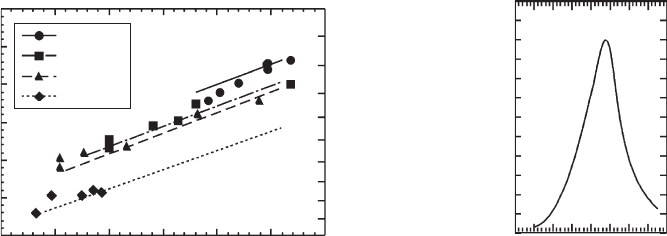
InAs/InGaAs nanostructures [34, 38] , are presented in Fig. 16.2a . The symbols correspond to
10 K peak emissions for 3 ML InAs QDs embedded in InGaAs CLs, plotted as a function of the
QD–CL mismatch f (depending on the LCL thickness t ) for different CL compositions x . The results
show that the emission is red shifted by the reduction of f (i.e. by the decrease of the QD strain),
alongside with the increase of x [34] .
From atomic force microscopy (AFM) characterization of uncapped structures it was found
that the QD height distribution (peaked at 4 ⫾ 1 nm) is scarcely dependent on x and f , while the
value of the most frequent QD diameter (21 ⫾ 4 nm) is almost constant for x ⱕ 0.33, but dramat-
ically increases up to 29 ⫾ 4 nm for x ⫽ 0.35; on the contrary, diameters are basically unaffected
by the QD–CL mismatch. As for capped structures, we do not expect intermixing and segregation
effects [19, 26, 32] that could modify QD sizes, since our QDs and UCLs are purposely grown by
ALMBE at relatively low temperatures (460°C and 360°C, respectively). All these observations
allow us to conclude that the red shift of QD emission energy due to the reduction of the mis-
match is caused only by the decrease of QD strain.
The right-hand side axis in Fig. 16.2a refers to the expected wavelength of radiation that would
be generated at RT from structures emitting at 10 K at the energies given on the left-hand side scale;
Figure 16.2 (a) 10 K PL emission energy (left vertical scale) and expected RT emission wavelength (right scale)
as functions of QD–CL mismatch in InAs/In
x
Ga
1 ⫺
x
As QD strain engineered structures. The wavelength scale
is obtained from the energy one by taking into account the Varshni shift from 10 K to RT. The lines represent the
results of the model calculations. (b) RT emission spectrum peaked at 1.44 μ m, from a structure with x ⫽ 0.24
and t ⫽ 145 nm ( f ⫽ 0.0592), not shown in panel (a). The excitation power density is 5 W/cm
2
. Reprinted with
permission from [38]. Copyright 2007, American Institute of Physics.
1.100
1.050
1.000
0.950
10 K PL emission energy (eV)
0.900
0.850
0.800
(a)
1.25
1.30
1.35
1.40
1.45
1.50
1.55
1.60
1.65
1.70
0.045 0.050 0.055 0.060
QD–CL mismatch
Expected RT emission
wavelength (μm)
0.065 0.070
10 K
x ⫽ 0.15
x ⫽ 0.28
x ⫽ 0.31
x ⫽ 0.35
1.0
RT
0.8
0.6
0.4
0.2
0.0
1.20
(b)
PL intensity
1.30 1.601.501.40
Wavelength (μm)
CH016-I046325.indd 509CH016-I046325.indd 509 6/25/2008 3:16:18 PM6/25/2008 3:16:18 PM
510 Handbook of Self Assembled Semiconductor Nanostructures for Novel Devices in Photonics and Electronics
the expected RT wavelength scale has been calculated from the measured 10 K emission energy one
considering a Varshni [50] shift of 70 meV when increasing the temperature from 10 K to RT. It is
worth noting that the QD emission energy could be shifted down to values that would correspond
to wavelengths beyond the 1.55 μ m region at RT, if the emission were not quenched. However,
due to the signifi cant thermal quenching of PL emission (to be discussed below) for In-rich CLs,
the longest emission wavelength observed at RT under low excitation power density (5 W/cm
2
) was
1.44 μ m, for a structure with x ⫽ 0.24 and f ⫽ 0.0592 ( Fig. 16.2b ).
Lines in Fig. 16.2a represent calculations of QD ground state emissions provided by a model
that will be presented and discussed in depth in section 16.3.2. It is noticeable how these cal-
culations and experimental results agree quite satisfactorily with discrepancies not larger than
25 meV, which can be accounted for by uncertainties in QD sizes as measured by AFM and by
approximations in the model and in its input parameters. This agreement confi rms the conclu-
sions made on the relevance of QD strain reduction to red shift the emission.
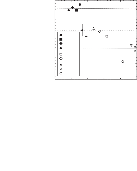
The model can be used to design structures emitting at predetermined wavelengths by select-
ing the appropriate pairs of x and t ; indeed, Fig. 16.3 [36] presents the experimental PL emission
energies at 10 K (symbols) of structures with values of x and t calculated by the model in order to
have RT emission at the wavelengths of 1.3, 1.4, 1.5 and 1.55 μ m; the dashed lines are drawn at
the 10 K emission energies corresponding to the indicated RT wavelengths. The horizontal error
bar represents the ⫾ 3% error in mismatch that may stem from the uncertainty in the RHEED
calibrations of In and Ga fl uxes, while the vertical bar on model calculations refers to errors of
⫾ 4 nm and ⫾ 1 nm for the most frequent values of the QD diameter and height, respectively.
Once again, the agreement between experimental results and model calculations is satisfactory,
thus showing how our model can be used to predict the experimental values of QD emission at
low temperatures, where quenching effects are irrelevant.
1.050
1.000
0.950
0.900
10K emission energy (eV)
0.850
0.800
0.075 0.070 0.065 0.060
1.55 μm @ RT
1.5 μm @ RT
1.4 μm @ RT
1.3 μm @ RT
QD–CL mismatch
0.055 0.050
x ⫽ 0.09
x ⫽ 0.12
x ⫽ 0.15
x ⫽ 0.18
x ⫽ 0.24
x ⫽ 0.28
x ⫽ 0.31
x ⫽ 0.33
x ⫽ 0.35
Figure 16.3 10 K PL emission energies (symbols) as functions of the QD–CL mismatch in InAs/In
x
Ga
1 ⫺
x
As
structures with ( x, f ) pairs selected for expected 1.3, 1.4, 1.5 and 1.55 μ m RT emission. The dashed lines are drawn
at 10 K emission energies corresponding to the RT wavelengths shown in the figure. Reprinted with permission from
[36]. Copyright 2005, American Institute of Physics.
Thermal quenching of the QD emission intensity is caused by the increased effectiveness of
non-radiative mechanisms for confi ned carrier loss, in competition with radiative recombination.
By fi tting the equation:
I
I
a E kT b E kT
⫽
⫹⫹
0
12
1 exp( / ) exp( / )−−
(16.6)
CH016-I046325.indd 510CH016-I046325.indd 510 6/25/2008 3:16:18 PM6/25/2008 3:16:18 PM
Engineering of Quantum Dot Nanostructures for Photonic Devices 511
to the temperature ( T ) dependence of the photoluminescence integrated intensity ( I ) it is possible
to derive the values of the activation energies E
1
and E
2
of two different quenching processes. As
discussed in [51, 52] , the non-radiative process related to the larger activation energy E
1
is the
confi ned carrier thermal escape from QD levels, whose activation energy is given by the sum of
the energy differences between the fi nal levels of the escape process (such as CL ones) and that
of QDs for both electrons and holes. The smaller activation energy E
2
may be related to extrinsic
processes likely caused by defects in the structures [53, 54] .
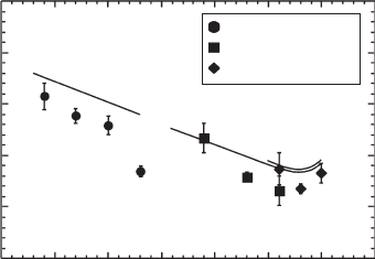
To investigate channels where confi ned carriers escape to, the experimental values of E
1
can
be compared with the sum of the energy differences of QD and CL states for electrons and heavy
holes, as calculated by our model. In Fig. 16.4 [36] values of activation energies E
1
for structures
of Fig. 16.3 obtained both by model calculations and by fi tting Eq. 16.6 to the experimental data
are plotted as functions of CL composition as lines and symbols, respectively. Both experimen-
tal and model values decrease as x increases; an effect that can be easily understood in terms of
shrinking band discontinuities between QDs and CLs and that will be discussed in more depth in
section 16.3.2.
500
400
300
Activation energy (meV)
200
100
0
0.05 0.10 0.15 0.20 0.25
1.5 μm
1.4 μm
1.3 μm
LCL composition
0.30 0.35 0.40
1.3 μm structures
1.4 μm structures
1.5 μm structures
Figure 16.4 Experimental (symbols) activation energies for PL thermal quenching as a function of the CL composition
x of InAs/In
x
Ga
1 ⫺
x
As structures designed for expected 1.3, 1.4 and 1.5 μ m operation at RT. Lines represent results of
model calculations. Reprinted with permission from [36]. Copyright 2005, American Institute of Physics.
A second important observation is that the measured E
1
values fall consistently below the
model ones; this has been explained by assuming that the fi nal states of the escape process are
wetting layer (WL) rather than CL ones, interpretation that was supported by the photorefl ect-
ance study of the same structures that evidenced the occurrence of transitions to WL states [38] .
The smaller activation energy E
2
has values in the 30–70 meV range and is caused by extrin-
sic processes such as non-radiative recombinations due to defects [36, 54] or losses of photogen-
erated carriers in confi ning layers [53, 55] .
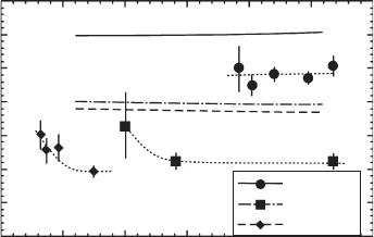
The dependence of activation energies E
1
on the QD–CL mismatch f deduced from experi-
ments (symbols) and model calculations (lines) for some structures of Fig. 16.2 is presented in
Fig. 16.5 . As in Fig. 16.4 , model calculations considering CL states as escape channels predict
values 50–90 meV above those derived from the fi tting of PL integrated intensity data.
16.3.2 The quantum dot strain engineering approach: model and discussion
As mentioned in the previous section, a simple and yet effective model was developed to calculate
QD ground state emission in strain engineered structures [34, 38] . It is based on a single-band,
effective-mass approach for QDs with cylindrical symmetry, following the work of Marzin and
Bastard [56] . Although a large number of more refi ned and complex models have been presented
in the literature, including four-band [57] and eight-band [58] k ⭈ p treatments, pseudopoten-
tial [59] and Green function deterministic numerical methods [60] , it has been pointed out in
CH016-I046325.indd 511CH016-I046325.indd 511 6/25/2008 3:16:19 PM6/25/2008 3:16:19 PM
512 Handbook of Self Assembled Semiconductor Nanostructures for Novel Devices in Photonics and Electronics
[58, 60] that such a simpler approach is more suitable for the description of fundamental transi-
tions in QDs, as those under consideration here. For a comprehensive review of theoretical work
on QD modelling, we refer the reader to [61] .
We considered QDs with truncated conical shapes and with base diameters and heights given
by the most frequent values in the respective distributions derived by AFM characterization of
uncapped structures; values of the ratio between base and top diameters were taken similar
to those reported in the literature (2.5–3.0) [62, 63] . The composition of QDs was considered
uniform and equal to the nominal one; this assumption is justifi ed since, as discussed in section
16.3.1, the relatively low growth temperatures of QDs and UCLs are expected to limit segregation
and interdiffusion of elements.
The band discontinuities between QDs and CLs were calculated according to the model solid
theory (MST) [64] , inclusive of strain effects. The MST parameters of InGaAs were deduced from
those of the binary constituents as proposed by Cardona and Christensen [65] , while the effective-
mass values (in units of free electron mass) for InAs QDs were taken as 0.04 for electrons, to
include the effect of strain, and 0.59 for heavy holes [57] . The values of other parameters such
as elastic constants and electronic band structure ones were taken from the recent literature
[66] . The binding energy of excitons was assumed to be 20 meV [67] .
The calculation of the hydrostatic and biaxial components of the QD strain, determining
the band-edge profi les of QDs and CLs, were carried over following the analytical approach of
Andreev et al. [47] , where values for InAs QDs embedded in GaAs are given as linear functions
of the QD–CL mismatch. While the hydrostatic strain is constant inside the QDs, the biaxial
one is position dependent, therefore we have taken an average value derived from the results of
[47, 68] ; in particular, we assumed the value of 0.05 for InAs QDs in GaAs confi ning layers and
scaled the value for InAs QDs in InGaAs CLs. Finally, the biaxial component of strain in the CLs
induced by the presence of QDs was disregarded.
The Schrödinger equation for electrons and heavy holes was solved considering both the QD
and a 1.6 ML thick WL as included in a cylindrical box larger than the QD; the envelope func-
tions of carriers were written in terms of a complete orthonormal set of eigenfunctions of the
box [56] . Then, the Schrödinger equation was transformed in a system of linear algebric equa-
tions, which were solved with well-known computational techniques.
The experimental data of Figs 16.2–16.5 proved that model calculations are indeed accurate
in predicting the dependence of emission energy and activation energy of carrier thermal escape
on the two design parameters, the CL composition x and the QD–CL mismatch f . Thanks to this
experimental validation, a deeper analysis of model calculations can provide a more quantitative
insight on the fundamental features of QD strain engineering and may allow for a rationalization
of our and literature experimental data.
350
300
250
200
Activation energy (meV)
150
100
50
0
0.045 0.050 0.055 0.060
QD–LCL mismatch
InAs/In
x
Ga
1⫺x
As QDs
metamorphic LCL
0.065 0.070 0.075
x ⫽ 0.15
x ⫽ 0.28
x ⫽ 0.35
Figure 16.5 Activation energies for PL thermal quenching as a function of the QD–CL mismatch. The dotted lines
are guides for the eye, while continuous, dashed and dotted–dashed lines represent the results of model calculations.
Reprinted with permission from [38]. Copyright 2007, American Institute of Physics.
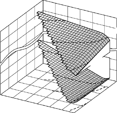
The upper surface in Fig. 16.6 represents the calculated 10 K emission energy of QDs as a func-
tion of x and f [38] , while the lower one represents the sum of the energy differences between
CH016-I046325.indd 512CH016-I046325.indd 512 6/25/2008 3:16:19 PM6/25/2008 3:16:19 PM
Engineering of Quantum Dot Nanostructures for Photonic Devices 513
QD and CL states for electron and heavy holes; this quantity corresponds to the activation energy
for thermal escape of confi ned carriers from QD to CL states. The surfaces have been drawn only
for values of ( x, f ) pairs that correspond to in-plane LCL residual strain ε
res
larger than 0.002,
the minimum value for which the Marée et al. model is considered reliable [41] . The dashed lines
on the ( x, f ) plane indicate the ( x, f ) pairs of structures expected to have RT emission at 1.3, 1.4
and 1.55 μ m; these lines are also projected on the upper surfaces. As already discussed when pre-
senting Fig. 16.3 , it was experimentally proved [36] that structures designed with such values of
x and f showed a satisfactory agreement between predetermined and measured values of emis-
sion wavelengths. The sharp decrease of emission energy when x increases beyond 0.33 is due
to the abrupt change of QD diameters that was discussed in section 16.3.1; due to the sudden
widening of the QD potential well, electron and hole confi nement energies decrease, resulting in
an additional red shift of the QD emission. The same argument also explains the slight increase
of the activation energies for x ⱕ 0.33, which is noticeable in Fig. 16.6 and in the experimental
data of Fig. 16.4 .
Looking at Fig. 16.6 it can be clearly seen that in the QD strain engineering approach the QD–
CL mismatch and the CL composition can be considered as two degrees-of-freedom that allow
the engineering of both the emission energy and the activation energy E
1
for thermal escape of
carriers from QDs. Let us consider, for example, the ( x, f ) pairs corresponding to RT emission at
1.4 μ m: by choosing pairs at the high- or at the low- x side of the dashed line relatively low or
high values of E
1
are obtained, respectively, which are about 170 and 250 meV, while the emis-
sion wavelength at RT in both cases is 1.4 μ m. It is worth noting that the longest emission wave-
length obtained so far (1.44 μ m, section 16.3.1) is from structures with ( x, f ) pairs lying in the
low- x side of the ( x, f ) plane.
Very interestingly, Figs 16.6 and 16.4 also show that structures expected to emit at 1.55 μ m
at RT have an inevitably small E
1
( ⬃ 180 meV) which hampers the achievement of RT operation,
unless different design criteria of structures are introduced (section 16.3.3).
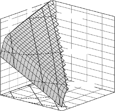
Figure 16.7 shows the 10 K emission energy from strain-engineered InAs/InGaAs structures
as a function of x and f ; the dashed lines represent ( x, f ) pairs of structures that would emit at
RT at the wavelengths indicated, while the thick continuous lines both on the ( x, f ) plane and
on the surface show the relationship that exists between x and f in structures with given values
of the thickness t of the lower CL. The Figure can be useful to illustrate the difference between
1.100
1.3 μm
1.000
0.900
0.800
0.400
Energy (eV)
0.300
E
E
act
0.200
0.100
0.05
0.10
0.15
0.20
CL composition
0.25
0.30
1.55 μm
1.4 μm
0.35
0.055
0.065
QD–CL mi
smatc
h
0.075
Figure 16.6 Calculated PL emission energy at 10 K (upper surface) and activation energy E
1
for thermal escape
of carriers ( E
act
lower surface) as functions of the QD–CL mismatch f and the CL composition x . The dashed lines
represent the ( x, f ) pairs that are expected to result in RT emission at the indicated wavelengths. Reprinted with
permission from [38]. Copyright 2007, American Institute of Physics.
CH016-I046325.indd 513CH016-I046325.indd 513 6/25/2008 3:16:20 PM6/25/2008 3:16:20 PM
514 Handbook of Self Assembled Semiconductor Nanostructures for Novel Devices in Photonics and Electronics
the usual design criteria followed in the literature and that proposed by QD strain engineering.
In the former case, only x is used to tune the emission wavelength, while t is not considered as a
design parameter. In this case, at the value of x determined in such a way only a defi nite value
of the activation energy for thermal escape of carriers results. Instead, in the case of QD strain
engineering x and the t -dependent f can be used to engineer two different parameters that are
emission and activation energies, thus allowing the maximization of the emission effi ciency at
predetermined operation wavelengths.
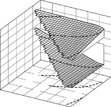
A more general understanding of the dependence of signifi cant parameters of the structure
on x and f can be reached by studying how the energy gap of the QD material E
QD
and the sum
Δ E of band discontinuities for electrons and heavy holes depend on the two design parameters
under consideration. Such quantities have been calculated by our model and are plotted in Fig.
16.8 [38] , where the upper and the lower surfaces represent E
QD
and Δ E . As in Fig. 16.6 , dashed
lines indicate the couples of values ( x, f ) of structures that should emit at 1.3, 1.4 and 1.55 μ m
at RT.
The slight dip in E
QD
for x ⱖ 0.33 is due to the increase in QD lateral sizes which modifi es the
dependence of the QD strain on QD–CL mismatch, as discussed in [47] . This causes also a reduc-
tion in the slope of Δ E.
It can be seen that the effect of the QD–CL mismatch on the energy gap is quite relevant, while
the CL composition for x ⬍ 0.33 has hardly any effect on it. On the other hand, the sum of the
band discontinuities depends strongly on the CL composition x and is basically unaffected by the
mismatch f .
From all above considerations, a qualitative understanding of this approach is possible by con-
sidering the following simple arguments: (i) the energy gap of strained InAs depends only on the
QD–CL mismatch and is basically unaffected by the CL composition (unless this parameter causes
changes in QD morphology), (ii) the sum Δ E of the band discontinuities, given by the difference
between the energy gap of CL and QD material, depends on x as only the energy gap of InGaAs
CLs has such a dependence and (iii) Δ E is essentially independent of f as both the CL and QD
energy gaps have a quite similar dependence on mismatch.
1.040
10 nm
30 nm
100 nm
300 nm
1.3 μm @ RT
1.4 μm @ RT
1.5 μm @ RT
1.020
1.000
0.980
0.960
0.940
10 K emission energy (eV)
0.920
0.900
0.880
0.860
0.840
0.070
0.065
QD–CL mi
smatc
h
0.060
0.055
0.30
0.20
CL compo
sitio
n
0.10
0.05
Figure 16.7 Calculated PL emission energy (10 K) as a function of the QD–CL mismatch f and the CL composition x .
The dashed lines represent the ( x, f ) pairs that are expected to result in RT emission wavelengths at 1.3, 1.4 and
1.5 μ m. The continuous lines show the ( x, f ) relationship for structures with given values of LCL thickness.
CH016-I046325.indd 514CH016-I046325.indd 514 6/25/2008 3:16:21 PM6/25/2008 3:16:21 PM
Engineering of Quantum Dot Nanostructures for Photonic Devices 515
A different perspective on the QD strain engineering approach can be gained by considering
the QD material (strained σ -InAs) as a “ virtual ” semiconductor material with its own lattice
parameter and energy gap represented in Fig. 16.9a by points on the dashed line labelled σ -InAs.
Instead, the closed circles and the continuous lines represent free-standing III–V binaries and
ternaries, respectively. From the Figure it can be noted that by increasing the lattice parameter
of strained InAs ( σ - InAs) from that of GaAs towards the InAs one E
QD
is red shifted according to
Eqs 16.4 and 16.5 .
Figure 16.9b , which is a blow-up of Fig. 16.9a , shows that E
QD
slightly depends also on QD
morphology, as mentioned above when discussing features of Fig. 16.8 : for x ⫽ 0.05–0.30 the
lines representing the energy gap of σ -InAs lean one on the other, while for x ⫽ 0.35 the line sets
at a smaller energy since for larger dots the material is slightly less compressed as the proportion-
ality constant between QD strain and QD–CL mismatch changes [47] .
The shaded area denoted by CL in Fig. 16.9a and the lines labelled σ -InGaAs and CL in Fig.
16.9b represent the metamorphic CLs with different composition in the 0.05–0.35 range. From
Fig. 16.9a it can be seen that the use of strain to shift the energy gap of the QD material can
be considered as an alternative approach as compared to the change of QD composition. In the
fi gure the arrows (labelled InNAs, InAsSb, InGaAs and σ ) diverging from the point representing
σ -InAs pseudomorphic on GaAs show, respectively, the effects of the introduction of N, Sb and
Ga in the InAs lattice and that of the reduction of strain in σ -InAs.
As a matter of fact, the use of In(Ga)AsN QDs has already proved to be a possible path towards
the extension of QD emission in the 1.55 μ m window [69–75] . On the other hand, InAsSb QDs
have been attracting relatively less attention, despite the fact that incorporation of antimony in
InAs QDs has shown promising properties both in terms of QD emission red shifting [76–78] and
improved QD growth [78–80] . On the other hand, the use of InGaAs to blue shift the QD emis-
sion energy is a well-established method, allowing for 0.98 μ m emission from QD structures, as
will be thoroughly discussed in section 16.4. The resort to ternary or quaternary alloys instead of
InAs for QDs, however, may present some elements of concern, such as the possible lower mate-
rial quality and the critical control of compositions; therefore further research work could help
clarify advantages and drawbacks of different QD materials. In any case, QD strain engineering
0.900
0.800
ΔE
E
QD
0.700
0.600
0.500
Energy (eV)
0.400
0.300
0.200
0.100
0.05
0.10
0.15
0.20
CL compo
sitio
n
0.25
0.30
0.35
0.055
1.3 μm
1.4 μm
1.55 μm
0.065
QD–CL mi
smatch
0.075
Figure 16.8 Calculated energy gap of the QD material (strained InAs) (upper surface) E
QD
and sum of band
discontinuities for electrons and holes Δ E (lower surface) as functions of the QD–CL mismatch f and the CL
composition x in InAs/In
x
Ga
1 ⫺
x
As QD strain engineered nanostructures. The dashed lines represent the ( x, f )
pairs that are expected to result in RT emission at the indicated wavelengths. Reprinted with permission from [38].
Copyright 2007, American Institute of Physics.
CH016-I046325.indd 515CH016-I046325.indd 515 6/25/2008 3:16:22 PM6/25/2008 3:16:22 PM
516 Handbook of Self Assembled Semiconductor Nanostructures for Novel Devices in Photonics and Electronics
and the use of multinary QDs are not mutually exclusive approaches and advantage can be taken
of the former solution to limit the incorporation of Sb and N in QDs that would be necessary to
obtain a predetermined red shift.
Figure 16.9 shows once more the quintessential features of QD strain engineering already evi-
denced by Figs 16.6 and 16.8: (i) the QD emission can be red shifted by decreasing the strain of
QDs in metamorphic structures; (ii) the increase in x composition of CLs can also contribute to
Figure 16.9 (a) Lattice parameters as functions of energy gaps for III–V binaries (closed circles) and ternaries
(continuous lines). The dashed line labelled σ -InAs represents the strained InAs (QD material). The shaded area
labelled CL indicates metamorphic CLs in QD strain engineered nanostructures. Arrows represent the effect of change
in composition of QDs from InAs to ternary materials (InAsSb, InNAs and InGaAs), and the effect of reduction of
strain for InAs QDs (labelled σ ). (b) Blow-up of (a) showing lattice parameters as functions of energy gaps for InAs
QDs and In
x
Ga
1 ⫺
x
As CLs under metamorphic regime (dashed lines) in structures with different values (0.05–0.35)
of the CL composition x .
0.62
0.61
0.60
0.59
0.58
Lattice parameter (nm)
0.57
0.56
0.55
0.54
(a)
300 K
GaNAs
InNAs
QD
InAsSb
InGaAs
σ-InAs
InNAs
InAsSb
InAs
InP
InGaP
InGaAs
GaAs
CL
0.0 0.5 1.0
1.55 1.31 0.98 0.92
Energy gap (eV)
Wavelength (μm)
1.5
σ
0.61
0.60
0.59
0.58
Lattice parameter (nm)
0.57
0.56
0.3 0.5 0.7 0.9 1.1 1.3
Energy gap (eV)
1.5
10 K
QD
InAs
σ-InAs
InGaAs
0.35
σ-InGaAs
0.30–0.05
0.25
0.35
0.15
0.05
GaAs
(b)
CL
CH016-I046325.indd 516CH016-I046325.indd 516 6/25/2008 3:16:23 PM6/25/2008 3:16:23 PM
Engineering of Quantum Dot Nanostructures for Photonic Devices 517
red shift the emission through the reduction of band discontinuities and then of confi nement
energies, but – concomitantly – it reduces the activation energy for carrier thermal escape and,
then, the RT emission effi ciency. A further comment, which only marginally emerges from Fig.
16.9 , is: (iii) the increase of QD sizes can be instrumental for the red shift of emission, as it was
done in the literature [8, 32] , since confi nement energies decrease while the activation energy
and, hence, the emission effi ciency increase.
16.3.3 Further steps towards QD emission at 1.55 μ m at room temperature
As discussed in the comments to Figs 16.4–16.8 , QD strain engineered structures designed for
long wavelength operation suffer a consistent reduction of the activation energy for thermal
escape of carriers ( E
1
⬃ 180 meV), which inevitably implies a smaller emission effi ciency at RT.
Indeed, to red shift the QD light emission in the 1.55 μ m region it is necessary: (i) to increase
the values of the CL composition in order to decrease the carrier confi nement energies and/or
(ii) to decrease the energy gap of the QD material by decreasing the QD strain. However, point
(i) implies the deleterious consequence of the reduction of QD–CL band discontinuities and,
hence, the decrease of the activation energy, while point (ii) can be pursued only to a limited
extent since the decrease of QD–CL mismatch ( Fig. 16.1 ) and that of QD strain saturates with
increasing t . These considerations explain why, as it has been already pointed out, the longest
wavelength experimentally observed at RT under low excitation conditions (5 W/cm
2
) is 1.44 μ m
[38] , in spite of the fact that emission at much longer wavelength could be obtained if transitions
were not quenched ( Figs 16.2 and 16.3 ). A modifi cation of the structure is hence necessary to
get QD emission at RT in the 1.55 μ m region.
An interesting option is provided by embedding QDs in additional potential barriers made of
materials, such as InAlAs, with band discontinuities with respect to InAs higher than those given
by InGaAs CLs; this method has been proved to be effective in reducing PL thermal quenching of
QD emission in structures for 1.3 μ m emission [28, 32, 81–83] .
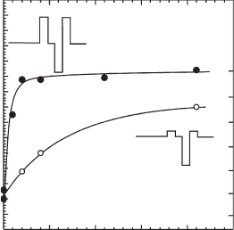
In [84] , we reported on a detailed study of the effect of barrier parameters on the properties of
strain engineered metamorphic QD nanostructures, with InAs QDs embedded in In
0.15
Al
0.85
As or
GaAs additional barriers set amid relaxed In
0.15
Ga
0.85
As CLs (insets in Fig. 16.10 ). As Al-containing
400
350
300
250
Activation energy of carrier
thermal escape (meV)
200
150
0510
GaAs barriers
In
0.15
AI
0.85
As barriers
LCL UCL
QD
LB
SL
UB
LCL
UCL
QD
LB
SL
UB
Upper and lower barrier thickness (ML)
15 20 25
Figure 16.10 Measured activation energy for thermal escape of carriers from QD structures with InAlAs and
GaAs barriers (closed and open circles, respectively) as a function of the barrier thickness. Insets show schematics of
the conduction band profi le for the structures, consisting of lower and upper InGaAs confi ning layers (LCL and UCL),
InGaAs spacer layers (SL), and lower and upper InAlAs or GaAs barriers (LB and UB). Lines are guides for the eye.
Reprinted from [84]. Copyright 2006, with permission from Elsevier.
CH016-I046325.indd 517CH016-I046325.indd 517 6/25/2008 3:16:24 PM6/25/2008 3:16:24 PM
518 Handbook of Self Assembled Semiconductor Nanostructures for Novel Devices in Photonics and Electronics
alloys cause a reduction of sizes of overgrown QDs [28] , a 4 ML thick In
0.15
Ga
0.85
As spacer layer
(SL) was grown atop of the InAlAs lower barrier, in order to not affect QD dimensions.
The additional barriers cause a relevant reduction of the PL quenching at high temperatures,
resulting in an increase of the PL intensity at RT (not shown here) by ⬃ 10 and ⬃ 500 (extrap-
olated values) when using 21 ML thick GaAs and In
0.15
Al
0.85
As barriers, respectively. In order
to have a more quantitative insight on the barrier effect, activation energies E
1
were derived for
structures with different barrier thicknesses, as plotted in Fig. 16.10 . It can be noticed how GaAs
barriers result in the increase of E
1
by about 100 meV, while the InAlAs ones cause a larger
increase. In this last case the PL quenching was so reduced that, for the structure with 21 ML
thick In
0.15
Al
0.85
As barriers, Eq. 16.6 could not be reliably fi tted to the experimental data, taken
only up to RT.
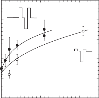
However, the use of higher barriers has the drawback of a blue shift of the QD emission wave-
length, as the carrier confi nement energies are also affected by the modifi ed band-structure. This
is shown in Fig. 16.11 where QD emission energy as measured by PL at 10 K is plotted as a func-
tion of the barrier thickness, for the same structures of Fig. 16.10 . The emission is blue shifted
as the barrier thickness increases: 21 ML thick InAlAs barriers result in a blue shift of ⬃ 8 0 m e V,
while GaAs counterparts cause a ⬃ 60 meV one. Some reports [32, 85, 86] indicate that the QD
emission energy presents an initial red shift and then a blue shift when increasing the thickness
of the InAlAs barrier. This effect has been interpreted as being due to In enrichment of QDs when
they are capped with InAlAs and reduced In segregation and intermixing [86] . However, other
works [87, 88] evidenced how the presence of an initial red shift depends on the growth tem-
perature of QDs, being absent for QDs grown at 480°C. As in our case QDs are grown at 460°C
[84] , we can conclude that intermixing and segregation effects are negligible and, therefore, only
the blue shift due to increased confi nement potential is present. Since it was observed from AFM
characterization [84] on structures of Figs 16.10 and 16.11 that QD sizes do not change when
adding InAlAs barriers (provided an InGaAs SL is grown before QD deposition), it can be con-
cluded that the blue shift of the QD emission is entirely related to the effectiveness of barriers in
increasing the confi nement of carriers.
LCL
UCL
QD
LB
SL
UB
LCL
UCL
QD
LB
SL
UB
1.140
1.22
1.24
1.26
1.28
1.30
1.20
1.32
GaAs barriers
In
0.15
AI
0.85
As barriers
1.120
1.100
1.080
Emission energy (eV)
Emission wavelength (μm)
1.060
1.040
1.020
1.000
0510
Upper and lower barrier thickness (ML)
15 20 25
Figure 16.11 Measured 10 K emission energy (left scale) and corresponding RT emission wavelength (right scale)
of QD structures with InAlAs and GaAs barriers (closed and open circles, respectively) as functions of the barrier
thickness. Insets show schematics of the conduction band profi le for such structures. Lines are guides for the eye.
Reprinted from [84]. Copyright 2006, with permission from Elsevier.
This detrimental effect of the enhanced barriers raises concerns about their usefulness in
structures aiming at long wavelength operation. However, the blue shift can be compensated for
by a suitable red shift determined by the intentional reduction of QD strain obtained by QD strain
engineering [84] .
Figure 16.12a provides an example, where a structure with a 190 nm thick In
x
Ga
1 ⫺
x
As LCL
( x ⫽ 0.31, f ⫽ 0.063), which should emit at RT at about 1.4 μ m, has an activation energy so
CH016-I046325.indd 518CH016-I046325.indd 518 6/25/2008 3:16:24 PM6/25/2008 3:16:24 PM