Marder M.P. Condensed Matter Physics
Подождите немного. Документ загружается.

21.
Optical Properties of
Semiconductors
21.1 Introduction
Chapter 19 made extensive use of the band theory of crystals to describe the trans-
port properties of semiconductors. It relied upon accurate values for energy gaps,
as well as upon effective masses of electrons and holes in the vicinities of band
maxima and minima. However, although the electrical properties of semiconduc-
tors depend crucially upon these quantities, the dependence is indirect. The most
accurate experimental determinations come from optical measurements, where pho-
tons drive electrons between various Bloch states. These measurements are not
nearly so simple as they sound. Apart from the difficulties of obtaining clean sur-
faces and pure samples, the process of optical absorption usually demands under-
standing some physics beyond the simple band theory. In the case of silicon and
germanium, the lowest-energy optical transitions are indirect, and they cannot pro-
ceed without aid from phonons. Even in the semiconductors with a direct optical
gap,
the absorption process is almost always complicated by excitons, excitations
resulting from the attraction between an electron and the hole it has left behind.
These observations confirm that no simple model such as the one-electron picture
of energy bands in a crystal will completely capture experimental phenomena in
solids and that the more precise experiments become, the more apparent will be
the discrepancies.
21.2 Cyclotron Resonance
In principle, once the band structure of the semiconductor is known, so are the ef-
fective masses, because they are nothing but second derivatives of the band energy
£ with respect to the Bloch wave vector k as in Eq. (16.28). This definition pro-
vides a way to find effective masses from band structure calculations, but is almost
useless if they are to be determined experimentally. Experimental determination
of effective masses requires a physical probe that tests dynamics directly, a service
provided in semiconductors by the technique of cyclotron resonance.
Effective masses enter into expressions for conductivity such as a = ne
2
r/m*,
but always in conjunction with the relaxation time, making it difficult to separate
the two. Cyclotron resonance solves this problem by introducing a magnetic field,
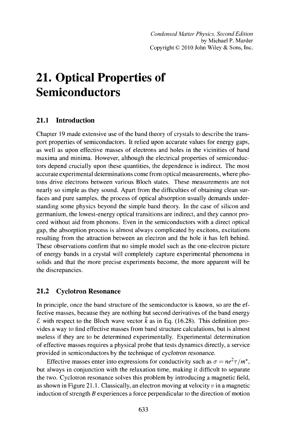
as shown in Figure
21.1.
Classically, an electron moving at velocity v in a magnetic
induction of strength B experiences a force perpendicular to the direction of motion
633
Condensed Matter
Physics,
Second Edition
by Michael P. Marder
Copyright © 2010 John Wiley & Sons, Inc.
634
Chapter
21.
Optical Properties of Semiconductors
Figure 21.1. Cyclotron resonance is pro-
duced in a semiconductor
by
applying a static
magnetic field and then applying microwave
radiation at the orbital frequency of the elec-
trons or holes.
of magnitude evB/c. Assuming it travels in a circular orbit of radius R and setting
the centripetal force equal to the magnetic force
m*v
2
evB „, ,
s
-=-
= (21-1)
R c
predicts an orbital frequency
V eB
ITA
m
\
B
1 ru /"11 ~>\
LÜ
C
=
—
= = 17.6 — —— GHz. (21.2)
R m*c m* [_kG_
Because this oscillation frequency is independent of the radius of the orbit, by
applying a perpendicular electric field with frequency
UJ
C
,
electrons can be excited
to large orbits and resonantly absorb incoming radiation. The relaxation time enters
nowhere in the resonance condition, although it plays a crucial role in determining
when the resonance is practically observable.
Calculation of Absorption. It is not too cumbersome to work out a detailed ex-
pression for the absorption of microwave radiation so long as the effective mass
m*
of an electron (or hole) can be taken to be a scalar. In the semiclassical approxima-
tion the dynamics of electrons are given by
j,
v eE e _, ->
y -\ = y x B.
T
is the relaxation time. (21.3)
r m* m*c
Taking the static B field to point along the z direction, and allowing both E and v
vary in time as
e~
luJt
,
one has that
/
IN eE
[-iLU + -)v = -
u!
c
(xvy
- yv
x
) (21.4)
1
É ( °
l
°\
^(-iLu + -)v = ~~-Lü
c
-1 0 0 \ v. (21.5)
r m
* \ 0 0 0/
Therefore
j = —nev = <TE, j is the current density, and n is the conduc- (21.6)
tion electron density.
Cyclotron Resonance 635
where
CTv
0"rv =
and
with
>xy
a
7
o
0
I
&xx ®xy
<7
= 1 —
Oxy
&xx
V
o o
cr
0
(l -iur)
(1
-ioJT)
2
+U)
2
T
2
CJQTÜJC
(1
-
ÎLOT)
2
+
L0
2
T
2
O-Q
1 — iiOT
'
2
ne r
0
0
c
z
m*
(21.7)
(21.8a)
(21.8b)
(21.8c)
(21.8d)
If the applied electric field is along x, then the time-averaged power absorbed by
the sample, (È
■
])/2, is proportional to the real part of o
xx
, which is
Re[o-J = a
0
-
LO}T
2
+
U>
2
T
2
+ 1
>
2
T
2
-LÜ
2
T
2
+\)
+Aüü
2
T
2
(21.9)
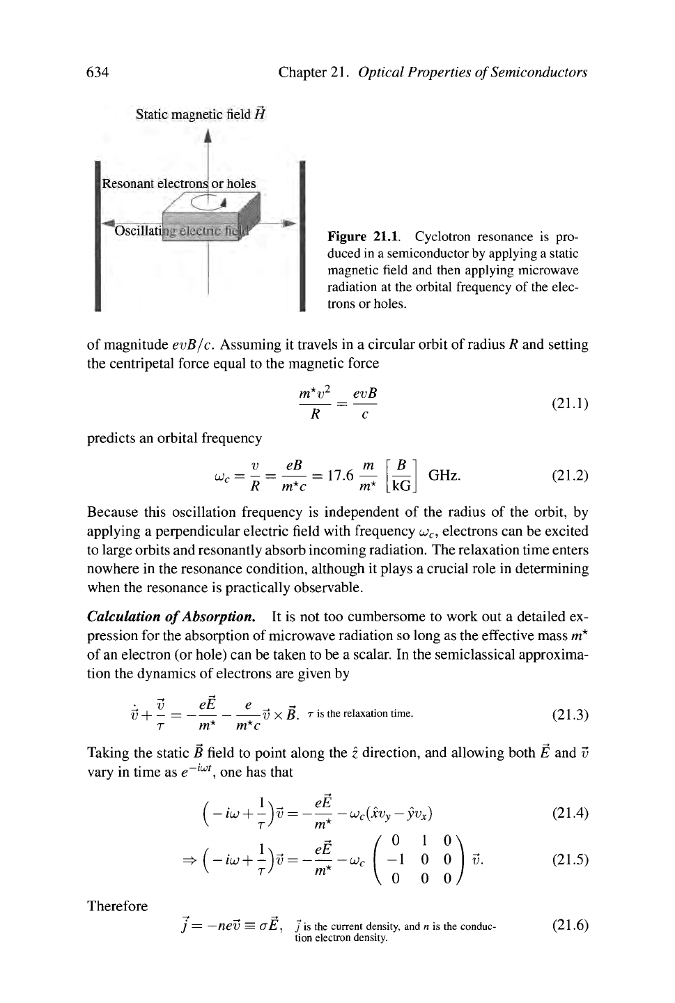
LÜ
A plot of Eq. (21.9) appears in Figure 21.2 for several values of
LOT.
G
3
n
o
X)
o
Figure 21.2. Plot of Eq. (21.9) for three val-
ues of
COT.
The frequency
ui
is the frequency
of the oscillating electric field E—in contrast
with
u>
c
,
which is the resonant frequency of
electrons governed by B. When
LÛT
<SC
1, col-
lisions damp the motion of
the
electron before
it has time to complete one cycle and absorb
much energy. No resonance is visible. By
the time
LOT
= 1 the relaxation time has be-
come large enough to permit observation of a
resonance. Varying
ui
c
is carried out by vary-
ing the strength of the static magnetic field,
while the oscillating electric field frequency
UJ
remains fixed.
LO
C
/LO
Practical Considerations. It was a substantial achievement by Dresselhaus et al.
(1953) and Lax et al. (1954) to turn cyclotron resonance into a practical tool, be-
cause for the experiment to work four competing requirements must be satisfied
simultaneously.
636 Chapter
21.
Optical Properties of Semiconductors
1.
One must guarantee that the semiclassical approximation be valid for the dy-
namics of the electrons or holes. This condition rules out optical frequencies
where
HOJ
>
1
eV and interband transitions become possible.
2.
The oscillating electric field must be able to penetrate the sample. This re-
quirement is equivalent to demanding that _ > „
p
, the plasma frequency of
Eq. (20.32). For undoped silicon and germanium at a temperature of
4
K, with
free carrier densities on the order of 10
13
cm
-3
, this condition can be satis-
fied, but already by a temperature of 70 K the carrier densities have risen high
enough that plasma oscillations mask the cyclotron resonance. This condition
rules out use of this technique in metals.
3.
The relaxation time must be long enough that _T > 1, according to Figure
21.2,
requiring (a) very pure samples to reduce impurity scattering and (b)
low temperatures to avoid phonon scattering.
4.
The free carrier density must be high enough that electrons and holes are avail-
able to absorb radiation. Although the density of free carriers is exponentially
small at low temperatures, this problem can be overcome by irradiating sam-
ples with photons at the energy of the band gap.
21.2.1 Electron Energy Surfaces
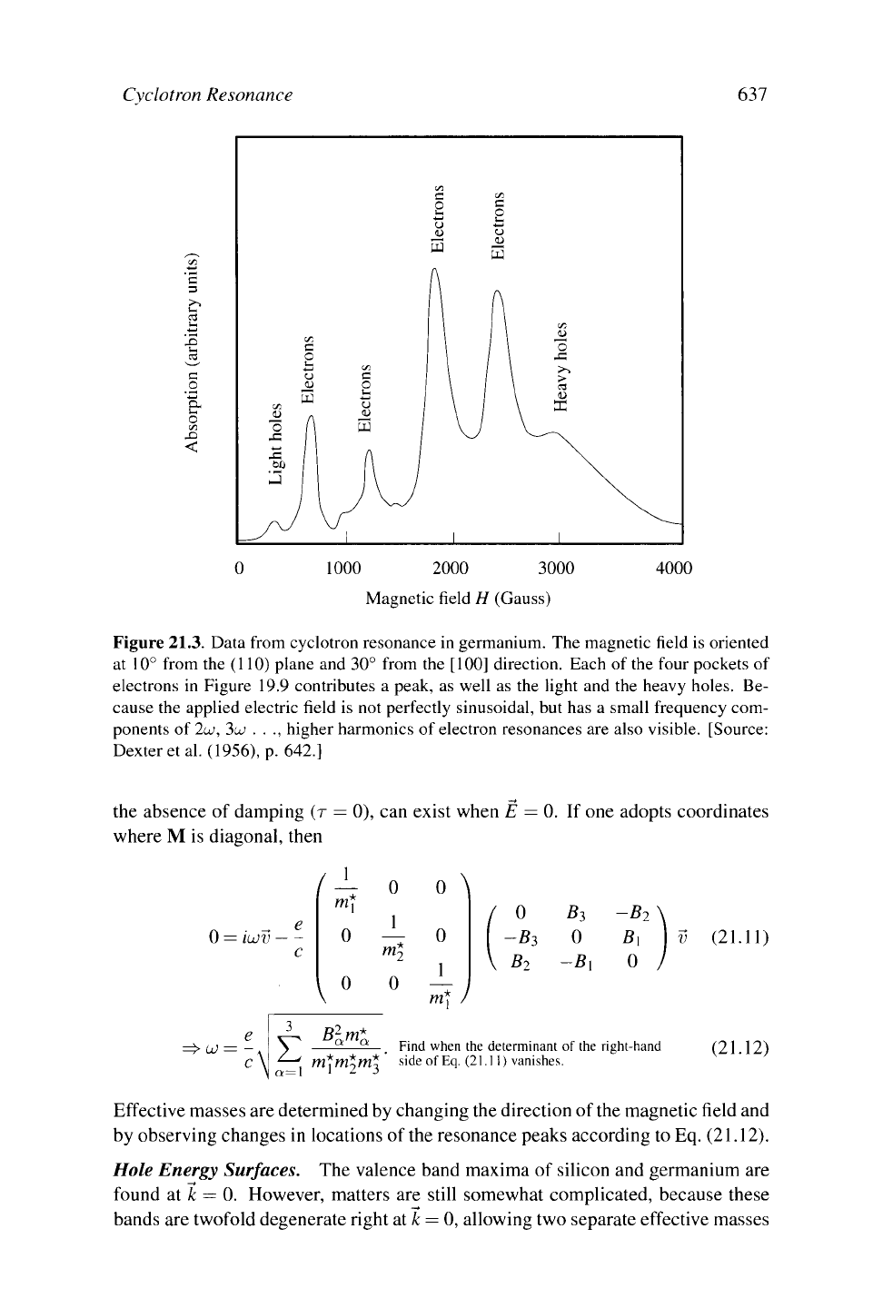
Data from a cyclotron resonance experiment in germanium appear in Figure 21.3.
There is a large number of peaks present. Because germanium is an indirect gap
semiconductor, its conduction band minimum does not lie atop k = 0, but instead
consists of four pockets of electrons straddling the zone boundaries in the (111)
direction: these electron pockets were shown in Figure 19.9(A). The constant en-
ergy surfaces in the neighborhood of the conduction band minima are not at all
spherical, but instead have the form
Every symmetric quadratic form can be diagonal-
ized; the energy is being expressed here in the ba- ,~,
-,
^
sis where the effective mass tensor is diagonal. In (_1.lUJ
the case of germanium, k\ is along (111), and for
silicon it is along (100).
where m\ = 1.64 m and m\ = m\ = 0.082 m. For arbitrary directions of the mag-
netic field, there is a separate peak from each pocket of electrons, although for
certain symmetry directions the peaks coalesce. For silicon, the situation is simi-
lar [Figure 19.9(B)], except that the conduction band minimum lies along the line
between 0 and (100), providing three rather than four distinct pockets of electrons.
The effective masses for silicon are m\ = 0.9 m and m\ = m\ = 0.19 m.
When the effective mass tensor is not diagonal, one must return to Eq. (21.4)
to see how the resonance condition changes. Rather than finding again the shape
of the absorption line, it is enough to ask for the frequencies at which resonances
occur. Resonances are located by searching for solutions of Eq. (21.4) which, in
£ = —
2
L/ft
7,2 ul ul
_LJ._2._L_1
mî
mï-i
Cyclotron Resonance 637
c
3
C3
G
O
<
1000 2000 3000
Magnetic field H (Gauss)
4000
Figure 21.3. Data from cyclotron resonance in germanium. The magnetic field is oriented
at 10° from the (110) plane and 30° from the [100] direction. Each of the four pockets of
electrons in Figure 19.9 contributes a peak, as well as the light and the heavy holes. Be-
cause the applied electric field is not perfectly sinusoidal, but has a small frequency com-
ponents of
2LÜ,
2>iü
. . ., higher harmonics of electron resonances are also visible. [Source:
Dexter et al. (1956), p. 642.]
the absence of damping (r = 0), can exist when Ê = 0. If one adopts coordinates
where M is diagonal, then
/
e
: iüJV
c
1
m*
0
0
0
1
0 \
0
1
(21.11)
to
i
a=l
B
2
m*
m\m\m\
Find when the determinant of the right-hand
side of Eq. (21.11) vanishes.
(21.12)
Effective masses are determined by changing the direction of the magnetic field and
by observing changes in locations of the resonance peaks according to Eq. (21.12).
Hole Energy Surfaces. The valence band maxima of silicon and germanium are
found at k — 0. However, matters are still somewhat complicated, because these
bands are twofold degenerate right at k = 0, allowing two separate effective masses
638 Chapter
21.
Optical Properties of Semiconductors
for holes. The heavy hole in germanium has
m*
H
« 0.28 m and the light hole has
m\
« 0.044 m, while the corresponding numbers for silicon are m^ ss 0.49 m and
m*
L
~ 0.16 m.
21.3 Semiconductor Band Gaps
21.3.1 Direct Transitions
Direct gap semiconductors, as defined in Section
19.3.1,
have a maximum of the
valence band sitting directly below the minimum energy state of the conduction
band in k space.
The theory for optical transitions in this case starts with Eq. (20.70), which
shows a contribution to absorption whenever the energy
hco
of an incoming photon
equals the difference £„/
—
£„ between two energy states. In order to place the
theoretical result in the most convenient form, it is helpful to recall Eq. (20.14) and
rewrite (20.70) as
ImM = ^ ^(/
/
-/
/
0(/|4|/
,
)(/
/
|
J
P/3|0^(£/'-£/-M (21.13)
m
UJ
V
w
f2ire\
2
1
-^
= vT, (kni\P
a
\kn
2
){kn
2
\P
ß
\kn
l
)6(8,
n2l
-8,
nii
-nLv) (21.14)
kn\U2
Labeling the states now by Bloch index k and band indices n\ and «2- The Bloch indices
k of the initial and final states must be the same or else the matrix element vanishes. The
sum is understood to include only cases where n\k is occupied, and
n-^k
is unoccupied.
= (—) |P
a/3
M|
2
Z>j(fia;), (21-15)
\
moj
/
where
lp ,
M2_
£W (fallfato^nzlPgl^iQ^g g-£ g-«a;)
1 Q/SMI =
E tS(S- r-£ r-hui)
(2L16)
*—'n\n2k
v
nik n\k >
and
H^)
= \ E/(
£
^-^-M- (21.17)
n\nik
The absorption has been expressed as a product of an average matrix element
\P\ and the joint density of
states
D
y
The reason to place the expression in this
form is that the averaged matrix element has no particular reason to exhibit sharp
changes as a function of frequency and can often be approximated as a constant, but
the joint density of states D
}
is extremely sensitive to details of the band structure
and depends strongly upon frequency. The joint density of states carries all the
information about whether there exist pairs of occupied and unoccupied states with
the right energy separation so that the photon can excite an electron between them.
It vanishes when this condition is not met. In addition, whenever the band energies
Z
n
£
and Z
n
-
k
run parallel to one another as a function of k, Dj exhibits van Hove
singularities, as defined in Section 7.2.5.
Semiconductor Band Gaps
639
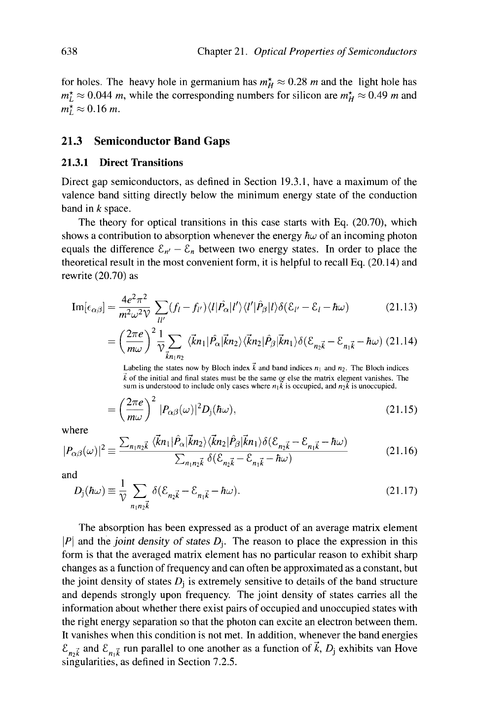
For direct band gap semiconductors to which Eq. (21.14) applies, one must
turn to alloys, such as GaAs, or InSb. It is natural to expect that right at the
threshhold of absorption, where hu > £
g
, the matrix element \P
a
ß\ has no reason
to vary rapidly, so optical absorption should be proportional to the joint density of
states Dj(hu). Because both valence and conduction bands have parabolic extrema
around k = 0,
8.
c
(k)
—
£
v
(k)
—
£
g
is a parabolic function vanishing at k
—
0, and Dj
must therefore exhibit the van Hove singularity discussed in Section 7.2.5; that is,
Dj should vanish for hu < £
g
, and then should rise as ^hu
—
S.
g
.
There are few cases where such behavior is actually observed. One of them ap-
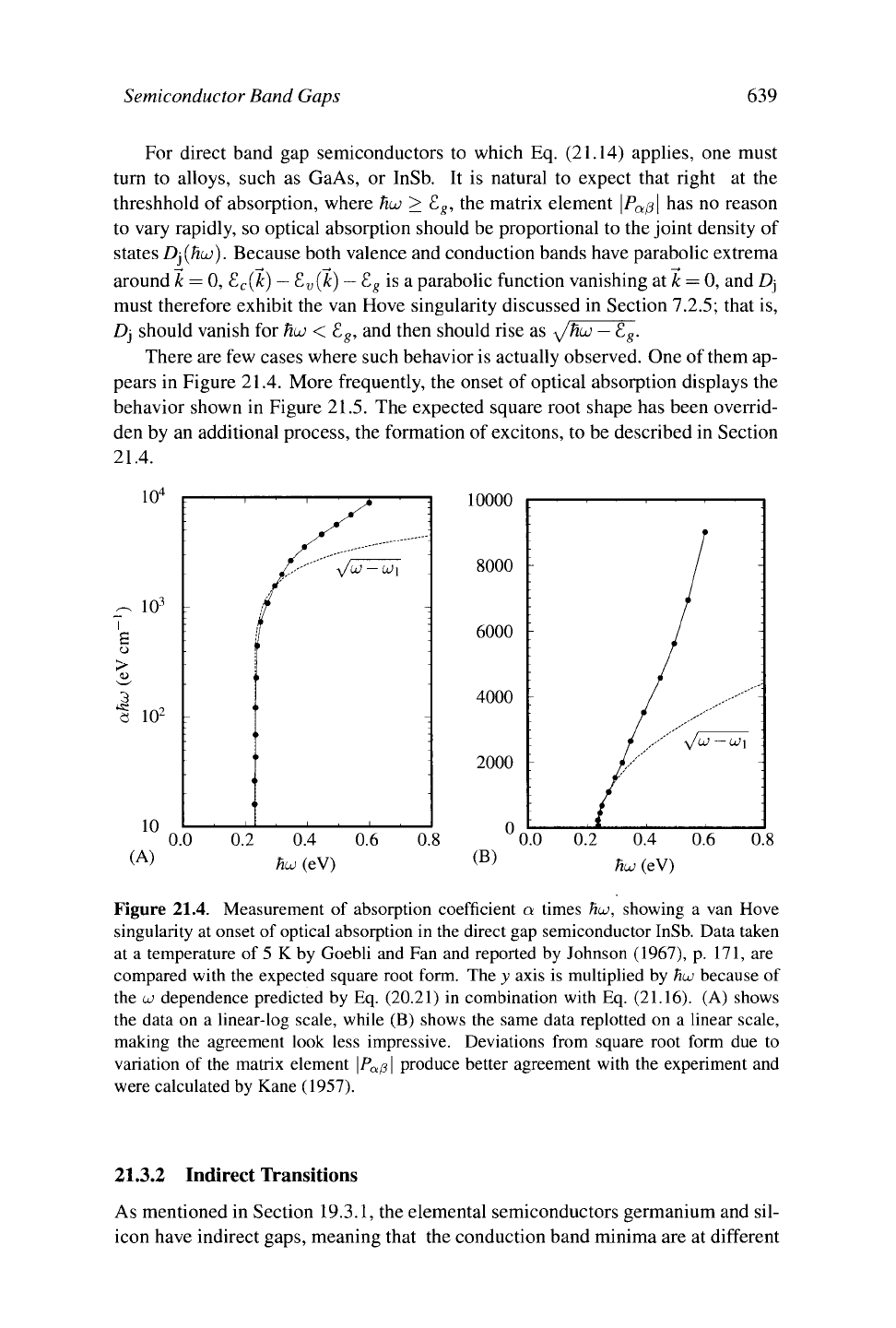
pears in Figure 21.4. More frequently, the onset of optical absorption displays the
behavior shown in Figure 21.5. The expected square root shape has been overrid-
den by an additional process, the formation of excitons, to be described in Section
21.4.
10
4
10
3
r
I
10
2
10
(A)
;
.
'
/,.--"
yju -
i
i
;
~U\
10000
8000
6000
4000 -
2000
L
0.0 0.2
0.4
hu (eV)
0.6
0.8
(B)
0.2 0.4 0.6
hu (eV)
0.8
Figure 21.4. Measurement of absorption coefficient a times hu, showing a van Hove
singularity at onset of optical absorption in the direct gap semiconductor InSb. Data taken
at a temperature of 5 K by Goebli and Fan and reported by Johnson (1967), p. 171, are
compared with the expected square root form. The y axis is multiplied by hu because of
the u dependence predicted by Eq. (20.21) in combination with Eq. (21.16). (A) shows
the data on a linear-log scale, while (B) shows the same data replotted on a linear scale,
making the agreement look less impressive. Deviations from square root form due to
variation of the matrix element \P
a
ß\ produce better agreement with the experiment and
were calculated by Kane (1957).
21.3.2 Indirect Transitions
As mentioned in Section
19.3.1,
the elemental semiconductors germanium and sil-
icon have indirect gaps, meaning that the conduction band minima are at different
640 Chapter
21.
Optical Properties of Semiconductors
1
1.50 1.52 1.54 1.56
HLJ
(eV)
Figure
21.5.
Measurement of absorption coefficient a in gallium arsenide, showing mod-
ification of absorption due to excitons. [Source: Sturge (1962),
p.
771.]
locations in k space from the valence band maxima. It is possible for light to excite
electrons between the valence band maximum and conduction band minimum, but
only with the assistance of phonons so as to permit conservation of momentum.
The microscopic theory of such transitions is therefore rather involved. The initial
and final states of the system differ not only because an electron has moved to a
new state, but also because the number of phonons has changed. The interaction
Hamiltonian between photons and solid does not include a term for phonons, so
any matrix element with the interaction Hamiltonian in the middle and with such
initial and final states on either side must vanish. These transitions show up only
at second order in perturbation theory. Fortunately, it is possible to guess the form
of the final result without going through detailed calculations, using only conser-
vation laws. In order for the Bloch index of an electron to change by 5k, either a
phonon of wave vector — 5k and energy
hu)
p
u(5k)
must be created, or a phonon of
wave vector 5k and energy hw^ôk) must be destroyed, in order to conserve crystal
momentum. In order for energy to be conserved, one must have
HLÜ
= £
c
— £
v
±
HiOph
(5k).
E-c
is the energy of an electron in the conduc- (21.18)
tion band, and £„ is the energy of an electron
in the valence band.
At temperatures much lower than the Debye temperature, there will be very few
phonons residing naturally in the sample, and the negative term in Eq. (21.18)
where a phonon is destroyed should cease to provide transitions. So according
to Eq. (21.18), optical absorption in silicon and germanium should appear in two
stages, at a first and a second frequency, with the strength of the absorption at the
first frequency diminishing steadily with temperature.
The shape of the absorption curve can similarly be estimated. A complete for-
mula will have to involve various matrix elements, sums over intermediate states,
1.1
| 0.9
o
a
0.7
o s
Excitons
641
and so on. Assuming that the energy dependence of all these can be neglected, the
extinction coefficient
K
should be proportional to
KOC^J (e.
c
(k
c
)-£,
v
(k
v
)-hL;±hLü
ph
(Sk)) (21.19)
k(k
v
= J d£
c
J d£
v
D
c
(£.
c
)D
v
(E.
v
)6 {£.
c
-E.
v
-hüj±hu&) (21.20)
Neglect
the Sk dependence of w
p
h.
oc / dS.
c
/ d£.
v
JS.
C
—
£.
g
\/—8-
v
S (£
c
—
E
v
—
hu;±hujph) (21.21)
"S
Letting
£
g
be the band gap, setting the valence band maximum to
zero,
and using the generic three-dimensional forms of the density
of
states near a band maximum or minimum.
■hw^hiüpb
d£
c
y£
c
-£
g1
y/iu;-£
c
=F/kjp
n
(21.22)
= (/^T^
ph
-£
g
)
2
f
dy^^Y^.
(21.23)
Jo
Letting
y = (E
c
- £
s
)/(fiw
=F
f>u}
ph
- £
g
). From Eq.
(21.22),
the
result
vanishes, however, unless
HUJ
> £
g
^fHw
p
h.
The value of the
integral
is not important, just the fact that it is constant.
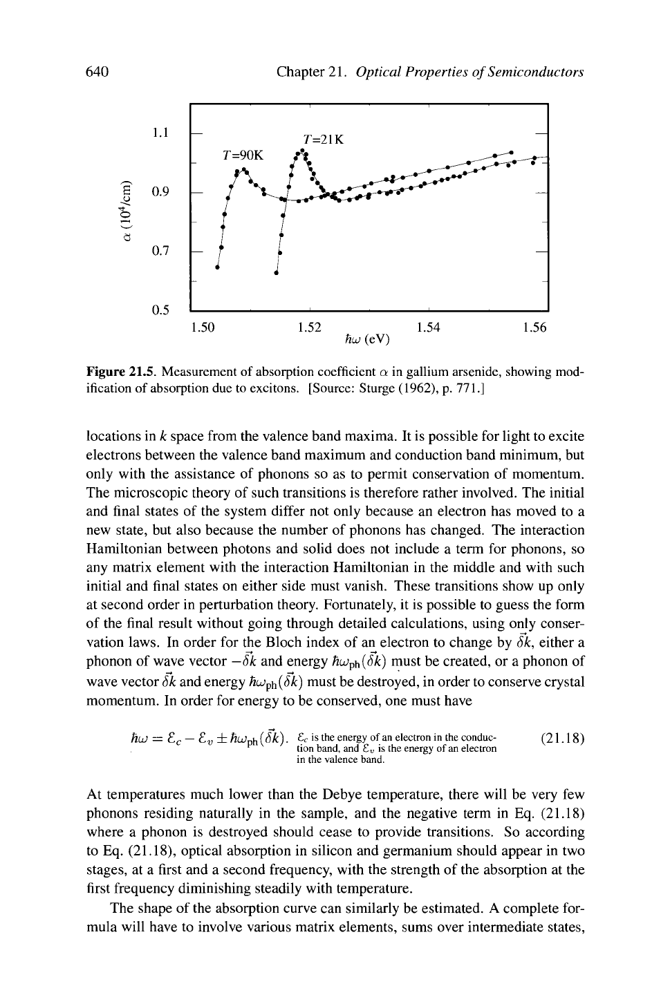
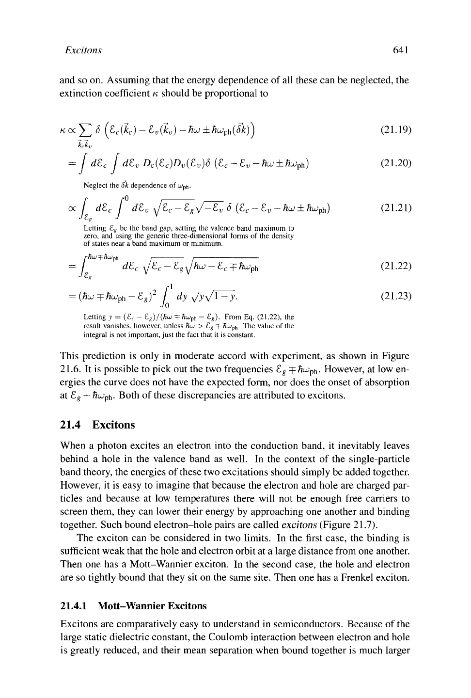
This prediction is only in moderate accord with experiment, as shown in Figure
21.6.
It is possible to pick out the two frequencies £
s
^hio
P
h. However, at low en-
ergies the curve does not have the expected form, nor does the onset of absorption
at £
g
+
hiü
p
h.
Both of these discrepancies are attributed to excitons.
21.4 Excitons
When a photon excites an electron into the conduction band, it inevitably leaves
behind a hole in the valence band as well. In the context of the single-particle
band theory, the energies of these two excitations should simply be added together.
However, it is easy to imagine that because the electron and hole are charged par-
ticles and because at low temperatures there will not be enough free carriers to
screen them, they can lower their energy by approaching one another and binding
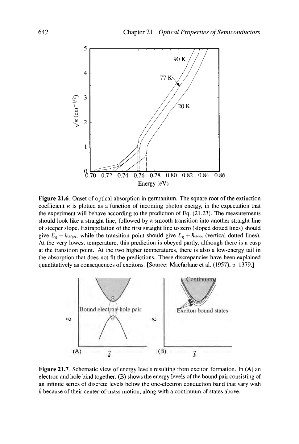
together. Such bound electron-hole pairs are called excitons (Figure 21.7).
The exciton can be considered in two limits. In the first case, the binding is
sufficient weak that the hole and electron orbit at a large distance from one another.
Then one has a Mott-Wannier exciton. In the second case, the hole and electron
are so tightly bound that they sit on the same site. Then one has a Frenkel exciton.
21.4.1 Mott-Wannier Excitons
Excitons are comparatively easy to understand in semiconductors. Because of the
large static dielectric constant, the Coulomb interaction between electron and hole
is greatly reduced, and their mean separation when bound together is much larger
642 Chapter
21.
Optical Properties of Semiconductors
0.70 0.72 0.74 0.76 0.78 0.80 0.82 0.84
Energy (eV)
0.86
Figure 21.6. Onset of optical absorption in germanium. The square root of the extinction
coefficient K is plotted as a function of incoming photon energy, in the expectation that
the experiment will behave according to the prediction of Eq. (21.23). The measurements
should look like a straight line, followed by a smooth transition into another straight line
of steeper slope. Extrapolation of the first straight line to zero (sloped dotted lines) should
give E
g
—
Awph,
while the transition point should give E
g
+
hiü
p
h
(vertical dotted lines).
At the very lowest temperature, this prediction is obeyed partly, although there is a cusp
at the transition point. At the two higher temperatures, there is also a low-energy tail in
the absorption that does not fit the predictions. These discrepancies have been explained
quantitatively as consequences of
excitons.
[Source: Macfarlane et al. (1957), p. 1379.]
Figure 21.7. Schematic view of energy levels resulting from exciton formation. In (A) an
electron and hole bind together. (B) shows the energy levels of the bound pair consisting of
an infinite series of discrete levels below the one-electron conduction band that vary with
k because of their center-of-mass motion, along with a continuum of states above.