Middleton W.M. (ed.) Reference Data for Engineers: Radio, Electronics, Computer and Communications
Подождите немного. Документ загружается.

20-1 00
contaminants or cause native oxides
to
form
on
sili-
con. This subsection will be divided into subsubsec-
tions discussing groupings of process steps that could
be adapted
to
device fabrication in cluster tools.
SWP
techniques can be usefully applied to CMOS,
bipolar, or any BiCMOS-like combination. The appli-
cation
to
CMOS device processing will be discussed
here as an example of the application of
SWP. The
interrelationship between CMOS device design param-
eters and
SWP with in situ process control will be dis-
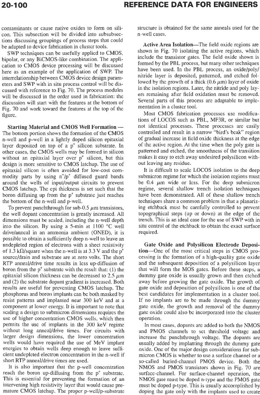
cussed with reference to Fig.
70.
The process modules
will be discussed in the order used in fabrication: the
discussion will start with the features at the bottom of
Fig.
70
and work toward the features at the top of the
figure.
Starting Material and CMOS Well Formation
-
The bottom portion shows the formation of the CMOS
n-well and p-well in a lightly doped silicon epitaxial
layer deposited
on
top of a p+ silicon substrate.
In
other cases, the CMOS wells may be formed in silicon
without an epitaxial layer over p+ silicon, but this
design is more sensitive to CMOS latchup. The use of
epitaxial silicon is often avoided for low-cost com-
modity parts by using n+/p' diffused guard bands
around the wells of input/output circuits to prevent
CMOS latchup. The epi thickness is set such that the
boron diffusing up from the p+ substrate just reaches
the bottom of the n-well and p-well.
To prevent punchthrough for sub-0.5 pm transistors,
the well dopant concentration is greatly increased. All
dimensions must be scaled, including the n-well depth
into the silicon. By using a
5-min
at
1100
"C well
drive/anneal in an ammonia ambient
(ONED),
it is
possible to obtain a sufficiently deep n-well to leave an
undepleted region of electrons with a sheet resistivity
of 1.3 kWsquare when the n-well is at 3.3 V and the p"
source/drain and substrate are at zero volts. The short
RTP anneal/drive time results in less up-diffusion of
boron from the p+ substrate with the result that:
(1)
the
epitaxial silicon thickness can be decreased to
2.5 pm
and
(2)
the substrate dopant gradient is increased. Both
results are useful for preventing CMOS latchup. The
phosphorus and boron implants can be both masked by
resist patterns and implanted near 300 keV and at a
component at lower energy. It is important to note that
scaling a design to submicron dimensions requires the
use of higher concentration CMOS wells, which then
permits the use of implants in the 300 keV regime
without long anneal/drive times. For circuits with
larger design dimensions, the lower concentration
wells would have required the use of MeV implant
energies
to
obtain wells deep enough to leave suffi-
cient undepleted electron concentration in the n-well if
short RTP annealfdrive times are used.
It is also important that the p-well concentration
reach the boron up-diffusing from the p' substrate.
This is essential for preventing the formation of an
intervening high resistivity layer that would cause pre-
mature CMOS latchup. The proper p-well/p-substrate
structure is obtained for the same anneals used for the
n-well cases.
Active Area Isolation-The field oxide regions are
shown
in
Fig.
70
isolating the active regions, which
include the transistor gates. The field oxide shown is
formed by the PBL process, but many other techniques
have been used.
In
the PBL process, an oxide/poly/
nitride layer is deposited, patterned, and etched fol-
lowed by the growth of a thick
(0.6
pm) layer of oxide
in the isolation regions. Later, the nitride and poly lay-
ers remaining after field oxidation must be removed.
Several parts of this process are adaptable
to imple-
mentation in a cluster tool.
Most CMOS fabrication processes use modifica-
tions of LOCOS such as PBL, MFSR, or similar but
not identical processes. These processes are easily
controlled and result in a narrow "bird's beak" region
of gradual increase in field oxide thickness at the edge
of the active region. At the time when the poly gate
is
patterned and etched, the smoothness of the transition
makes
it
easy to etch away undesired polysilicon with-
out leaving any residue.
It is difficult to scale LOCOS isolation to the deep
submicron regime for which the isolation regions must
be
0.4
pm wide or less. For the deep submicron
regime, several shallow trench isolation techniques
have been demonstrated. All of these shallow trench
techniques share a common problem
in
that a planariz-
ing etchback must be carefully controlled to prevent
topographical steps (up or down) at the edge
of
the
trench. This is an ideal case for the use of
SWP
with in
situ control of the etchback to obtain the exact surface
required.
Gate Oxide and Polysilicon Electrode Deposi-
tion-One of the most critical steps in CMOS pro-
cessing is the formation of a high-quality gate oxide
and the subsequent deposition of a polysilicon layer
that will form the MOS gates. Before these steps, a
dummy gate oxide is usually grown and then etched
away before growing the gate oxide. The growth of
gate oxide and deposition of polysilicon is one of the
best candidates for implementation in a cluster tool.
If no implants are to be made through the dummy
gate oxide, the growth and removal of the dummy
gate oxide could also be incorporated into the cluster
operation.
In most cases, dopants
are
added to both the
NMOS
and PMOS channels to set threshold voltage and
increase the punchthrough voltage. The dopants are
usually added by implanting through the dummy gate
oxide. One of the major design considerations for sub-
micron CMOS is whether to use a surface channel or a
so-called buried-channel PMOS device. Both the
NMOS and PMOS transistors shown in Fig.
70
are
surface-channel. For surface-channel operation, the
NMOS
gate must be doped n-type and the PMOS gate
must be doped p-type. This is usually accomplished by
doping the gate only with the implants used to create
20-1
01
the NMOS and PMOS source/drains. For a PMOS
“buried-channel” transistor, the polysilicon is doped
n-
type for both the
NMOS
and PMOS transistors. For
buried-channel, a boron implant must be made into the
surface of the silicon. This creates a pn junction imme-
diately underneath the gate oxide. For a properly
designed transistor, the boron implant is shallow
enough that the p-type region is completely depleted
by the built-in voltage of the pn junction. This depleted
region makes it easier for the drain voltage to reduce
the potential barrier at the source with resultant excess
subthreshold leakage for very-short-channel PMOS
transistors. For very-short-channel PMOS devices, the
surface-channel device is the best choice because the
depletion layer
is
much thinner for surface-channel
than for buried-channel.
It is especially important to grow the gate oxide at a
low temperature when a buried-channel PMOS device
is fabricated by using a boron implant through the
dummy gate oxide. If the oxidation temperature is too
high, boron diffusion will make it difficult to keep the
boron profile shallow. This is especially true for transis-
tors designed for the deep submicron where the pn
junction may need
to
be
0.05
pm deep or less. Surface-
channel PMOS design seems better adapted to RTP in
dry
oxygen ambient at high temperatures.
In
this case,
the boron is implanted into the poly after the growth of
the oxide
so
boron diffusion does
not
limit the choice
of
RTP
parameters for gate oxidation. Boron diffusion
through oxide
is
enhanced by the presence of hydrogen
or fluorine, and this must be considered in the design of
the subsequent process steps.
Gate Structure Formation-Following the deposi-
tion of polysilicon, the gate is patterned and etched.
Later, one or two layers of oxide will be deposited and
etched anisotropically to form sidewall spacers at the
side of the gate as shown for the
NMOS
gate and
PMOS
gate in Fig.
70.
As stated earlier, the control of
poly linewidth is the most critical parameter in CMOS
fabrication.
SWP
with multiple sensors for etchant
species and temperature will be required
to
obtain suf-
ficient control of linewidth to build transistors with
0.35
pm linewidths and below. It is also extremely
important that the etch removes all polysilicon from
regions not covered by resist during the etch: sensors
are needed to determine when the poly has been
removed from all regions, including topography step
regions where the poly will be thicker after conformal
deposition.
In
some cases, the sidewall oxide spacer may be
formed by thermal oxidation rather than by deposition.
In
most cases, implants of light or medium dose may
be made before the deposition
of
one of the sidewall
oxide spacers. These so-called LDD or lightly doped
drain implants must go under the edge
of
the gate by
lateral straggle at implant or later diffusion. Also of
major importance is that the LDD junction be as shal-
low as possible to decrease the ability of the drain volt-
age
to
influence the source potential barrier.
As a final step, a pad oxide will be deposited before
the implants of the next module. This pad oxide pro-
tects the silicon from contaminants in the photoresist
process, randomizes the source/drain implants to mini-
mize channeling, and protects the silicon during
anneal of the source/drain implants.
Source/Drain Junctions with or without Sili-
cide-Relatively high-dose arsenic and/or phosphorus
implants must be made for the
NMOS
source/drains
and a boron implant for the PMOS source/drains.
These implants go through the pad oxide and must be
blocked by the field oxide, poly gates, and sidewall
oxide spacers adjacent to the gates
so
that the source/
drains
are formed
only
in the active areas not covered by
gate. A particular design concern for surface-channel
CMOS is that the poly must be thin enough that the
source/drain dopants reach the bottom surface of the
poly (after anneal).
Rapid thermal anneal of the
source/drain implants is an obvious choice for
SWP.
This is particularly important when the junctions must
be kept shallow.
Many CMOS processes include the formation of
silicide over the active regions and the polysilicon
gates. After anneal of the source/drain implants, an
additional oxide may be deposited and anisotropically
etched to increase the width of the
sidewall oxide
spacer before silicide processing (see Fig.
70)
and
leave the polysilicon and active areas free of oxide.
In
the “salicide” direct react process, titanium metal is
deposited; layered titanium nitride/titanium silicide is
formed by reacting in a nitrogen ambient; the titanium
nitride is etched away leaving silicide over exposed sil-
icon and polysilicon; and finally the remaining silicide
is
annealed at a slightly higher temperature to obtain
the lowest possible sheet resistivity from the TiSi,
compound. Precise control of titanium thickness,
ambient pressures, and react/anneal temperatures is
required for this silicide process, making this process
an obvious choice implementation with a cluster tool.
It
should be noted that the formation of a silicide
over the source/drain junctions requires that these
junctions be deep enough to prevent shorting by the
silicide. Usually when silicide is used,
it
is not desir-
able to have very shallow junctions for source/drain;
the shallow junction for the CMOS transistors is
obtained by the
LDD
structure formed earlier in the
process.
Metallization and Interlevel Isolation-Fig.
70
shows a schematic representation
of
the formation of
two levels of metal interconnect separated by interlevel
insulators. The first metal may use tungsten plugs in
the vias with copper-doped aluminum as the top inter-
connect level. The use of other combinations of metals
is being investigated. The interlevel insulators will be
combinations of deposited undoped and doped oxides.
In some processes, a layer of oxide doped with phos-
phorus and/or boron will be reflowed at a moderate
temperature to smooth the insulator surface before
20-1
02
subsequent deposition of a metal layer. Phosphoms-
doped oxides also play an important role in preventing
contamination to the gate oxide by mobile ions.
In
other cases, a resist coat or spin-on glass followed by
etchback planarization will be used. Etchback pla-
narization processes in general require very accurate
measurement of oxide thicknesses and feedback con-
trol on etch duration.
One of the most critical problems that can be
addressed by
SWP
with sensors for feedback control is
etch of contact and via. For devices designed for deep
submicron dimensions, the height-to-width aspect
ratio can be in the range of
2-3.
This can be a special
problem for contacts from metal-1 because the aspect
ratio will be different for contacts to active area and to
poly over field oxide (see Fig.
70). Vias always con-
nect metal-1 and metal-2,
so the height-diameter ratio
should be the same for all vias.
If
silicide is used to clad the active areas, it is
extremely important
to limit the temperatures used in
the metal/interlevel oxide processes. The problem is
that the dopants in the source/drains will diffuse into
the silicide. The problem is especially severe for
PMOS, in which case it is best to keep these later tem-
peratures
700
“C or lower. In some applications, tem-
peratures as high as
800
“C can be used.
Gate oxide is subject to damage during processing
steps after poly gate etch.
Dry etching of oxides and
metals using high-energy ions can cause radiation dam-
age
to
the gate oxide. Mechanical stress from subse-
quent layers can influence the effect of radiation damage
on
the gate oxide. The effect of damage to the gate oxide
is most noticeable for
NMOS
transistors and can affect
the resistance of the
NMOS transistor to hot carrier
stress. It is well known that hydrogen will weakly bond
to the damage centers and also make it easier to create
additional damage centers. Hydrogen can also accelerate
boron diffusion through gate oxide if the temperatures
are
too high.
In
principle, it is desired to minimize the
use
of
hydrogen ambient during later processing, but this
is
difficult to accomplish. It is important to limit process-
ing temperatures
if
an ambient with considerable hydro-
gen partial pressures is used.
All
of the above parameters
should be monitored during
SWP.
Protective Overcoat Layer-The final step after
etch of the last metal interconnect is to place a protec-
tive layer over the metal and remove the protective
overcoat over the bond pads.
SILICON-ON-INSULATOR
TECHNOLOGY AND DEVICES*
Silicon-on-insulator (SOI) technology is a primary
candidate
to
provide the improved performance,
cheaper processing, and unique device structures
required for future generations of
ICs.?
Development
*
This section
was
contributed
by
H.
H.
Hosack.
of this technology has been significantly enhanced by
the fact that in addition to improved performance and
yield, devices fabricated
on
SO1 substrates exhibit sig-
nificantly increased tolerance to transient radiation and
single event upset
(SEU).$
This radiation tolerance has
resulted in considerable interest in SO1 technology
development for devices useful to both space science
missions and military electronics.
SO1
Material
Options
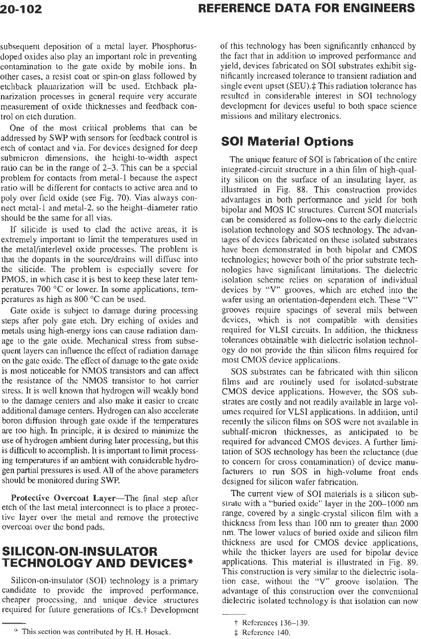
The unique feature of SO1 is fabrication of the entire
integrated-circuit structure in a thin film of high-qual-
ity silicon
on
the surface of an insulating layer, as
illustrated in Fig.
88. This construction provides
advantages in both performance and yield for both
bipolar and MOS IC structures. Current SO1 materials
can be considered as follow-ons to the early dielectric
isolation technology and
SOS technology. The advan-
tages of devices fabricated
on
these isolated substrates
have been demonstrated
in
both bipolar and CMOS
technologies; however both of the prior substrate tech-
nologies have significant limitations. The dielectric
isolation scheme relies
on
separation of individual
devices by
“V”
grooves, which are etched into the
wafer using an orientation-dependent etch. These
“V”
grooves require spacings of several mils between
devices, which is not compatible with densities
required for VLSI circuits. In addition, the thickness
tolerances obtainable with dielectric isolation technol-
ogy do not provide the thin silicon films required for
most CMOS device applications.
SOS
substrates can be fabricated with thin silicon
films and are routinely used for isolated-substrate
CMOS device applications. However, the
SOS
sub-
strates are costly and
not
readily available in large vol-
umes required for VLSI applications.
In
addition, until
recently the silicon films
on
SOS
were
not
available in
subhalf-micron thicknesses, as anticipated to be
required for advanced
CMOS
devices.
A
further limi-
tation of
SOS
technology has been the reluctance (due
to concern for cross contamination) of device manu-
facturers to
run
SOS
in high-volume front ends
designed for silicon wafer fabrication.
The current view of
SO1
materials is a silicon sub-
strate with a “buried
oxide”
layer in the
200-1000
nm
range, covered by a single-crystal silicon film with a
thickness from less than
100
nm
to greater than
2000
nm. The lower values of buried oxide and silicon film
thickness are used for CMOS device applications,
while the thicker layers are used for bipolar device
applications. This material is illustrated in Fig.
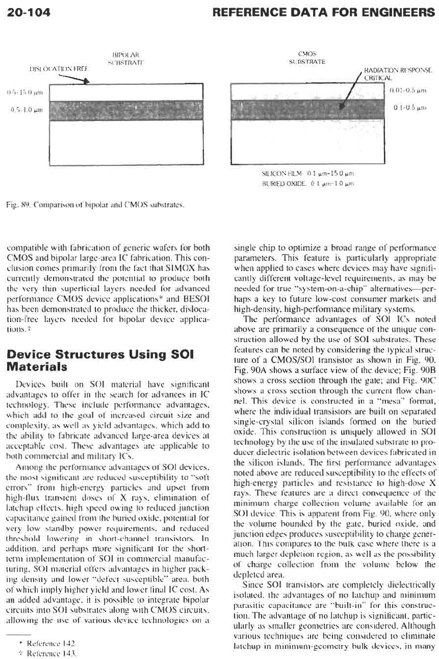
89.
This construction is very similar to the dielectric isola-
tion case, without the
“V” groove isolation. The
advantage of this construction over the conventional
dielectric isolated technology
is
that isolation can now
t
References
136-139
$
Reference
140.
INTEGRATED CIRCUITS
20-1
03
n-WELL
U
....
(A)
Bulk
CMOS
daulce.
P
(BJ Slllcon-on-Insulator
deulce
Fig.
88.
Silicon-on-insulator device structure.
be provided by simply etching the silicon layer to form
“moats” around isolated silicon islands, which can be
accomplished at geometries as narrow as allowed by
lithographic tools. The advantage of the current
SO1
materials over
SOS
is that the all-silicon construction
ensures compatibility with large volume front ends
designed specifically for silicon technologies, as well
as allowing potential availability from commercial sili-
con wafer manufacturers.
Several alternative constructions have been pro-
posed and investigated for producing SO1 materials.*
Among these are Separation by IMplantation of
OXy-
gen
(SIMOX),
Bond and Etchback
(BESOI),
Zone
Melt Recrystallization
(ZMR),
Field Isolation by
Porous Oxidation of Silicon
(FIPOS),
and Epitaxial
Lateral Overgrowth (ELO). Each of these techniques
has its own specific advantages and disadvantages, but
thus far only
two,
SIMOX and BESOT, have shown
the potential for being manufacturable technologies
*
Reference
141,
20-1
04
REFERENCE
DATA
FOR
ENGINEERS
BIPOLAR
SLJBSTRATE
DISLOCATION
FREE
CMOS
SUBSTRATE
RADlATlON RESPONSE
/
CRITICAL
I
0.01-0.5
km
0.515.0
pm
SILICON
LlLM:
0.1 pm-15.0
pm
BURIEDOXIDE:
0.1 km1.0
pm
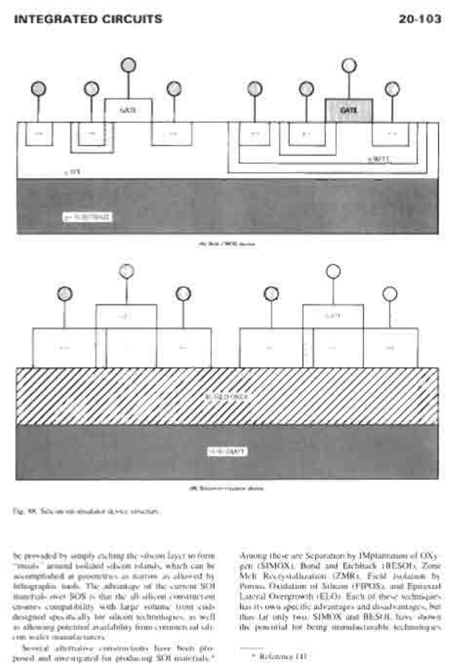
Fig. 89.
Comparison of bipolar
and
CMOS substrates.
compatible with fabrication of generic wafers for both
CMOS
and bipolar large-area
IC
fabrication. This con-
clusion comes primarily from the fact that
SIMOX
has
currently demonstrated the potential to produce both
the very thin superficial layers needed for advanced
performance
CMOS
device applications* and
BESOI
has been demonstrated to produce the thicker, disloca-
tion-free layers needed for bipolar device applica-
tions.?
Device
Structures
Using
SO1
Materials
Devices built on
SOT
material have significant
advantages
to
offer in the search for advances
in
IC
technology. These include performance advantages,
which add to the goal of increased circuit size and
complexity, as well as yield advantages, which add to
the ability to fabricate advanced large-area devices at
acceptable cost. These advantages are applicable to
both commercial and military
ICs.
Among the performance advantages of
SO1
devices,
the most significant are reduced susceptibility to “soft
errors” from high-energy particles and upset from
high-flux transient doses of
X
rays, elimination of
latchup effects, high speed owing to reduced junction
capacitance gained from the buried oxide, potential for
very low standby power requirements, and reduced
threshold lowering in short-channel transistors. In
addition, and perhaps more significant for the short-
term implementation of
SO1
in commercial manufac-
turing,
SOT
material offers advantages in higher pack-
ing density and lower “defect susceptible” area, both
of which imply higher yield and lower final
IC
cost.
As
an added advantage, it is possible to integrate bipolar
circuits into
SO1
substrates along with
CMOS
circuits,
allowing the use of various device technologies on a
*
Reference
142.
t
Reference
143.
0.1-0.5
wm
single chip to optimize a broad range of performance
parameters. This feature is particularly appropriate
when applied
to
cases where devices may have signifi-
cantly different voltage-level requirements,
as
may be
needed for true “system-on-a-chip” altematives-per-
haps a key
to
future low-cost consumer markets and
high-density, high-performance military systems.
The performance advantages of
SO1 ICs
noted
above are primarily a consequence of
the
unique con-
struction allowed by the use of
SO1
substrates. These
features can
be
noted by considering
the
typical struc-
ture of
a
CMOS/SOI
transistor
as
shown
in
Fig.
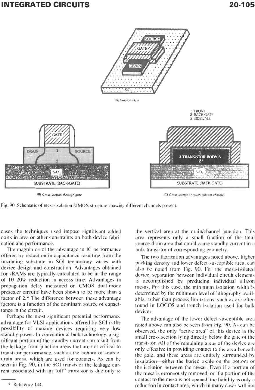
90.
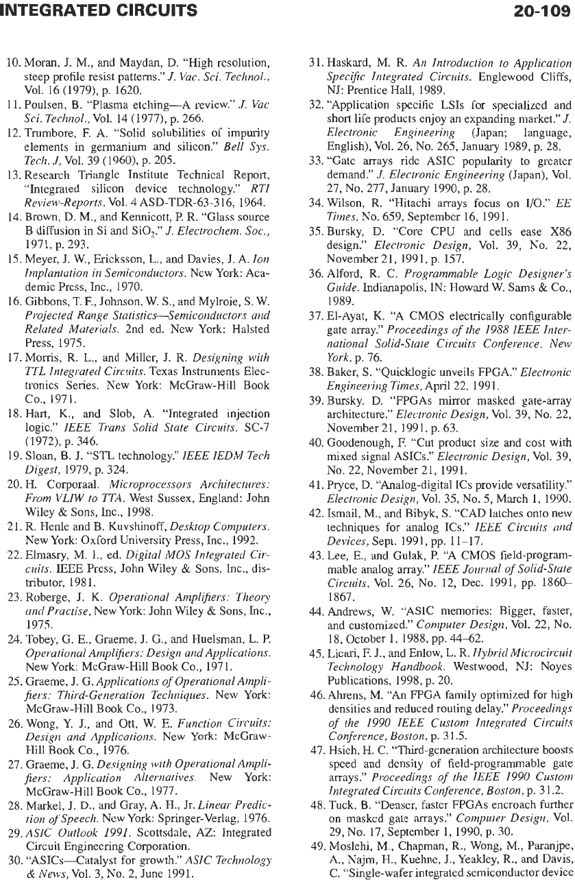
Fig.
90A
shows a surface view of the device; Fig.
90B
shows a cross section through the gate; and Fig.
90C
shows a cross section through the current flow chan-
nel.
This
device is constructed in a “mesa” format,
where
the
individual transistors are built on separated
single-crystal silicon islands formed on the buried
oxide. This construction is uniquely allowed in
SO1
technology by the use of the insulated substrate to pro-
ducer dielectric isolation between devices fabricated in
the silicon islands. The first performance advantages
noted above are reduced susceptibility to the effects of
high-energy particles and resistance to high-dose
X
rays. These features are a direct consequence of the
minimum charge collection volume available for an
SOT
device. This is apparent from Fig.
90,
where only
the volume bounded by the gate, buried oxide, and
junction edges produces susceptibility to charge gener-
ation. This compares to the bulk case where there is a
much larger depletion region, as well as the possibility
of charge collection from the volume below the
depleted area.
Since
SO1
transistors
are
completely dielectrically
isolated, the advantages of no latchup and minimum
parasitic capacitance are “built-in” for this construc-
tion. The advantage of no latchup is significant, partic-
ularly as smaller geometries are considered. Although
various techniques are being considered to eliminate
latchup in minimum-geometry bulk devices, in many
INTEGRATED CIRCUITS
20-1
05
I
SUBSTRATE
(BACK-GATE)
I
1.
FROM
2.
BACKGATE
3.
SIDEWALL
I
SL
BSTRATE
[BACK GATF
J
I
(E)
Cross
sectlon through gate.
(Cj
Cross
&Ion through current channel
Fig.
90.
Schematic of mesa-isolation
SlMOX
structure showing different channels present.
cases the techniques used impose significant added
costs in area or other constraints on both device fabri-
cation and performance.
The magnitude of the advantage to IC performance
offered by reduction in capacitance resulting from the
insulating substrate in
SO1
technology varies with
device design and construction. Advantages obtained
for sRAMs are typically calculated to be in the range
of
10-20%
reduction in access time. Advantages in
propagation delay measured on CMOS dual-mode
prescaler circuits have been shown to be more than a
factor of
2.*
The difference between these advantage
factors is a function of the dominant source of capaci-
tance in the circuit.
Perhaps the most significant potential performance
advantage for
VLSI
applications offered by
SO1
is the
possibility of making devices requiring very low
standby power. In conventional bulk technology, a sig-
nificant portion of the standby current can result from
the leakage from junction areas that are not critical to
transistor performance, such as the bottom of source-
drain areas, which are used for contacts. As can
be
seen in Fig.
90,
in the
SO1
transistor the leakage cur-
rent associated with an
“off’
transistor is due only to
*
Reference
144
the vertical area at the draidchannel junction. This
area represents only a small fraction of the total
source-drain area that could cause standby current in a
bulk transistor of corresponding geometry.
The
two fabrication advantages noted above, higher
packing density and lower defect-susceptible area, can
also be noted from Fig.
90.
For the mesa-isolated
device, separation between individual circuit elements
is accomplished by producing individual silicon
mesas. For this case, the minimum isolation width is
determined by the minimum level of lithography avail-
able, rather than process limitations, such as are often
found in
LOCOS
and trench isolation used for bulk
devices.
The advantage of the lower defect-susceptible area
noted above can also be seen from Fig.
90.
As
can be
observed, the only “active area” of this device is the
small cross section lying directly below the gate of the
transistor. All of the remaining areas of the device are
only effective in providing contact to the area beneath
the gate, and these areas are entirely surrounded by
insulation-ither the buried oxide on the bottom or
the isolation between the mesas. Even if a portion
of
the mesa is erroneously removed, or if a portion of the
contact to the mesa is not opened, the liability
iq
only a
reduction in contact area, which in many cases will not
20-1
06
REFERENCE
DATA
FOR ENGINEERS
significantly impact the device performance. Compare
this situation with the bulk silicon case. In this situa-
tion, the entire area beneath both of the junctions that
comprise the source and drain are critical areas, and
any defect in the silicon in this area, or lithography
defect that erroneously opens these areas, will cause a
fatal flaw in the resulting circuit. This difference in
“active area” between the SO1 device and the usual
bulk technologies can be extremely significant in pro-
viding the ability to produce adequate yield on
advanced large-area, high-performance structures.
Devices
on
SO1
The electrical performance of bipolar devices on
SO1 materials is similar to that of bipolar devices on
bulk material, with the advantage of reduced capaci-
tance and reduced susceptibility to latchup and upset
by radiation sources.
CMOS
devices in
SO1
materials
may be fabricated to operate in two different modes.”
These are designated as “fully depleted” and “nonfully
depleted” devices. From a physical standpoint, the dif-
ference between these two configurations is that in the
nonfully depleted device the
SO1
film is doped
in
such
a way that in operation a neutral region exists between
the front and back gate depletion regions, thus elirn-
*
Reference
145.
nating coupling between the two parallel
MOS
devices
making up the
SO1
transistor. In the fully depleted
case, there is no neutral region between the two paral-
lel devices, and direct coupling exists between the
front gate and the back gate of the SO1 device.
Nonfully
Depleted Devices
The electrical characteristics of nonfully depleted
CMOS/SOI devices are similar to those of bulk
devices, with two distinct differences: the appearance
of a “kink effect” and enhanced subthreshold slope.
Both of these effects are directly related to the fact that
the body of the
SO1
transistor is electrically “floating”
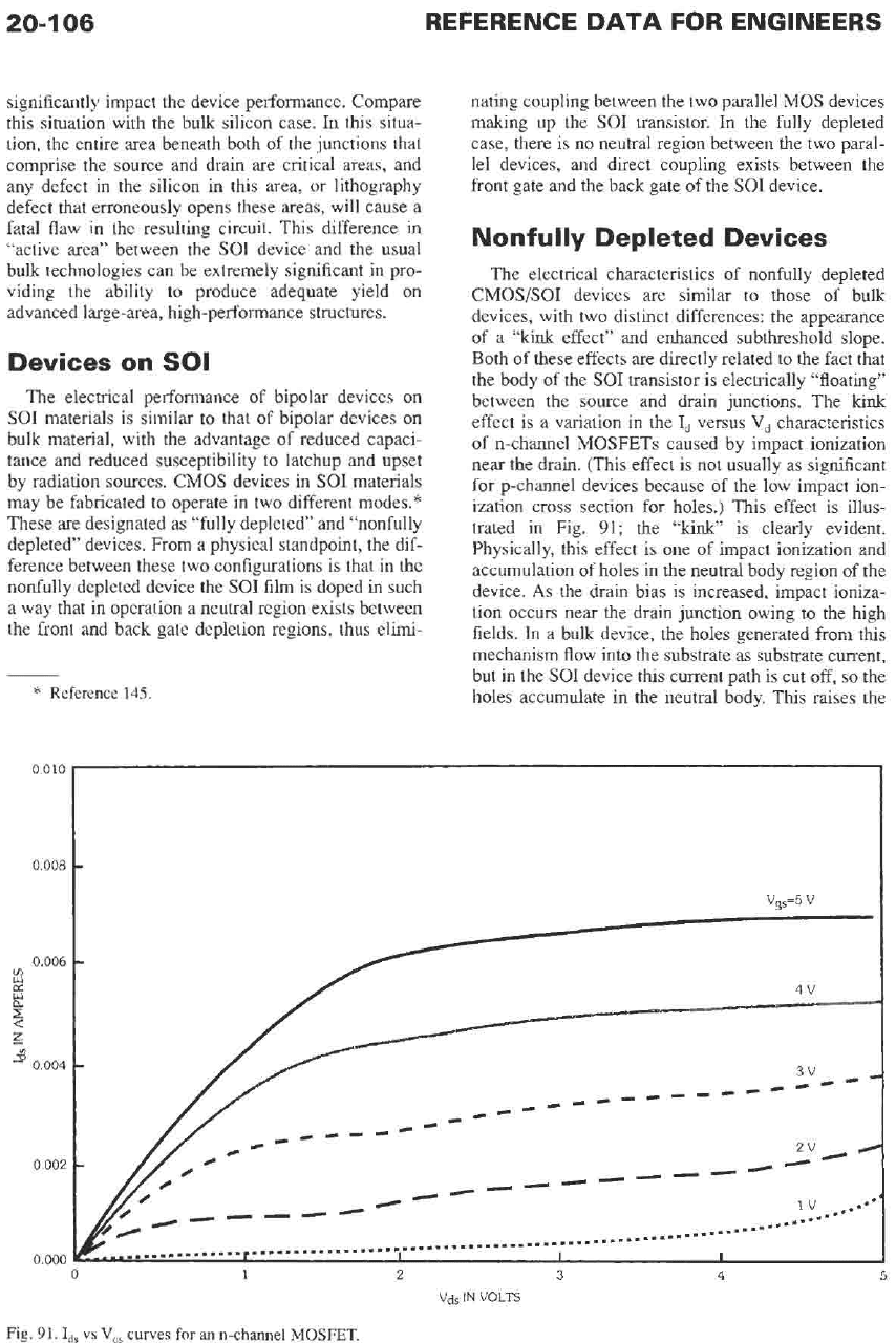
between the source and drain junctions. The
kink
effect is a variation in the
I,
versus
V,
characteristics
of n-channel MOSFETs caused by impact ionization
near the drain. (This effect is not usually as significant
for p-channel devices because of the low impact ion-
ization cross section for holes.) This effect is illus-
trated in Fig.
91;
the “kink” is clearly evident.
Physically, this effect
is
one of impact ionization and
accumulation of holes in the neutral body region of the
device.
As
the drain bias is increased, impact ioniza-
tion occurs near the drain junction owing
to
the high
fields. In a bulk device, the holes generated from this
mechanism flow into the substrate as substrate current,
but in the
SO1
device this current path is cut
off,
so
the
holes accumulate in the neutral body. This raises the
0
010
0
008
0
006
(I)
U
B
z
8
-
0004
2
--------
0
002
----
0
000
0
1
2
3
4
5
v&
IN
VOLTS
Fig.
91.
I,,
vs
V,, curves
for
an n-channel
MOSFET.
20-1
07
body potential, which in turn raises the drain current
through an effective reduction in the threshold voltage
and results in the
“kink”
in the
I,,
versus
V,,
curve.
The kink effect is significantly affected by the body
doping of the device-a higher body doping produces
a more pronounced kink effect in
SO1
devices.
The subthreshold characteristics of
MOS
transistors
on
SO1
materials can also be affected by the floating
body effects. At high
V,,,
the subthreshold current
increases more rapidly with
Vgs
(giving a steeper sub-
threshold slope) because as
Vgs
increases, the weak
inversion current causes ionization near the drain. The
holes accumulated in the body from this impact ioniza-
tion raise the body potential, resulting in a faster
increase of the drain current with
Vgs
than would oth-
erwise occur.
In
many device structures the kink effect and
enhanced subthreshold slope are not significant limita-
tions. However, since these features become more pro-
nounced for smaller geometries, significant efforts
on
“drain engineering” are used to minimize these effects.
Fully Depleted Devices
When the thickness of the silicon film is thinner
than the combined depletion regions of the two paral-
lel
MOS
transistors making up an
SO1
device, the
V,
is
not substantially influenced by the body potential, thus
eliminating the
kink
effect.
In
addition, other advan-
tages of the fully depleted configuration are higher
drive current, reduced hot-carrier effects, and reduced
short-channel characteristics.
Nigh drive current in completely depleted
SO1
tran-
sistors is a result of lower channel doping, increased
mobility due to lower vertical electric fields, and a
more effective use of gate voltage to influence inver-
sion charge.
In
a fully depleted device, a portion of the
surface transistor gate voltage drop occurs across the
active device film, and a portion of the drop is across
the buried oxide and substrate.
In
this case, the vertical
electric field is lower in the completely depleted device
than it is
in
a comparable bulk device, which results in
an increased mobility and increased current.
In
addi-
tion,
in
the presence of the buried oxide the changes in
the gate voltage are more significantly reflected in the
inversion charge than is the case for a bulk device. This
results in an even greater increase in drive current. Cal-
culations show that a
20%
to
50%
increase
in
drive
current over comparable bulk devices is available with
fully depleted technology.
The inverse subthreshold slope of fully depleted
SO1
transistors is typically smaller (resulting in faster
turn-on)
than that for comparable geometry bulk or
nonfully depleted
SO1
devices.
In
bulk and nonfully
depleted
SO1
devices, a change in the value
of
Vss
is
reflected
in
a change
in
the voltage drop over the gate
oxide and the depletion region in a ratio determined by
the capacitive voltage divider between these two
device components.
In
the usual construction of fully
depleted devices, however, changes
in
Vg,
occur
mostly over the buried oxide, since there is no change
in the depletion charge in the silicon film. This results
in a much higher percentage of
Vgs
being reflected in
changes in the surface potential of the device, and
therefore a much smaller inverse subthreshold slope
and faster turn-on characteristics. This rapid
turn-on
of
completely depleted
SO1
devices, coupled with the
availability of high current drive, makes this technol-
ogy ideally suited for high-performance, low-voltage
circuit applications.
SO1
Circuits
A major drive for the initial development of
SO1
integrated circuits was applications in radiation hard-
ened
CMOS
memory devices for defense applications.
Prior to
SOI,
radiation hardened memory circuits were
fabricated
on
silicon on sapphire substrates. These
devices performed well in radiation environments, but
the silicon on sapphire substrates typically had defect
densities that were too high to use in fabrication of
VLSI
circuits, and they were too brittle to be
run
in
standard silicon fabrication lines. The initial
SO1
VLSI
devices were memories, produced to densities from 64
Kbits to
1
Mbit, fabricated
on
standard
VLSI
fabrica-
tion facilities with high yield and excellent radiation
hardness.* These devices demonstrated the advantage
of
SO1
over the prior silicon
on
sapphire technology.
The above-mentioned
ICs
were produced using non-
fully depleted
SO1
technology.
Various
circuits have
been fabricated using fully depleted transistors, and in
all
cases results superior to comparable bulk
ICs
have
been achieved. A 16K sRAM fabricated as both a com-
pletely depleted
SO1
device and as a bulk device has
shown a 40% increase in speed for the completely
depleted structure. A high-speed CMOS prescaler cir-
cuit was built in completely depleted
SIMOX
and was
found to operate
50%
faster than a comparable bulk
device. In addition, completely depleted devices with
excellent short-channel characteristics at gate lengths
below
0.5
pm have recently been discussed.?
SO1
based devices received their first major com-
mercial introduction in the year
2000
in
the form of
advanced microprocessors for
IBM
server applica-
tions. These systems provide a
20%
performance
advantage because of the use of
SO1
devices. The
SO1
device used is designated the AS400 processor. This
device operates in the partially depleted
SO1
mode,
and employs design features uniquely applicable to
SO1
circuits.
This
effort not only demonstrates that
partially depleted
SO1
circuits can be fabricated in
usual
IC
manufacturing environments, but it also
shows examples where
SO1
unique features can be
exploited for a larger performance gain than achiev-
able through a simple bulk-to-SO1 re-map. Several
*
Reference
146.
t
Reference
147.
20-1
08
REFERENCE
DATA
FOR ENGINEERS
other microprocessor manufacturers have announced
plans to follow the IBM lead.
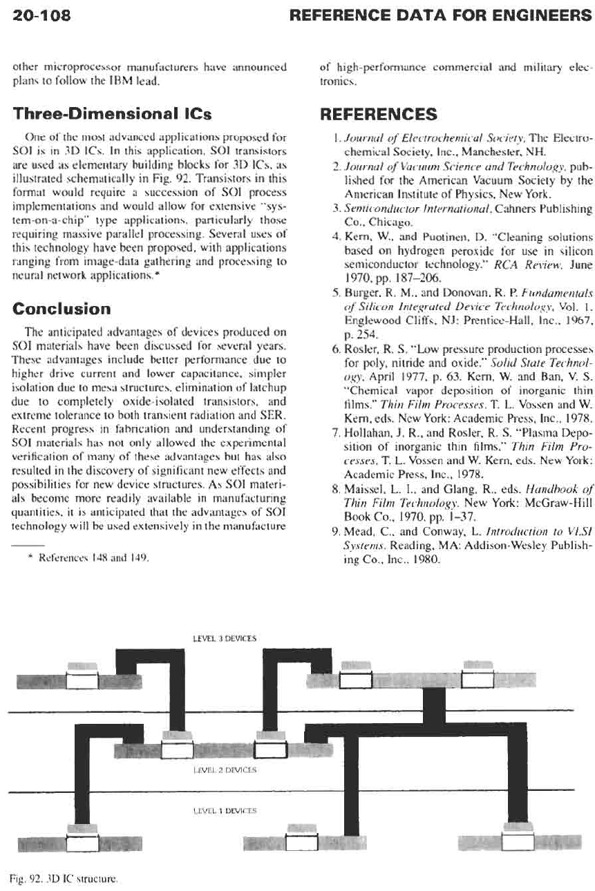
Three-Dimensional ICs
One
of
the most advanced applications proposed for
SO1 is in 3D ICs. In this application,
SOT
transistors
are
used as elementary building blocks for
3D
ICs, as
illustrated schematically in Fig. 92. Transistors in this
format would require a succession
of
SOT
process
implementations and would allow for extensive “sys-
tem-on-a-chip”
type
applications, particularly those
requiring massive parallel processing. Several uses of
this technology have been proposed, with applications
ranging from image-data gathering and processing to
neural network applications.*
Conclusion
The anticipated advantages of devices produced on
SO1 materials have been discussed for several years.
These advantages include better performance due to
higher drive current and lower capacitance, simpler
isolation due to mesa structures, elimination of latchup
due to completely oxide-isolated transistors, and
extreme tolerance to both transient radiation and SER.
Recent progress in fabrication and understanding of
SO1 materials has not only allowed the experimental
verification of many of these advantages but has also
resulted in the discovery
of
significant new effects and
possibilities for new device structures. As SO1 materi-
als
become more readily available in manufacturing
quantities, it is anticipated that the advantages of
SO1
technology will
be
used extensively in the manufacture
*
References
148
and
149.
of
high-performance commercial and military elec-
tronics.
REFERENCES
1.
Journal
of
Electrochemical Society,
The Electro-
chemical Society, Inc., Manchester,
NH.
2.
Journal
of
Vacuum Science and Technology,
pub-
lished for the American Vacuum Society by the
American Institute of Physics, New York.
3.
Semiconductor International,
Cahners Publishing
Co., Chicago.
4.
Kern, W., and Puotinen, D. “Cleaning solutions
based on hydrogen peroxide for use in silicon
semiconductor technology.”
RCA Review,
June
5. Burger, R. M., and Donovan,
R.
P.
Fundamentals
of
Silicon Integrated Device Technology,
Vol. 1.
Englewood Cliffs, NJ: Prentice-Hall, Inc., 1967,
p. 254.
6.
Rosler, R.
S.
“Low pressure production processes
for
poly,
nitride and oxide.”
Solid State Technol-
ogy,
April 1977, p.
63.
Kern, W. and Ban, V.
S.
“Chemical vapor deposition of inorganic thin
films.”
Thin Film Processes,
T.
L.
Vossen and
W.
Kern, eds. New
Yo&
Academic
Press,
Inc., 1978.
7. Hollahan, J. R., and Rosler, R.
S.
“Plasma Depo-
sition of inorganic thin films.”
Thin Film Pro-
cesses,
T.
L.
Vossen and
w.
Kern,
eds.
New York
Academic
Press,
Inc., 1978.
8.
Maissel,
L.
I., and Glang, R., eds.
Handbook
of
Thin Film Technology.
New York: McGraw-Hill
9. Mead, C., and Conway,
L.
Introduction to
VLSI
Systems.
Reading,
MA:
Addison-Wesley Publish-
ing
Co.,
Inc., 1980.
1970, pp. 187-206.
Book CO., 1970, pp. 1-37.
LEVEL
3 DEVICE3
Fig.
92.
3D
IC
structure.
20-1
09
10.
Moran, J. M., and Maydan, D. “High resolution,
steep profile resist patterns.”
J.
Vac. Sci. Technol.,
Vol. 16 (1979), p. 1620.
11. Poulsen, B. “Plasma etching-A review.”
J.
Vac
Sci. Technol.,
Vol. 14 (1977), p. 266.
12. Trumbore,
E
A. “Solid solubilities of impurity
elements
in
germanium and silicon.”
Bell Sys.
Tech.
J,
Vol. 39 (1960), p. 205.
13. Research Triangle Institute Technical Report,
“Integrated silicon device technology.”
RTI
Review-Reports,
Vol. 4 ASD-TDR-63-3 16, 1964.
14. Brown, D.
M.,
and Kennicott, P.
R.
“Glass source
B diffusion in Si and SiO,.”
J.
Electrochem. Soc.,
1971, p. 293.
15. Meyer, J. W., Ericksson, L., and Davies, J. A.
Ion
Implantation in Semiconductors.
New York: Aca-
demic
Press,
Inc., 1970.
16. Gibbons, T. F., Johnson, W.
S.,
and Mylroie,
S.
W.
Projected Range
Statistics4emiconductors
and
Related Materials.
2nd ed. New York Halsted
Press, 1975.
17. Morris, R.
L.,
and Miller, J.
R.
Designing with
TTL
Integrated Circuits.
Texas Instruments Elec-
tronics Series. New York: McGraw-Hill Book
Co., 1971.
18. Hart,
K.,
and Slob, A. “Integrated injection
logic.”
IEEE Trans Solid State Circuits,
SC-7
(1972), p. 346.
19. Sloan, B. J.
“STL
technology.”
IEEE IEDM Tech
Digest,
1979, p. 324.
20. H. Corporaal.
Microprocessors Architectures:
From VLIW to
TTA.
West Sussex, England: John
Wiley
&
Sons, Inc., 1998.
21. R. Henle and
B.
Kuvshinoff,
Desktop Computers.
New York: Oxford University Press, Inc., 1992.
22. Elmasry, M.
I.,
ed.
Digital MOS Integrated Cir-
cuits.
IEEE Press, John Wiley
&
Sons, Inc., dis-
tributor, 1981.
23. Roberge, J.
K.
Operational Amplifiers: Theory
and Practise,
New York John Wiley
&
Sons, Inc.,
1975.
24. Tobey, G. E., Graeme, J. G., and Huelsman,
L.
P.
Operational Amplifiers: Design and Applications.
New York: McGraw-Hill Book Co., 1971.
25. Graeme, J. G.
Applications
of
Operational Ampli-
fiers: Third-Generation Techniques.
New York
McGraw-Hill Book Co., 1973.
26. Wong, Y. J., and Ott, W.
E.
Function Circuits:
Design and Applications.
New York: McGraw-
Hill Book Co., 1976.
27. Graeme, J.
G.
Designing with Operational Ampli-
fiers: Application Alternatives.
New York:
McGraw-Hill Book Co., 1977.
28. Markel, J. D., and Gray, A. H., Jr.
Linear Predic-
tion of Speech.
New York Springer-Verlag, 1976.
29.
ASIC Outlook
1991.
Scottsdale, AZ: Integrated
Circuit Engineering Corporation.
30. “ASICs-Catalyst for growth.”
ASIC Technology
&News,
Vol. 3, No. 2, June 1991.
31. Haskard, M.
R.
An Introduction to Application
Speciftc Integrated Circuits.
Englewood Cliffs,
NJ: Prentice Hall, 1989.
32. “Application specific LSIs for specialized and
short life products enjoy an expanding market.”/.
Electronic Engineering
(Japan; language,
English), Vol. 26, No. 265, January 1989, p. 28.
33. “Gate arrays ride ASIC popularity
to
greater
demand.”
J.
Electronic Engineering
(Japan), Vol.
27, No. 277, January 1990, p. 28.
34. Wilson, R. “Hitachi arrays focus on I/O.”
EE
Times,
No. 659, September 16, 1991.
35.Bursky,
D. “Core CPU and cells ease X86
design.”
Electronic Design,
Vol. 39, No. 22,
November 21, 1991, p. 157.
36. Alford,
R.
C.
Programmable Logic Designer’s
Guide.
Indianapolis, IN: Howard W. Sams
&
Co.,
1989.
37. El-Ayat, K. “A CMOS electrically configurable
gate array.”
Proceedings
of
the
1988
IEEE Inter-
national Solid-state Circuits Conference, New
York,
p. 76.
38. Baker,
S.
“Quicklogic unveils FPGA.”
Electronic
Engineering Times,
April 22, 1991.
39. Bursky, D. “FPGAs mirror masked gate-array
architecture.”
Electronic Design,
Vol. 39, No. 22,
November 21, 1991, p. 63.
40. Goodenough, F. “Cut product size and cost with
mixed signal ASICs.”
Electronic Design,
Vol. 39,
No. 22, November 21, 1991.
41. Pryce, D. “Analog-digital ICs provide versatility.”
Electronic Design,
Vol. 35, No. 5, March 1, 1990.
42. Ismail, M., and Bibyk, S. “CAD latches onto new
techniques for analog ICs.”
IEEE Circuits and
Devices,
Sept. 1991, pp. 11-17.
43. Lee,
E.,
and Gulak, P. “A CMOS field-program-
mable analog array.”
IEEE Journal
of
Solid-state
Circuits,
Vol. 26, No. 12, Dec. 1991, pp. 1860-
1867.
44. Andrews, W. “ASIC memories: Bigger, faster,
and customized.”
Computer Design,
Vol. 22, No.
18, October
1,
1988, pp. 44-62.
45. Licari, F. J., and Enlow, L. R.
Hybrid Microcircuit
Technology Handbook.
Westwood, NJ: Noyes
Publications, 1998, p. 20.
46. Ahrens, M. “An FPGA family optimized for high
densities and reduced routing delay.”
Proceedings
of
the
1990
IEEE Custom Integrated Circuits
Conference, Boston,
p. 31.5.
47. Hsieh,
H.
C. “Third-generation architecture boosts
speed and density
of
field-programmable gate
arrays.”
Proceedings
of
the
IEEE
1990
Custom
Integrated Circuits Conference, Boston,
p. 3 1.2.
48. Tuck, B. “Denser, faster FPGAs encroach further
on masked gate arrays.”
Computer Design,
Vol.
29, No. 17, September 1, 1990, p. 30.
49. Moslehi, M., Chapman, R., Wong, M., Paranjpe,
A.,
Najm, H., Kuehne,
J.,
Yeakley,
R.,
and Davis,
C. “Single-wafer integrated semiconductor device