Middleton W.M. (ed.) Reference Data for Engineers: Radio, Electronics, Computer and Communications
Подождите немного. Документ загружается.


20-70
REFERENCE
DATA
FOR
ENGINEERS
200
I
I
I
I
I
I
I
I
I
0
20
40
60
80
100
120 140
TIME
IN
SECONDS
Fig. 65. Open-loop temperature-vs-time characteristics of a 150-mm wafer heated using a
three-zone
RTP
illuminator
with
opti-
mum
zone
power ratios.
ing of any optical chamber windows through which the
wafer radiance is monitored, and any ensuing changes
in the window index of refraction and transmission
characteristics, must be corrected for in the measured
radiance. Without proper compensation, these factors
can result in large temperature-measurement errors.
Frequent calibrations against thermocouple instru-
mented wafers have allowed somewhat improved tem-
perature control for a specific process/reactor but are
not satisfactory
in
general. Preprocess measurement of
wafer reflectance and backside roughness may be used
to correct for wafer-to-wafer changes in surface optical
conditions. The use of preprocess wafer reflectance
measurements has been reported for improved pyrom-
etry measurements.
*
Real-time wafer emissivity mea-
surement has been developed to allow correction for
emissivity changes. Aside from the above issues
affecting pyrometry measurement accuracy and
repeatability, wafer temperature uniformity is a key
requirement to prevent slip dislocations in high-tem-
perature RE?? Multipoint fiber-optic pyrometry
allows real-time monitoring and control of wafer tem-
perature using multizone lamp heat sources.$
Fig.
66
is a schematic diagram of a three-zone lamp-
heated RTCVD reactor with multipoint temperature
measurement and control. The wafer is processed face-
down to minimize particulate deposition on the device
side.
A
three-zone tungsten-halogen lamp source pro-
vides radiant heating to the back side
of
the
wafer.
A
quartz window provides a vacuum seal and allows for
optical access
to
the wafer. Multiple pyrometers
are
arranged at various radial positions, each looking at
the
back side
of
the wafer through a 3.3-pm interfer-
ence filter and a suitable fiber light pipe. The light pipe
is water cooled to prevent excessive heating caused by
reflection and radiation from the hot wafer. The
pyrometerflight pipe assembly detail is shown in Fig.
67.
The light pipe material used for 3.3-pm transmis-
sion is either a sapphire rod or
a
fluoride fiber bundle.
t
Reference
52.
$.
Reference
51.
*
Reference
58.

INTEGRATED CIRCUITS
20-7
1
I
Ill
U
I
I
i"
I
UIU
I
Fig.
66.
Schematic diagram
of
an
RTCVD
reactor used
for
tungsten deposition.
Various
sensors
are
shown
for
temperature moni-
toring and
CVD-W
process control.

20-72
REFERENCE
DATA
FOR ENGINEERS
COOUNG
WATER
SUPPLY
OUTER
3/8"
-
Fig.
67.
Detail of a water-cooled light pipe, filter, and pyrometer assembly for multipoint temperature measurement.
The temperature of the water-cooled light-pipe tip,
facing
the
wafer,
is
maintained at less than
SO
"C.
The
temperature readout from each pyrometer is relayed to
the process equipment with the process computer pro-
viding a temperature set-point to the controller. Any
corrections for surface roughness, emissivity, lamp
interference, or window temperature
are
then used to
correct the pyrometer temperature reading.
The real-time emissivity measurement system is
shown in Fig.
68.*
This technique involves the use of a
chopped
CO
laser beam, at 5.4 pm, to probe the wafer
back-side surface during processing. This choice of
wavelength eliminates the measurement of reflected
lamp light, since the quartz jackets of the tungsten-
*
Reference
5
1.
halogen lamp bulbs provide a necessary cutoff of
direct
filament
light at above
3.5
pm.
The incident
laser beam power is measured
using
a
ZnSe
beam
splitter and
an
infrared
(IR)
detector.
The
light trans-
mitted through the beam splitter is then focused onto a
chalcogenide fiber and transmitted to
the
probe tip at
the wafer end. Light that leaves the fiber tip and is
transmitted through the chamber window arrives at the
wafer. The chamber window is typically fused
quartz,
which has a small thermal expansion coefficient. The
window material where the 5.4-pm
beam
is incident,
however, needs
to
allow maximum transmission at this
wavelength.
A
thin
(1 mm) sapphire section is ideal,
given the inertness of sapphire. The light arriving at
the wafer surface is partly reflected, absorbed, or trans-
mitted. Since the transmitted portion is essentially

INTEGRATED
CIRCUITS
20-73
CHALCOGENIDE
FIBER
BUNDLE
WAFER
Fig.
68.
Schematic
of a
5.4-pm
laser based emissivity and temperature measurement system, using chalcogenide
IR
fiber.
eliminated above 6OC!-70O0C, it can be neglected in
most RTP applications. Additional optical hardware
can be arranged to measure the transmitted portion if
the operating temperature is sufficiently low. However,
the transmission measurements are not required at all
if the semiconductor substrates are heavily doped (e.g.,
p-/p' epi material used for CMOSBiCMOS technolo-
gies). Therefore, with the transmission neglected, the
reflected light
is
collected via a fiber bundle arrange-
ment at the probe tip and relayed back to a suitable
detector. Spectral wafer emissivity can be extracted
based on measurements of the reflected and the inci-
dent beam power levels. The reflected beam detector
is
also used
to
measure the light emitted by the heated
wafer at the 5.4-pm wavelength, such that radiance
and emissivity are measured simultaneously, allowing
precise calculation of wafer temperature.
It is essential
to
note that the surface roughness of
the back side
of
the wafer affects the measurement of
the reflected light, since the scattering profile
of
the
reflected light generally depends on the surface rough-
ness. The reflection from a typical wafer back side at
5.4
pm contains a strong specular component, with a
smaller but significant diffuse component. The diffuse
component is not measured by the reflection bundle:
consequently, a preprocess surface roughness mea-
surement is used to provide a ratio of expected diffuse-
to-specular reflection.
Fiber-optic
Scatter Sensor-The optical reflec-
tion and transmission properties of semiconductor
wafers have important effects on various process vari-
ables such as wafer temperature, dynamics of wafer
heating and cooling, and fabrication process unifor-
mity in RTP. For instance, knowledge of these proper-
ties is required to evaluate substrate emissivity and
temperature. Reflection and transmission parameters
depend not only on the intrinsic properties of the sur-
face films but also on the roughness present on the
wafer surface. Surface roughness may be due to the
wafer back side or a polycrystalline film present on the
wafer (front side or back side). Reflection and trans-
mission of wafers with a smooth surface will be essen-
tially specular or coherent.
In
wafers with a rough
surface film (or a rough back side), only a fraction of
the reflected signal will be specular; the remaining
fraction will be scattered within a space cone angle
around the specular direction. The latter will increase
as the surface roughness increases (or the light wave-
length decreases). Surface roughness can also have an
effect on the substrate emissivity and should be taken
into consideration in any real-time pyrometry-based
temperature sensor. In situ preprocess/postprocess
measurement of the surface scattering characteristics
and reflection properties of a wafer can be used
to
monitor
its
surface roughness and spectral emissivity.
An important application of
this
technique is that mea-
surement of these properties can be used in the real-
time determination of the emissivity and temperature
of a silicon substrate at different steps during a process
flow. Another important application relates to mea-
surements of CVD films
on
silicon wafers. For
20-74
instance, it has been shown that surface roughness of
LPCVD W films is directly proportional to the film
thickness.* Thus, an in situ noninvasive sensor that can
evaluate surface roughness and spectral reflectance of
semiconductor wafers can be used as a tool
to
monitor
thickness and quality of LPCVD W (and other poly-
crystalline films). This can be done both for process
control and for process prognosis/diagnosis purposes.
An in situ sensor to determine surface roughness,
reflectance, and spectral emissivity of silicon wafers
with various surface films has been developed.? The
sensor has been designed for implementation in the
vacuum load-lock chambers of SWP reactors. Opera-
tion of this in situ sensor is based on the relation
between the surface roughness and the specular and
scattered reflection properties of semiconductor wafers
for an incident monochromatic electromagnetic wave.
Thus, measurement of the total reflectivity as well as
the scattering and specular parameters can be corre-
lated to surface roughness and spectral emissivity of
silicon substrates with various surface films. These
parameters depend on the type and thickness of films
on both the front side and back side of these substrates.
Metal Sheet Resistance Sensor-Wafer-to-wafer
repeatability of CVD processes including CVD metal
is of primary concern in ULSI manufacturing. This
subsection describes a sensor device that can perform
real-time monitoring
of
the CVD metal process with a
high degree of accuracy and reliability.$. A variation of
the well-known four-point probe technique commonly
used to measure metal-film sheet resistances ex situ
has been employed to measure the mean sheet resis-
tance of blanket metal films across the entire wafer
during metal CVD. These measurements are used to
determine the deposition process end point, thus
improving wafer-to-wafer repeatability compared
to
standard timed process end points. This method differs
from four-point probe measurements in that the driv-
ing current is passed between the same probe points
across which the voltage drop is measured. As the cur-
rent is passing through the voltage measurement
probes, there is an inherent contact potential between
the probe and the measurement surface. This technique
is viable only if this contact potential is repeatable
enough to be accounted for in the conversion algo-
rithm. Extensive experimentation indicates that this is
indeed the case.
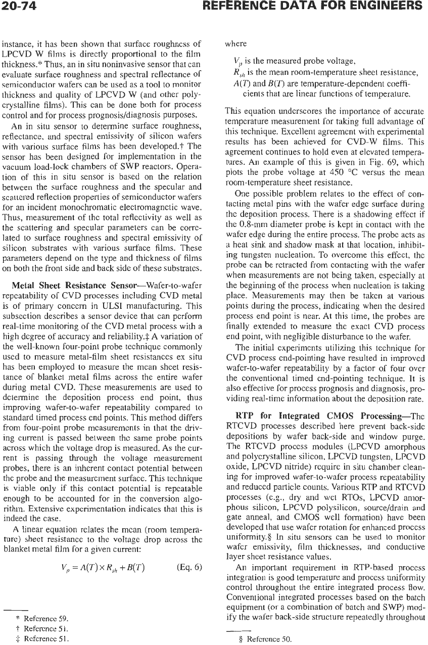
A linear equation relates the mean (room tempera-
ture) sheet resistance
to
the voltage drop across the
blanket metal film for a given current:
V,
=
A(T)
x
R,,
+
B(T)
*
Reference
59.
t
Reference
5
1.
i
Reference
5
1.
where
Vp
is the measured probe voltage,
R,,
is the mean room-temperature sheet resistance,
A(T)
and
B(T)
are temperature-dependent coeffi-
cients that are linear functions of temperature.
This equation underscores the importance of accurate
temperature measurement for taking full advantage of
this technique. Excellent agreement with experimental
results has been achieved for CVD-W films. This
agreement continues to hold even at elevated tempera-
tures.
An
example of
this
is given in Fig.
69,
which
plots the probe voltage at
450
"C versus the mean
room-temperature sheet resistance.
One possible problem relates
to
the effect of con-
tacting metal pins with the wafer edge surface during
the deposition process. There is a shadowing effect if
the 0.8-mm diameter probe is kept in contact with the
wafer edge during the entire process. The probe acts as
a heat
sink
and shadow mask at that location, inhibit-
ing tungsten nucleation. To overcome this effect, the
probe can be retracted from contacting with the wafer
when measurements are not being taken, especially at
the beginning of the process when nucleation is taking
place. Measurements may then be taken at various
points during the process, indicating when the desired
process end point is near. At this time, the probes are
finally extended to measure the exact CVD process
end point, with negligible disturbance to the wafer.
The initial experiments utilizing this technique for
CVD process end-pointing have resulted
in
improved
wafer-to-wafer repeatability by a factor of four over
the conventional timed end-pointing technique. It is
also
effective for process prognosis and diagnosis, pro-
viding real-time information about the deposition rate.
RTP for Integrated
CMOS
Processing-The
RTCVD processes described here prevent back-side
depositions by wafer back-side and window purge.
The RTCVD process modules (LPCVD amorphous
and polycrystalline silicon, LPCVD tungsten, LPCVD
oxide, LPCVD nitride) require in situ chamber clean-
ing for improved wafer-to-wafer process repeatability
and reduced particle counts. Various RTP and RTCVD
processes (e.g., dry and wet RTOs, LPCVD amor-
phous silicon, LPCVD polysilicou, sourcetdrain
and
gate anneal, and CMOS well formation) have been
developed that use wafer rotation for enhanced process
uniformity.§
In
situ sensors can be used to monitor
wafer emissivity, film thicknesses, and conductive
layer sheet resistance values.
An
important requirement in RTP-based process
integration is good temperature and process uniformity
control throughout the entire integrated process flow.
Conventional integrated processes based
on
the batch
equipment (or a combination of batch and
SWP)
mod-
ify the wafer back-side structure repeatedly throughout
5
Reference
50.

INTEGRATED
ClRC
U
ITS
20-75
Fig.
69.
Two-point probe voltage
at
450
"C vs
the
mean
room-temperature tungsten
sheet
resistance.
the process flow. For instance, at various process steps
the wafer back sides may be bare or may have a com-
bination of silicon dioxide, silicon nitride, and/or poly-
silicon layers. Moreover, the thicknesses of these
layers can vary as the process flow proceeds owing to
many wafer cleaning and etch processes (wet and
plasma). The integrated process flow can also cause
back-side layer thickness nonuniformities. These vari-
ations translate into large-scale wafer back-side emis-
sivity changes, which can cause significant RTP
temperature and uniformity control problems. The
process-control difficulties can be somewhat alleviated
by using multipoint pyrometry with real-time emissiv-
ity compensation. Even with emissivity compensation,
the wafer back-side nonuniformities can degrade RTP
uniformity as the result of distorted or modified optical
energy absorption and radiative losses.
To
minimize the above-mentioned complications, a
sub-0.50 pm CMOS process integration has been per-
formed that uses starting silicon wafers with custom-
ized back-side seal layers.*
The
p-
epi/p' wafers
are
p-ocessed to receive a uniform back-side stack of
1300
A
silicon nitride on
1000
A
silicon dioxide. This back-
side seal serves several useful purposes.
(1)
It prevents
dopant outdiffusion from the heavily doped substrate;
(2)
it prevents back-side emissivity variations during
oxidation and oxide deglaze processes (due to the oxi-
dation and etch resistance of silicon nitride); and
(3)
it
ensures uniform and stable back-side emissivity
throughout the entire integrated RTP-based process
flow. It should be emphasized that the one-sided depo-
sitions
in
RTCVD processes help to maintain a rela-
tively constant and uniform back-side emissivity on the
wafers
in
process. The above-mentioned back-seal pro-
cess also eliminates any process nonuniformities
caused by nonuniform wafer emissivities. Small wafer-
to-wafer back-side emissivity variations
are
easily
tracked and compensated via suitable
in
situ sensors.
All the RTP-based processes described here employ
reflective showerheads facing the front side of the
wafer.
As
a result, the front-side pattern effects
on
pro-
cess uniformity are essentially eliminated (as the result
of the optical black-body cavity produced between the
wafer front side and the reflective showerhead).
Numerous RTP-based fabrication processes have
been developed for an SWP-based sub-0.5 pm twin-
well double-level metal CMOS technology.? Fig.
70
shows a schematic cross-sectional view of this tech-
nology. Two technology versions have been investi-
gated: one has buried-channel PMOS and surface-
channel NMOS transistors without salicide and with
silicided contacts; the other has surface-channel
NMOS
and PMOS transistors with salicide. This
device cross section shows multiple RTP-fabricated
device regions including:
(1)
gate electrode (LPCVD
amorphous and polycrystalline silicon),
(2)
gate
*
Reference
50.
t
Reference
50.

20-76
REFERENCE
DATA
FOR ENGINEERS
PECVD
TEOS
BPSG
"1
-,
p*'
SUBSTRATE
___._I_~
___-----
___
Fig.
70.
Schematic cross-sectional diagram of a
sub-O.50
pm
RTP-based
CMOS
technology.
dielectric (dry RTO),
(3)
n and p wells (wet RTO for
initial oxide and RTP oxynitridation-enhanced diffi-
sion for well formation),
(4)
source/drain junctions
(S/D
RTA),
(5)
silicided contacts
(RTF'
silicide react),
(6)
poly-buffer-LOCOS
or
PBL isolation (LPCVD sil-
icon nitride on LPCVD polysilicon on dry RTO oxide
oxidation mask),
(7)
oxide spacers (LPCVD silicon
dioxide),
(8)
RTP forming gas anneal, and (9) double-
level metal system (includes LPCVD tungsten). The
total number of RTP steps (depositions, oxidations,
and anneals) in the integrated CMOS flow exceeds
15.
A
single-wafer RTCVD-based epitaxial growth pro-
cess was also developed for blanket boron-doped epi-
taxial silicon deposition to fabricate starting epitaxial
wafers.*
RTP-Based
Process
Development
Overview-
Table
16
shows a list of various RTP-based processes
developed for an integrated sub-0.50 pm CMOS flowt
along with their specific applications and process
parameter domains.
The epitaxial growth process was developed using
SiH2C12 (DCS)/H, chemistry at low pressures
(5-15
torr). A typical in situ-doped process employs an ini-
tial low-temperature
(650-750
"C) in situ oxide
removal process step (Gew,) followed by epitaxial
silicon deposition (DCS/H,/B,H,) at 1000 "C for blan-
ket p- epi on p+ substrate.
*
Reference
49.
t
Reference
50.
The RTO processes
are
used for oxide
growth
in the
thickness range of
75
to
250
A.
Gate oxide
(80
A)
and
PBL initial oxide (90
8)
are
grown by using dry RTO.
It was determined that the
dry
and wet RTO processes
should not be performed in the same process chamber
because of possible cross-contamination and process
memory effects of steam. As a result, dedicated reac-
tors were. used for these
two
processes. The wet RTO
process employs an external pyrogenic steam genera-
tor where
H,
and
O2
flow rates can be controlled. The
wet RTO process is used to grow the initial
250
A
oxide for CMOS well formation. The well implants are
performed through this oxide. Moreover, this oxide
provides the oxynitridation-enhanced diffusion
(ONED) effect for well formation using ammonia
anneal. Wet RTO is also used to grow a sacrificial
(dummy) gate oxide after the isolation process module
and before the dry gate oxidation step. To maintain
reasonable process throughputs, both
dry
and wet RTO
processes
are
performed near the atmospheric pressure
(650
torr). Much lower pressures
are
not acceptable
because the oxidation rates
are
significantly reduced
and the resulting RTO times become excessively long.
Source/drain rapid thermal anneal
(S/D
RTA) is
used for activation and formation
of
shallow p'n and
n+p source/drain junctions. This process is performed
at 950-1000
"C
in argon ambient. Although the pro-
cess can be performed at lower pressures
(1
torr), high
pressures
(650
torr)
are
preferred in order to ensure
sufficient cooling of the showerhead plate facing the
wafer. This choice degrades the process throughput in

20-77
RTP-Based Processes
Epitaxyhn
situ
clean
TABLE
16. RTP-BASED
PROCESSES
DEVELOPED
FOR
A
SUB-0.5
pm
CMOS
TECHNOLOGY
Applications
i
RTP Parameter Domain
700-1000 "C, low-pressure
DCS/H,.
GeHJH,
epi material (p-/p+)
1
DryRTo
1
Gate
oxide,
PBL oxide 1000-1050 "C, 650 torr
'
oxyeen ambient
I
Wet RTO
~
Thick oxides (ONED
tank)
900-950 "C, 650 torr
~
ovroeenic steam
I
Source/drain
RTA
S/D
activation, gate doping
I
900-1000
"C,
80-650 torr
I
argon
ambient
I
RTP tank formation CMOS n
&
p well formation
1
1050-1100 "C, 650 torr
1
ammonia ambient
I
LPCVD polysilicon
I
CMOS gate formation
650-700
"C,
low pressure
1
SiHdAr,
Si,H,/Ar, (SiH,/H2)
LPCVD amorphous Si
I
CMOS gate formation
500-590 "C, low pressure
~
SiHJAr, Si,H,/Ar, (SiH,/H,)
I
Multilevel metal
~
300-550 "C, low pressure
j
I
SiH,/H,ANF,
I
1
TiNniSix RTA react Salicide, silicided contacts 600-750 "C, low pressure
I
N,
or
NH,
ambient
I
~ RTP
sinter
(FGA)
Forming gas anneal 450-500 "C,
low
pressure
I I
FGA
or
N,
ambient
i
PBL nitride deposition 800-850 "C,
low
pressure
I
LPCVDnihide ~
DCS/NH, or SiH,/NH,
I
Oxide spacers, undoped
oxide
700-750 "C,
low
pressure
I
LPCVDoxide
I
TEOSIO,
standard mode of processing, mainly because of the
time intervals required to ramp up and ramp down the
chamber pressure between vacuum (for wafer trans-
port) and process pressure (for wafer processing).
CMOS
n
and p well formation is accomplished by
RTA
in
an ammonia ambient following the
n
and p
well implants. This process is the highest "Dt" RTP
fabrication step used in this integrated CMOS flow. It
is usually done at
1100
"C for
5
minutes in 650 torr of
ammonia in the presence of a
250
8,
oxide grown
using a wet RTO process. The ONED effect reduces
the time/temperature needed to form the well profiles
with the desired junction depths. It is essential that the
RTP/ONED process is performed at higher pressures
(e.g.,
650
torr) to induce the maximum ONED effect
for reduced RTP time.
LPCVD polysilicon and
a-Si
processes
are
used for
gate electrode formation based
on
a split-deposition
gate process. Both of these processes are performed at
a low (15 torr) pressure using a mixture of Si&/&.
Argon is preferred over hydrogen as a carrier gas.
This is because the deposition rates are somewhat
higher in SiHJAr than in SiH,/H, (hydrogen causes a
chemical retardation effect since it
is
a byproduct of
the deposition process). Moreover, hydrogen may
cause some gate oxide reliability degradation at
higher temperatures (above 650 "C). The polysilicon
and amorphous silicon deposition processes are per-
formed at
650
"C and
560
"C,
respectively. The lower
a-Si de osition temperature ensures continuous, thin
the thin gate oxide for its protection during a subse-
quent photoresist processing and patterned ion
implantation step. Deposition processes based on
an
alternative disilane/argon chemistry have also been
developed. The disilane-based LPCVD-Si processes
provide deposition rates comparable to those of the
silane-based processes using smaller Si source gas
flows.
Tungsten LPCVD is employed at low pressures
(0.5-8
torr) for use in a double-level metal system. The
first metal (CVD-W) level is deposited directly over an
RTP-reacted TiN layer using a two-step process
(silane-reduced
WF,
followed
by
a
hydrogen-reduced
WF,).
The second metal layer employs a layered struc-
ture including an underlayer of CVD-W, also depos-
ited by RTCVD.
The TiNmiSi, react process has been the most
widely used application
for
RTP and the first RTP used
for commercial product manufacturing. The RTP react
process described here is performed at 650-750 "C
in
a low-pressure
(1
torr) nitrogen ambient. This process
can also be done at higher
N2
pressures (e.g., 650 torr)
and/or
in
an ammonia ambient. It is used for formation
(-200
1
),
crystallite-free layers of a-Si directly over

20-78
REFERENCE
DATA
FOR ENGINEERS
of silicided contacts to the source/drain junctions as
well as formation of TiN contact barrier and nucleation
layer for the metal-1 CVD-W layer.
The RTP sinter process is performed in a forming
gas ambient at
1-650
torr and at 450-475 "C. The
higher process pressures (e.g.,
650
tom)
enhance the
amount of hydrogen flux
to
the gate dielectric inter-
face. This process step is used to reduce the gate oxide
surface-state density and restore the desired subthresh-
old and threshold voltage characteristics. The RTP sin-
ter process is used following the last damage-
producing plasma etch process in the integrated flow
(e.g., after metal
2
etch and/or after the passivation-
overlayer etch).
The nitride LPCVD process can be performed in
SiHflH, or DCS/NH, ambients. This process is
usu-
ally carried out at
800-850
"C and at low pressures
(1-5
torr). The oxide LPCVD process is performed at
700-750 "C with TEOS/O, used for dielectric spacer
formation.
The above-mentioned RTP-based processes can be
conducted in one of two modes of operation:
(1)
stan-
dard pressure cycling (SPC) mode, and
(2)
reduced
pressure cycling
(RPC)
mode. The SPC mode operates
as follows:
(1)
transfer the first wafer from the vacuum
load-lock to the vacuum process chamber,
(2)
start
process gas flows and stabilize pressure, (3) start wafer
processing by activating the lamp energy source, (4)
stop the process by inactivating the lamp energy
source,
(5)
stop the gas flows and pump down
to
vac-
uum,
(6)
transfer the processed wafer from the process
chamber
to
the vacuum load-lock chamber, and (7)
proceed with processing the next wafer in the cassette.
As a result, the process throughput in the SPC mode is
limited by the time intervals needed to ramp the cham-
ber pressure between vacuum and process pressure.
This is particularly true for the higher-pressure pro-
cesses such
as
RTO. The
RPC
mode of operation can
increase the effective process throughput by eliminat-
ing these pressure cycling segments from wafer
to
wafer. For instance, in
a
dry
RTO process, the load-
lock chamber and process chamber are first pumped
down to vacuum after loading the wafer cassette into
the load-lock chamber. Before or after transferring the
first wafer to the process chamber, oxygen flow is initi-
ated into both the load-lock and process chambers, and
their pressures are stabilized at
the
desired process
pressure. Wafer processing and transport are done
at
constant pressure without any pressure cycling. This
mode of operation will increase the effective process
throughput. The
RF'C
mode is compatible with the dry
oxidation and anneal processes that employ oxygen,
argon, ammonia, nitrogen, and forming gas (e.g.,
dry
RTO,
S/D
and gate RTA, RTP/ONED
tank
formation,
silicide). However, the SPC mode is the preferred
choice with all the RTCVD processes because of
safety and reactor cleanliness/reliability consider-
ations.
The RTP reactor count and process partitioning
should be done based
on
the considerations to mini-
mize the number of RTP modules without compromis-
ing the quality of fabrication processes and without
cross-contamination issues. As a result, the RTP mod-
ules used in an integrated CMOS flow and their dedi-
cated processes may be chosen as follows:*
LPCVD-Si module for LPCVD a-Si, polysilicon,
and
in
situ germane cleaning
Dry RTO module
Wet RTO module
S/D
and gate RTA and ONED tank module
Metal anneal module for silicide react and sinter
LPCVD tungsten module
LPCVD silicon nitride module
LPCVD silicon dioxide module
Epitaxial growth module (with germane cleaning)
These are a total of nine RTP modules used for the
integrated sub-0.5 pm CMOS flow. Besides these
modules, one other thermal process module is
also
employed. A single-wafer high-pressure oxidation sys-
tem
(SWP-HIPOX)
has been used
to
grow thick field
oxides (rates of
1000-3000
A/min) and
to
perform
BPSG reflow. This can be considered
a
tenth RTP
module even though the
SWP-HIPOX
module
employs resistive wafer heating.
In
this minifactory, wafer transport between critical
sequential steps (e.g., from gate RTO to LPCVD-Si
gate electrode)
is
performed in a controlled vacuum
environment to minimize native oxide growth and par-
ticles.
Selected
RTP
Results-As discussed earlier, the
wafer back-side emissivity has significant effects on
RTP uniformity and control. Fig. 71 shows the thick-
ness of gate oxide grown at
1000
"C (for a fixed time)
with closed-loop pyrometry control without in situ
emissivity compensation versus thickness of back-side
oxide layer (back-seal layer with
1300
A
nitride on top
of oxide with varying thicknesses). These data indicate
well over
10%
variation in gate oxide thickness when
the back-side oxide thickness varies between
800
8,
and 1400
A.
The use of a stable back-seal structure in
conjunction with in situ emissivity measurement and
compensation is an effective solution
to
this problem.
Compared to
dry
RTO, wet RTO is capable of grow-
ing
oxides under reduced temperature/time conditions.
As an example, Fig. 72 shows the oxide thickness ver-
sus
wet oxidation time at an oxidation temperature of
950 "C and
a
total pressure of about
600
torr.
These
oxidations were performed using a nonstoichiometric
hydrogen-to-oxygen ratio of
1.
Therefore, the oxida-
tion ambient consisted of a mixture of pyrogenic steam
and excess oxygen. Under these conditions,
a
5-minute
process could grow about 250
A
of
oxide. A
950
"C/5
min
dry
RTO process would grow about
80
A.
The wet RTO growth rate is also affected by the
hydrogen-to-oxygen flow ratio. Fig. 73 shows the
*
Reference
50.

20-79
90.0 .
85.0
.
w
z
0
2
g
4
z
3
w
z
80.0
’
Y
g
W
X
0
0
z
n
75.0
70.0
BACK-SEAL:
1300
A
NITRIDE ON
X
OXIDE
I
I
I
I
I
I
I
I
750
950
1150
BACK-SEAL OXIDE
THICKNESS
IN
ANGSTROMS
1350
Fig.
71.
Effect
of
variation
in
back-side
film
thicknesses
on
gate oxide thickness.
oxide thickness data versus flow ratio for
950
“C/5 min
oxidations at
600
torr.
A
flow ratio
of
zero corresponds
to steam-free dry oxidation, and
a
flow ratio of
2
corre-
sponds to stoichiometric steam generation
in
the torch.
The oxide thickness corresponding to
a
flow ratio of
zero is over
100
A.
This is thicker than the thickness
expected for
a
fully
dry
RTO process under similar
temperature and time conditions. The difference can
be attributed to
the
residual water vapor in
the
wet
RTO process chamber, which causes some growth rate
enhancement.
This
is clearly
a
good reason for not
using one chamber for both
dry
and wet RTO pro-
cesses.
A
stoichiometric flow ratio
of
2
offers the larg-
est thickness because it has the highest steam partial
pressure
(600
torr without any excess oxygen). For
process repeatability reasons,
a
flow ratio of
1
has been
observed to be superior to the stoichiometric ratio of
2.
The local minimum corresponding to
a
flow ratio of
1.4
may be attributed
to
steam condensation on cold
surfaces, resulting in reduced steam partial pressure in
the process chamber.
Figs.
74
and
75
show examples of metal-oxide-semi-
conductor
(MOS)
breakdown distribution data for
capacitors with various gate electrode formation process
splits
(80
A
gate oxides). The silicon gates were formed
in
two
separate deposition steps bsplit-deposition pro-
cess): a first layer of thin
(~200
A)
amorphous silicon
and
a
second layer of polysilicon
(~2800
A).
The
data
in
Fig.
74
are for split-deposition gate
MOS
capacitors
with various gate electrode processing conditions, with
and without
an
in
situ
germane-based native oxide
removal process.
Jn
this
figure,
“PR’
represents photo-
resist processing (coat and strip) over the initial amor-
phous Si layer, and
“HF”
represents wet
HF
native
oxide removal (in dilute
HF),
before the subsequent pol-
ysilicon RTCVD
(AW
poly) at various temperatures.
The photoresist process was used
to
simulate photore-
sist-induced contamination over the gate a-Si layer.