Middleton W.M. (ed.) Reference Data for Engineers: Radio, Electronics, Computer and Communications
Подождите немного. Документ загружается.

20-90
(vapor-phase)
Medium
(T
=
730
"C)
Fair-Good
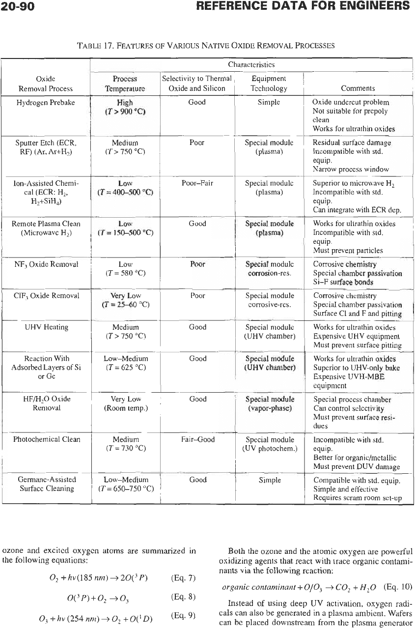
TABLE
17.
FEATURES
OF
VARIOUS
NATIVE
OXIDE
REMOVAL
PROCESSES
Characteristics
Oxide
Removal Process
Equipment
Technology
ielectivity
to
Thermal
Oxide and Silicon
Good
Process
Temperature
High
(T
>
900
"C)
Comments
Simple
Oxide undercut problem
Not suitable for prepoly
clean
Works for ultrathin oxides
Hydrogen Prebake
Sputter Etch (ECR,
RF)
(Ar,
Ar+H2)
Medium
(T
>
750
"C)
Poor
Special module
(plasma)
Residual surface damage
Incompatible with std.
equip.
Narrow process window
Low
(T
=
400-500 "C)
Poor-Fair Special module
(plasma)
Ion-Assisted Chemi-
cal (ECR: H,,
H,+SiH,)
Superior
to
microwave
H,
Incompatible with std.
equip.
Can integrate with ECR dep.
Works for ultrathin oxides
Incompatible with std.
equip.
Must prevent particles
Remote Plasma Clean
(Microwave H2)
Low
(T
=
150-500 "C)
Good
Special module
(plasma)
NF,
Oxide Removal
Low
(T
=
580 "C)
Poor Special module
corrosion-res.
Corrosive chemistry
Special chamber passivation
Si-F surface bonds
ClF, Oxide Removal Very Low
(T
=
2540
"C)
Poor Special module
corrosive-res.
Corrosive chemistry
Special chamber passivation
Surface CI and F and pitting
Works for ultrathin oxides
Expensive UHV equipment
Must prevent surface pitting
Works for ultrathin oxides
Superior
to
UHV-only bake
Expensive UVH-MBE
equipment
UHV Heating Medium
(T
>
750
"C)
Good Special module
(UHV chamber)
Reaction With
Adsorbed Layers of Si
or Ge
Low-Medium
(T
=
625 "C)
Good Special module
(UHV chamber)
HF/H,O Oxide
Removal
Very Low
(Room temp.)
Special process chamber
Can control selectivity
Must prevent surface resi-
dues
Photochemical Clean Special module
(UV photochem.)
Incompatible with std.
equip.
Better for organic/metallic
Must prevent DUV damage
Compatible with std. equip.
Simple and effective
Requires scram room set-up
Germane-Assisted
Surface Cleaning
Low-Medium Good
(T=650-75O0C)
ozone and excited oxygen atoms are summarized in
the following equations:
0,
+hv(185
nm)
+
20(3P)
Both the ozone and the atomic oxygen are powerful
oxidizing agents that react with trace organic contami-
nants via the
following
reaction:
organic contaminant
+
010,
-+
CO,
+
H,O
(Eq.
10)
Instead
of
using deep
UV
activation, oxygen radi-
cals can also be generated
in
a plasma ambient. Wafers
can be placed downstream from the plasma generator
(Eq.
7)
o(3
P)
+
0,
-+
0,
(Eq.
8)
0,
+
hv
(254
nm)
+
0,
+
O('D)
(Eq.
9,
INTEGRATED CIRCUITS
20-91
to minimize possible ion-induced damage. This well-
proven technique forms the basis of a number of com-
mercial photoresist ash reactors.
Metallic
Cleans-To keep the contaminants at or
accessibly close to the surface of the wafer and
because most metallic elements are fast diffusers at
moderately elevated temperatures, the chemistries cho-
sen for trace metallic removal must be able to form
volatile reaction products with
the
metallic contami-
nants without requiring too much thermal activation.
Various halogen-based techniques have been investi-
gated in this regard. Some success has been achieved
by photochemically activated chlorine chemistry.*
Since most chlorides of metals are not volatile at low
temperatures, it is believed that the cleaning action is
achieved by the slight etching
of
the silicon substrate
and that the metallic contaminants are "lifted
off'
the
surface of the wafer together with the volatile chlorides
of
silicon. As
in
the case
of
trace organic clean, chloride
chemistries based
on
plasma activation have also been
investigated and have achieved some degree of success.
Alternative nonhalogen-based Chemistries have also
been investigated by using a reactor with sources for
both the deep UV irradiation and the remote microwave
plasma activation.? Gases can be injected into the reac-
tor with or without the
W
or the plasma excitation.
The chemistries are chosen
so
that the reaction prod-
ucts are sufficiently volatile at relatively low tempera-
tures and
so
that the etching of exposed silicon can be
reduced to a minimum. The cleaning efficiencies of
these chemistries have been verified by using trace
amounts of radioactive isotopes of some of the most
commonly encountered contaminant elements (Fe, Cu,
etc.) plated onto bare silicon surfaces.
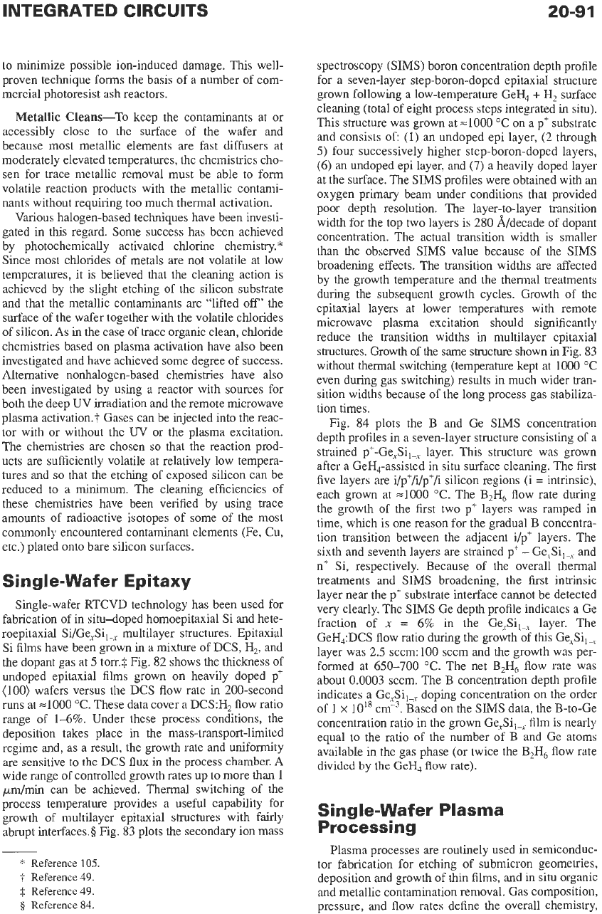
Single-Wafer Epitaxy
Single-wafer RTCVD technology has been used for
fabrication of in situ-doped homoepitaxial Si and hete-
roepitaxial Si/Ge,Si,, multilayer structures. Epitaxial
Si films have been grown
in
a mixture of DCS, H2, and
the dopant gas at
5
toaf Fig. 82 shows the thickness of
undoped epitaxial films grown
on
heavily doped p'
(100)
wafers versus the DCS flow rate in 200-second
runs
at
=lo00
"C. These data cover a DCS:H2 flow ratio
range
of
14%.
Under these process conditions,
the
deposition takes place in the mass-transport-limited
regime and, as a result, the growth rate and uniformity
are
sensitive to the
DCS
flux
in
the
process chamber. A
wide range
of
controlled growth rates up to more than
1
pm/min can be achieved. Thermal switching of the
process temperature provides a useful capability for
growth
of
multilayer epitaxial structures with fairly
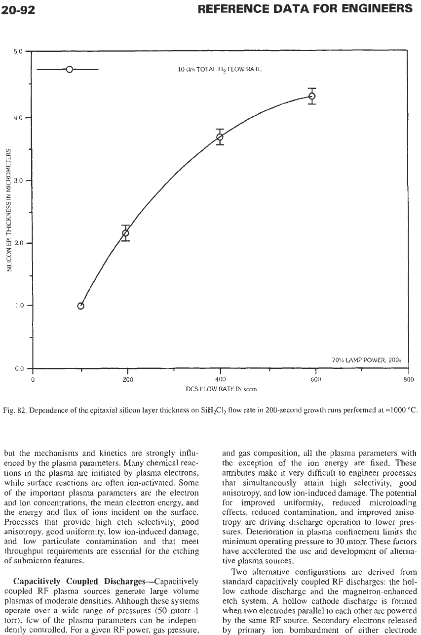
abrupt interfaces.§ Fig. 83 plots the secondary ion mass
*
Reference
105.
t
Reference
49.
$
Reference
49.
5
Reference
84.
spectroscopy
(SIMS)
boron concentration depth profile
for a seven-layer step-boron-doped epitaxial structure
grown following a low-temperature Ge%
+
H2 surface
cleaning (total
of
eight process steps integrated
in
situ).
This structure was grown at
=lo00
"C
on
a p+ substrate
and consists
of
(1)
an undoped epi layer, (2 through
5)
four successively higher step-boron-doped layers,
(6)
an undoped epi layer, and
(7)
a heavily doped layer
at the surface. The
SIMS
profiles were obtained with an
oxygen primary beam under conditions that provided
poor depth resolution. The layer-to-layer transition
width for the top two layers is 280 &decade of dopant
concentration. The actual transition width is smaller
than the observed SIMS value because
of
the SIMS
broadening effects. The transition widths are affected
by the growth temperature and the thermal treatments
during the subsequent growth cycles. Growth of the
epitaxial layers at lower temperatures with remote
microwave plasma excitation should significantly
reduce the transition widths in multilayer epitaxial
structures. Growth of the same structure shown in Fig. 83
without thermal switching (temperature kept at
1000
"C
even during gas switching) results in much wider tran-
sition widths because of the long process gas stabiliza-
tion
times.
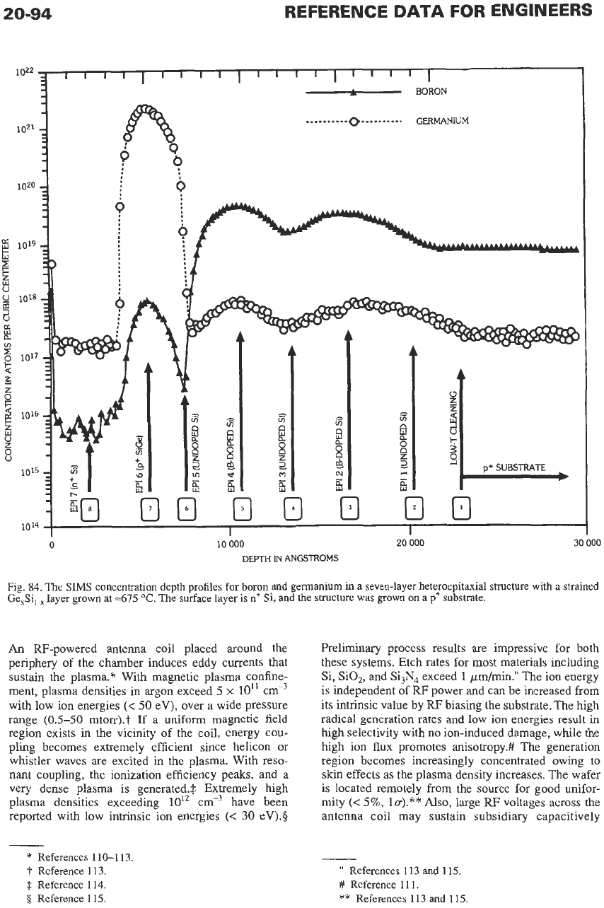
Fig. 84 plots the B and Ge SIMS concentration
depth profiles in a seven-layer structure consisting of a
strained p+-Ge,Si,-, layer. This structure was grown
after a GeH,-assisted in situ surface cleaning. The first
five layers are i/p+/i/p+/i silicon regions (i
=
intrinsic),
each grown at
=lo00
"C. The B2H, flow rate during
the growth of the first two p+ layers was ramped in
time, which is one reason for the gradual B concentra-
tion transition between the adjacent i/p' layers. The
sixth and seventh layers are strained p+
-
Ge,Si,, and
n+
Si, respectively. Because of the overall thermal
treatments and
SIMS
broadening, the first intrinsic
layer near the p+ substrate interface cannot be detected
very clearly. The SIMS Ge depth profile indicates a Ge
fraction of
x
=
6%
in the Ge,Si,, layer. The
GeH,:DCS flow ratio during the growth of
this
Ge,Si,,
layer was 2.5 sccm:
100
sccm and the growth was per-
formed at
650-700
"C. The net B2H, flow rate was
about
0.0003
sccm. The
B
concentration depth profile
indicates a Ge,Si,, doping concentration
on
the order
of
1
x
10"
~m-~. Based
on
the SIMS data, the B-to-Ge
concentration ratio in the grown Ge,Si,, film is nearly
equal to the ratio of the number of
B
and Ge atoms
available in the gas phase (or twice the B,H, flow rate
divided by the GeH, flow rate).
Single-Wafer Plasma
Processing
Plasma processes are routinely used
in
semiconduc-
tor fabrication
for
etching of submicron geometries,
deposition and growth of thin films, and in situ organic
and metallic contamination removal. Gas composition,
pressure, and flow rates define the overall chemistry,
20-92
REFERENCE
DATA
FOR ENGINEERS
5.0
4.0
0
B
t;
z
0
8
3.0
2
z
3
h
E
B
2.0
8
i
0
o_
1.0
10
slm
TOTAL
Hp
FLOW
RATE
70%
LAMP
POWER;
ZOOS
0.0
I
I
I I
0
200 400
DCS
FLOW RATE
IN
sccm
600
800
Fig.
82.
Dependence
of
the epitaxial silicon layer thickness
on SiH,Cl,
flow
rate
in
200-second growth
runs
performed at
=lo00
"C.
but the mechanisms and kinetics are strongly
influ-
enced by the plasma parameters. Many chemical reac-
tions in the plasma are initiated by plasma electrons,
while surface reactions are often ion-activated. Some
of
the important plasma parameters are the electron
and ion concentrations, the mean electron energy, and
the energy and flux of ions incident on the surface.
Processes that provide high etch selectivity, good
anisotropy, good uniformity, low ion-induced damage,
and low particulate contamination and that meet
throughput requirements are essential for the etching
of submicron features.
Capacitively Coupled Discharges-Capacitively
coupled RF plasma sources generate large volume
plasmas of moderate densities. Although these systems
operate over a wide range of pressures
(50
mtorr-1
torr), few
of
the plasma parameters can be indepen-
dently controlled. For
a
given
RF
power, gas pressure,
and gas composition, all the plasma parameters with
the exception of the ion energy are fixed. These
attributes make it very difficult to engineer processes
that simultaneously attain high selectivity, good
anisotropy, and low ion-induced damage. The potential
for improved uniformity, reduced microloading
effects, reduced contamination, and improved aniso-
tropy are driving discharge operation to lower pres-
sures. Deterioration in plasma confinement limits the
minimum operating pressure to
30
mtorr. These factors
have accelerated the use and development of altema-
tive plasma sources.
Two alternative configurations are derived from
standard capacitively coupled
RF
discharges: the hol-
low cathode discharge and the magnetron-enhanced
etch system.
A
hollow cathode discharge is formed
when two electrodes parallel to each other are powered
by the same
RF
source. Secondary electrons released
by primary ion bombardment of either electrode
INTEGRATED CIRCUITS
20-93
E
m
E
-
BORON
h
e
El
El
I
p+
SUBSTRATE
k
El
Fig. 83.
The
SIMS
boron concentration depth profile for
a
seven-layer epitaxial structure grown
at
=
1000
"C
with multiple rapid
switching of
the
wafer temperature following
a
low-temperature
GeH4+H2
pregrowth cleaning cycle.
bounce back and forth between the equipotential elec-
trodes, enhancing the ionization." This translates into
an enhanced plasma density, a large radical production
rate, and lower sheath voltages.? Impressive etch and
deposition results from hollow cathode systems have
been reported. For example, SiO, etch rates in excess
of
1
pm/min with selectivity to Si in excess of
50:l
and uniformities of
1%
have been reported.$
In
addi-
tion, hollow cathode systems are ideal for processes
involving simultaneous etch and deposition, either for
etch chemistries that rely
on
passivation through poly-
mer
on
side walls to achieve anisotropy and selectivity
or
in the deposition
of
planarized films.$ Sputtering
and deposition
on
the counter electrode and plasma
instability have prevented this discharge from gaining
wide acceptance, although methods for alleviating
some of these problems have been reported recently.§
*
Reference 106.
t
Reference 107.
$
Reference
108.
§
Reference
109.
The magnetron-enhanced RIE system employs
magnetic fields either parallel or perpendicular to the
surface of the powered electrode, to boost the ioniza-
tion efficiency and hence the plasma density. Since the
magnetic field reduces the electron mobility, discharge
operation can be extended to lower pressures
(<
30
mtorr), plasma confinement is improved, and the
sheath voltage decreases. The magnetron-enhanced
system is described more fully below. The hollow
cathode and magnetron systems provide good selectiv-
ity (because of the large radical flux and low ion ener-
gies), while the high ion flux ensures that anisotropy
is
not sacrificed. The
low
ion energies
also
imply reduced
ion-induced damage. Throughput is also enhanced.
Some of the limitations of capacitive coupling can-
not be overcome; sheath voltages increase with power.
The obvious
solution
is either to use inductive cou-
pling (inductively coupled RF discharges) or to use
higher frequencies (microwave discharges).
Inductively Coupled DischargesTwo generic
types of inductively coupled
RF
discharges have
evolved.
The
first is based purely
on
induction coupling.
20-94
REFERENCE
DATA
FOR
ENGINEERS
___t__
BORON
GERMANIUM
.........-o..........
0
10
000
20
000
DEPTH
IN ANGSTROMS
30
000
Fig.
84.
The
SIMS
concentration depth
profiles
for boron and germanium
in
a seven-layer heteroepitaxial structure with a strained
Ge,Si,~,
layer grown at
=675
"C.
The
surface layer
is
n+
Si,
and the structure was grown
on
a p+ substrate.
An
RF-powered antenna coil placed around the
periphery of the chamber induces eddy currents that
sustain the plasma.* With magnetic plasma confine-
ment, plasma densities in argon exceed
5
x
10"
cm-3
with low ion energies
(<
50
eV), over
a
wide pressure
range
(0.5-50
mtorr).?
If
a
uniform
magnetic field
region exists in the vicinity of the coil, energy cou-
pling becomes extremely efficient since helicon or
whistler waves are excited in the plasma. With reso-
nant coupling, the ionization efficiency peaks, and
a
very dense plasma is generated.$ Extremely high
plasma densities exceeding
10"
cm-3 have been
reported with low intrinsic ion energies
(i
30
eV).§
Preliminary process results are impressive for both
these systems. Etch rates for most materials including
Si, SiO,, and Si3N, exceed
1
pm/min." The ion energy
is independent of
RF
power and can be increased from
its intrinsic value by
RF
biasing the substrate. The high
radical generation rates and
low
ion
energies result
in
high selectivity with no ion-induced damage, while the
high ion flux promotes anisotropy.# The generation
region becomes increasingly concentrated owing
to
skin effects
as
the plasma density increases. The wafer
is located remotely from the source for good unifor-
mity
(<
5%,
1g).**
Also, large
RF
voltages across the
antenna coil may sustain subsidiary capacitively
*
References 110-1
13.
T
Reference 113.
$
Reference 114.
§
Reference 115.
"
References 113 and 115.
#
Reference
11 1.
**
References 113 and 115
INTEGRATED CIRCUITS
20-95
coupled discharges that cause sputter damage of the
chamber walls and possible contamination.
Magnetron-Enhanced DischargesMagnetron
effects induced by external magnetic fields extend dis-
charge operation to lower pressures. Electron mobility
along
a
direction perpendicular to the magnetic field is
reduced by the factor"
where
0,
is the electron cyclotron frequency,
v,,
is the electron momentum transfer collision fre-
The reduced electron mobility produces better plasma
confinement and a reduction in sheath voltages.
In
addition, the ionization efficiency of secondary elec-
trons emitted from the powered electrodes is
enhanced. Both these effects lead to an increase in the
plasma density.
A
factor of
10
enhancement in plasma
density is possible with moderate fields
(=
250
G).t
Because of the significant dissociation, the plasma
chemistry can differ between RE and magnetron-
enhanced systems.$
Various configurations have been investigated. Mag-
netron systems have traditionally been used for sput-
tering applications, where discharge operation at
submilliton: pressures is vital. The most common con-
figurations include the planar magnetron discharge,
with the magnetic field perpendicular to the electric
field, and cylindrical magnetron discharges. The mag-
netic field is generated by permanent magnets or elec-
tromagnets located behind the powered electrode.
Typically the magnetic field is oriented
so
that the
E
x
B
electron drift forms
a
closed loop, thereby trapping the
electrons in the vicinity of the electrode.§
In
the con-
ventional planar magnetron, a disk magnet surrounded
by
a
ring magnet produces radial magnetic fields. The
magnetic field parallel to the wafer is most intense at
midradius. Plasma nonuniformity is a big concern in
these systems. Because the plasma is most intense in
regions where the magnetic field component parallel to
the wafer is a maximum, it causes a race track etch
characterized by a fast etch at midradius.9 While this
configuration results in
E
X
B
drift currents that form
a
closed loop, the severe nonuniformity" has prompted
the use of alternative magnetic field patterns. One of
the options is
to
keep the magnetic
field
lines parallel
to each other and to the electrode.
To
counter the effect
of the asymmetric
E
x
B
drift, the magnets or wafer
can be rotated or scanned.#
quency.
*
Reference
116.
t
Reference 117.
$
Reference
118.
8
Reference
119.
"
Reference
120.
#
Reference 121.
An
adjustable field planar magnetron discharge has
been reported.** Rare-earth permanent magnets
located behind the wafer induce
a
magnetic field paral-
lel to the wafer surface.
Also,
the field lines
are
parallel
to each other in
the
region of the wafer. The magnet
lengths are scaled
so
as to achieve a uniform magnetic
field over the wafer. Movable soft-iron slugs can be
used to tailor the magnetic field distribution further.
The slugs are located between the magnets and behind
the
powered electrode. The magnetic field at the wafer
is
=
500
G. The magnetron
RE
system is otherwise
similar to
a
parallel plate system.
In
addition to power-
ing the electrode, a cylindrical ring around the counter
electrode can also be powered with a low-frequency or
high-frequency RF power supply. Grounding or
RF
biasing the ring can be used to optimize uniformity
and vary the energy of ions incident
on
the substrate.
In
addition, a contoured counterelectrode further
improves the etch uniformity. For ion-assisted pro-
cesses there is an optimum field strength. For very
strong fields, the ion energy is too low, and the etch is
hindered.tt However, the plasma density increases
with increasing field strength. The cylindrical ring per-
mits operation with strong fields without the attendant
reduction
in
etch rate. By manipulating the slugs and
the ring, the location of fastest etch can be moved pro-
gressively from the wafer center to
the
wafer edge.
This flexibility may be exploited to compensate for
nonuniformities resulting from previous process steps.
This
magnetron RE system has been specifically
optimized for DESIRE, a
dry
develop lithography pro-
cess. The basic steps involved in DESIRE are as fol-
lows. Exposed photoresist is exposed to
a
silylating
agent such
as
HMDS
(hexa methyl disilane). This
causes silicon
to
be incorporated in the resist. The
depth of silicon incorporation is
a
function of exposure
dose. When this resist is exposed
to
an
0,
plasma, the
silicon in the photoresist is converted to SiO,.
Ion
bombardment continuously sputters
the
SiO.,
as
it is
formed. Ultimately the sputter etch depth in the unex-
posed (or marginally exposed) regions exceeds the
depth of silicon incorporation,
and
no
further Si0 for-
mation occurs. The etch now proceeds rapidly as the
photoresist is consumed by the
0,
plasma.
In
the
strongly exposed regions, the SiO, that is continually
formed forms the etch mask that hinders the etch.
The nature of this process places very stringent
demands
on
the capabilities of the etch process. The
ion energy has to be sufficiently low for reasonable
etch selectivity between
SiO,
and
the photoresist.
At
the same time, a very high etch selectivity exaggerates
etch nonuniformities and promotes residue formation.
Selectivities between 5:l and 8:l are ideal. Since the
silylation depth does not exhibit any strong threshold-
ing behavior with respect to exposure, the budget for
etch nonuniformities
is
very small. The requirements
**
Reference 49.
tt
Reference 117
20-96
REFERENCE
DATA
FOR
ENGINEERS
become especially tight for contact patterns. To engi-
neer an acceptable process, the resist etch and Si0
sputter etch uniformity have to be within
4%
(1~).
Finally, vertical etch profiles with
no
undercut require
high anisotropy. Undercut can be eliminated by reduc-
ing the
0,
flow and cooling the wafer to below
-35
"C.
These requirements of good selectivity and high
anisotropy uniformity preclude the use of an RE etch
system. The magnetron-enhanced RE system with
adjustable magnetic fields and ion energies appears to
be a good choice. Good results have been reported for
0.4
pm
lines and spaces processed using such a sys-
tem.* Nominal process conditions were
115
W,
3
mtorr,
40
sccm
O,,
and a DC bias of
-85
V. A similar
system may be used for implementing other etch pro-
cesses that are also tightly constrained.
Microwave Discharges-Microwave discharges
have almost become synonymous with electron cyclo-
tron resonance (ECR) discharges. However, cavity
based microwave discharges still maintain their niche
for afterglow plasmas. A remote microwave plasma is
a copious source of radicals and is generally used in
conjunction with a capacitively coupled plasma to
enhance the etch or deposition rates.
ECR discharges
are
a source of large volume dense
plasmas. At the resonance condition that occurs for a
magnetic field of
875
G for
2.45
GHz microwave exci-
tation, the power coupling becomes resonant. At reso-
nance, the electron cyclotron frequency and the
microwave frequencies are synchronized,
so
that elec-
trons are continuously accelerated by the electric field.
ECR
is
most effective for pressures between
lo-'
and
10
mtorr, when an electron can undergo several orbits
before suffering a scattering collision. Typical plasma
densities exceed
10"
~m-~, with ion current densities
to the wafer in excess of
IO
mA/cm2.t At the same
time, the intrinsic ion energy is fairly low
(i
30
eV),
which can be increased by
RF
biasing the wafer. Even
in the absence
of
cyclotron resonance, magnetized
plasmas can still couple microwave power. However,
the mean electron energy and consequently the ioniza-
tion
efficiency is much lower. For a given input power,
the
higher the ionization efficiency, the higher is the
plasma density. Thus the size and coupling efficiency
of the ECR region can dramatically affect the plasma
density for
a
given input power.$ Still, magnetized
microwave plasmas generate high plasma densities
compared to capacitively coupled discharges.
ECR plasmas offer tremendous process flexibility.
High-quality etching of a range
of
materials including
Si,§ SiO,," Al," resist,# and 111-V materials** is possi-
*
Reference 49.
t
Reference 122.
$
Reference
123.
5
Reference 124.
"
Reference
125.
#
Reference
126.
**
Reference 127.
ble. Similarly, deposition processes can also be accom-
plished at comparatively low temperatures.??
Various types of ECR sources have been devel-
oped.$$ Perhaps
the
most common source uses a set of
electromagnets around the discharge chamber that
generate axial magnetic fields.§§ A divergent or
mirror
magnetic field configuration can be attained with
appropriate solenoid and pole-piece configurations.
The axial magnetic field is tailored
so
that it is a maxi-
mum at the microwave input end and decreases toward
the wafer. The microwave coupler launches the right-
hand circularly polarized wave, which couples very
efficiently into the plasma, generating a dense
plasma."" The ECR region is fairly large since the
axial magnetic field is quite uniform in the radial
direction and decreases away from the microwave cou-
pler. The axial magnetic field also enhances the ion
current density at the wafer but may degrade unifor-
mity and directionality of ions.## Remote wafer loca-
tion is required for good uniformity. However, placing
the wafer too far away reduces the radical
flux
and
affects throughput. A third electromagnet in the pro-
cess chamber can be used to mitigate some of these
trade-offs.*
* *
Another option is to use a set
of
permanent magnets
that generate a multipolar cusp field around the periph-
ery of the discharge chamber.??? The ECR region is
then a thin shell around the inside of the plasma forma-
tion chamber. Because the plasma formation regions
are much closer to the wall, and the size of the ECR
region is limited, the attainable plasma densities
appear to be lower. Since the plasma diffuses freely
from the chamber toward the wafer, good uniformity
can be attained much closer to
the
source.?tt
The last option
is
to combine the plasma formation
chamber with the process chamber as in the distributed
ECR design (DECR).S$$ Permanent magnets establish
a multipolar cusp field around the periphery
of
the pro-
cess chamber. Multiple microwave antennas are placed
around the periphery of the chamber. The ECR region
once again is a thin shell around the inside of the pro-
cess chamber. The plasma diffuses radially toward the
wafer, which is located centrally in a field-free region.
However, the plasma densities reported for such a
source are a factor of five lower than those obtained
with other sources. The discharge behaves more like a
magnetized microwave plasma, with resonant power
coupling occurring in a very small region.
It
References
126,
128,
and
129.
$$
Reference 122.
53
Reference
130.
""
Reference 123.
##
Reference 131.
***
Reference
132.
ttt
Reference
133.
$$$
Reference
134.
INTEGRATED
CIRCUITS
II
I
I
I
I
I
I
Ill
I
I
Ill
I
I
20-97
A
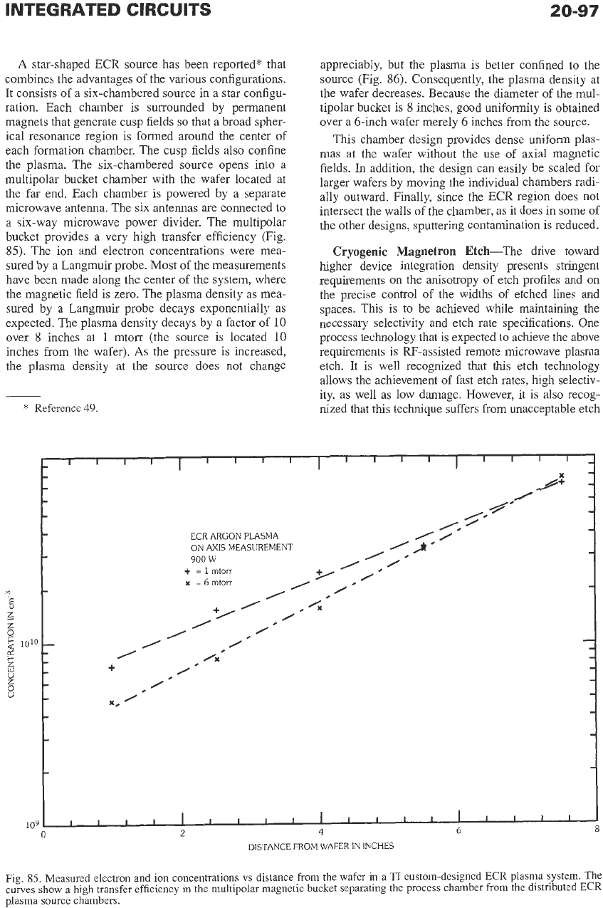
star-shaped ECR source has been reported* that
combines the advantages of the various configurations.
It consists of a six-chambered source in
a
star configu-
ration. Each chamber is surrounded by permanent
magnets that generate cusp fields
so
that
a
broad spher-
ical resonance region is formed around the center of
each formation chamber. The cusp fields also confine
the plasma. The six-chambered source opens into a
multipolar bucket chamber with the wafer located at
the
far end. Each chamber is powered by
a
separate
microwave antenna. The six antennas are connected to
a
six-way microwave power divider. The multipolar
bucket provides
a
very high transfer efficiency (Fig.
85).
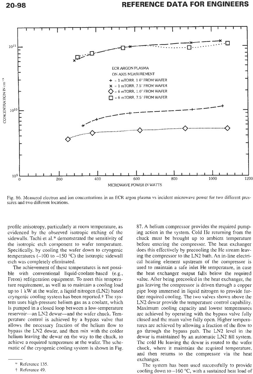
The ion and electron concentrations were mea-
sured by a Langmuir probe. Most of the measurements
have been made along the center of the system, where
the magnetic field is zero. The plasma density
as
mea-
sured by
a
Langmuir probe decays exponentially
as
expected. The plasma density decays by
a
factor of
10
over
8
inches
at
1
mtorr (the source is located
10
inches from the wafer).
As
the pressure is increased,
the plasma density at the source does
not
change
*
Reference
49.
appreciably, but the plasma is better confined to the
source (Fig. 86). Consequently, the plasma density at
the wafer decreases. Because the diameter of the mul-
tipolar bucket is
8
inches, good uniformity is obtained
over a 6-inch wafer merely 6 inches from the source.
This chamber design provides dense uniform plas-
mas at the wafer without the use
of
axial magnetic
fields.
In
addition, the design can easily be scaled for
larger wafers by moving the individual chambers radi-
ally outward. Finally, since the ECR region does not
intersect the walls
of
the chamber,
as
it does in some
of
the other designs, sputtering contamination is reduced.
Cryogenic Magnetron Etch-The drive toward
higher device integration density presents stringent
requirements
on
the
anisotropy of etch profiles and
on
the precise control of the widths of etched lines and
spaces. This is to be achieved while maintaining the
necessary selectivity and etch rate specifications. One
process technology that is expected
to
achieve the above
requirements is RF-assisted remote microwave plasma
etch. It is well recognized that this etch technology
allows the achievement of fast etch rates, high selectiv-
ity,
as
well
as
low damage. However, it is also recog-
nized that
this
technique suffers from unacceptable etch
I
I
I'
I
I1
I
Ill
I
I
I I
.+'
ECR ARGON PLASMA
ON
AXIS
MEASUREMENT
900
W
f,/
+
=
1
mtorr
x
=
6
mtorr
0
m
/
0
'E,
0
/X-
20-98
REFERENCE
DATA
FOR ENGINEERS
- -
-
--
-
5.
.o
/.e+----
..............
0.
.......
ECR ARGON PLASMA
ON
AXIS
MEASUREMENT
+
=
1
mTORR,
1.0
FROM WAFER
X
=
1
rnTORR,
7.5"
FROM WAFER
0
=
6
mTORR,
1.0
FROM WAFER
0
=
6
mTORR.
7.5"
FROM WAFER
-~
_------
--+----.*
.........
0
...........................
0
........................
0
200
400
600
800
1000
1200
MICROWAVE POWER
IN
WATTS
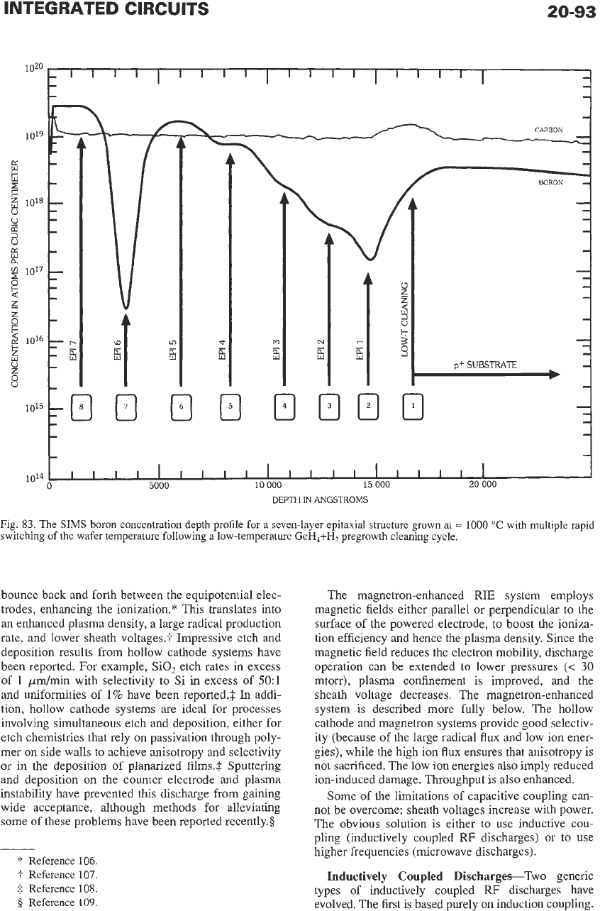
Fig.
86.
Measured electron and ion concentrations in
an
ECR
argon plasma
vs
incident microwave power for two different pres-
sures and
two
different locations.
profile anisotropy, particularly at room temperature,
as
evidenced by the observed isotropic etching of the
sidewalls. Tachi et al.* demonstrated the sensitivity
of
the isotropic etch component to wafer temperature.
Specifically, by cooling the wafer down to cryogenic
temperatures
(-100
to
-150
"C) the isotropic sidewall
etch was completely eliminated.
The achievement
of
these temperatures is not possi-
ble with conventional liquid-coolant-based (e.g.,
Freon) refrigeration equipment. To meet this tempera-
ture requirement,
as
well
as
to maintain
a
cooling load
up
to
1
kW
at the wafer,
a
liquid nitrogen
(LN2)
based
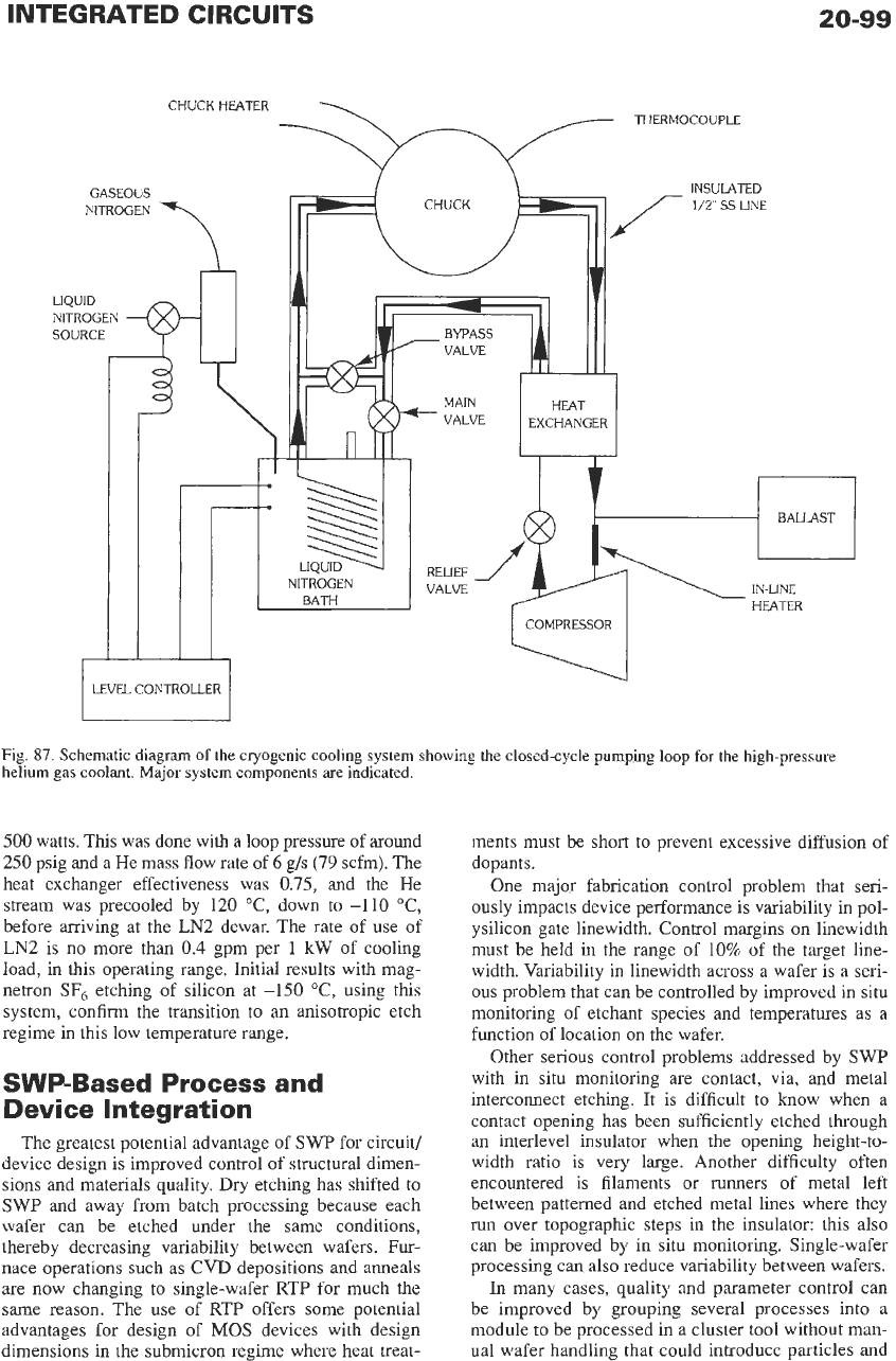
cryogenic cooling system has been reported.? The sys-
tem uses high-pressure helium gas as
a
coolant, which
is pumped in
a
closed loop between
a
low-temperature
reservoir-an
LN2
dewar-and the wafer chuck. Tem-
perature control
is
achieved by a bypass valve that
allows the necessary fraction of the helium flow to
bypass the
LN2
dewar, and then mix with the colder
helium leaving the dewar on the way to the chuck,
to
achieve
a
required temperature at the wafer. The sche-
matic of the cryogenic cooling system is shown in Fig.
*
Reference
135.
t
Reference
49.
87.
A
helium compressor provides the required pump-
ing action in the system. Cold He returning from the
chuck must be brought up to ambient temperature
before entering the compressor. The heat exchanger
does this effectively by precooling the He stream leav-
ing the compressor to the
LN2
bath. An in-line electri-
cal heating element upstream
of
the compressor is
used to maintain
a
safe inlet He temperature, in case
the heat exchanger output falls below the required
value. After being precooled in the heat exchanger, the
gas leaving the compressor is driven through
a
copper
pipe loop immersed in liquid nitrogen
to
provide fur-
ther required cooling. The two valves shown above the
LN2
dewar provide the temperature control capability.
Maximum cooling capacity and lowest temperatures
are achieved by operating with the bypass valve fully
closed and the main valve fully open. Higher tempera-
tures are achieved by allowing
a
fraction of the flow to
go through the bypass path. The
LN2
level in the
dewar is maintained by an automatic
LN2
fill
system.
The cold He leaving the dewar is routed to the wafer
chuck, where it maintains the required temperature,
and then returns to the compressor via the heat
exchanger.
The system has been used successfully to provide
cooling down to
-160
"C, with a sustained heat load of
INTEGRATED CIRCUITS
20-99
r
-4
COMPRESSOR
i_____
LEVEL CONTROLLER
Fig.
87.
Schematic diagram
of
the cryogenic cooling system showing the closed-cycle pumping loop for the high-pressure
helium gas coolant. Major system components
are
indicated.
500
watts.
This
was done with a loop pressure of around
250
psig and a He mass flow rate of
6
g/s
(79
scfm). The
heat exchanger effectiveness was
0.75,
and the He
stream was precooled by 120 "C, down to -110
"C,
before arriving at the
LN2
dewar. The rate of use of
LN2
is
no
more than
0.4
gpm per
1
kW
of cooling
load, in this operating range. Initial results with mag-
netron
SF,
etching of silicon at -150
"C,
using this
system, confirm the transition to an anisotropic etch
regime in this low temperature range.
SWP-Based Process and
Device
Integration
The greatest potential advantage of
SWP
for circuit/
device design is improved control of structural dimen-
sions and materials quality. Dry etching has shifted to
SWP
and away from batch processing because each
wafer can be etched under the same conditions,
thereby decreasing variability between wafers.
Fur-
nace operations such as CVD depositions and anneals
are now changing to single-wafer RTP for much the
same reason. The use of RTP offers some potential
advantages for design of
MOS
devices with design
dimensions
in
the submicron regime where heat treat-
ments must be short to prevent excessive diffusion of
dopants.
One major fabrication control problem that seri-
ously impacts device performance is variability in pol-
ysilicon gate linewidth. Control margins on linewidth
must be held in the range of
10%
of the target line-
width. Variability in linewidth across a wafer is a seri-
ous problem that can be controlled by improved in situ
monitoring of etchant species and temperatures as a
function of location on the wafer.
Other serious control problems addressed by
SWP
with in situ monitoring are contact, via, and metal
interconnect etching. It
is
difficult to know when
a
contact opening has been sufficiently etched through
an interlevel insulator when the opening height-to-
width ratio is very large. Another difficulty often
encountered is filaments or runners of metal left
between patterned and etched metal lines where they
run over topographic steps
in
the insulator: this also
can be improved by in situ monitoring. Single-wafer
processing can also reduce variability between wafers.
In
many cases, quality and parameter control can
be improved by grouping several processes into
a
module to be processed in a cluster
tool
without man-
ual wafer handling that could introduce particles and