Neamen D. Microelectronics: Circuit Analysis and Design
Подождите немного. Документ загружается.

68 Part 1 Semiconductor Devices and Basic Applications
+
–
Diode
rectifier
Voltage
regulator
Filter
AC
voltage
source
Power
transformer
LOAD
v
O
+
_
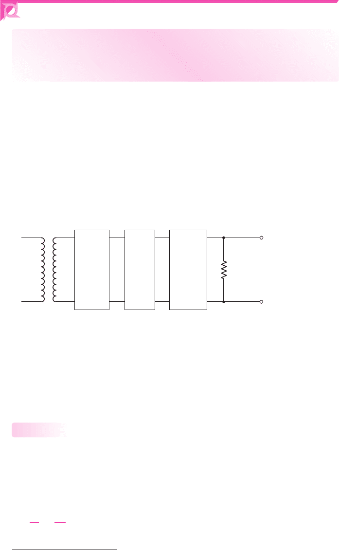
Figure 2.1 Diagram of an electronic power supply. The circuits that characterize each block
diagram are considered in this chapter.
1
Ideally, the output voltage of a rectifier circuit is a dc voltage. However, as we will see, there may be an
ac ripple voltage superimposed on a dc value. For this reason, we will use the notation
v
O
as the instanta-
neous value of output voltage.
2.1 RECTIFIER CIRCUITS
Objective: • Determine the operation and characteristics of diode
rectifier circuits, which form the first stage in the process of converting
an ac signal into a dc signal in the electronic power supply.
One application of diodes is in the design of rectifier circuits. A diode rectifier forms the
first stage of a dc power supply. A dc voltage is required to power essentially every elec-
tronic device, including personal computers, televisions, and stereo systems. An electri-
cal cord that is plugged into a wall socket and attached to a television, for example, is
connected to a rectifier circuit inside the TV. In addition, battery chargers for portable
electronic devices such as cell phones and laptop computers contain rectifier circuits.
Figure 2.1 is a diagram of a dc power supply. The output voltage
1
v
O
is usually
in the range of 3 to 24 V depending on the particular electronics application.
Throughout the first part of this chapter, we will analyze and design various stages in
the power supply circuit.
Rectification is the process of converting an alternating (ac) voltage into one that
is limited to one polarity. The diode is useful for this function because of its nonlin-
ear characteristics, that is, current exists for one voltage polarity, but is essentially
zero for the opposite polarity. Rectification is classified as half-wave or full-wave,
with half-wave being the simpler and full-wave being more efficient.
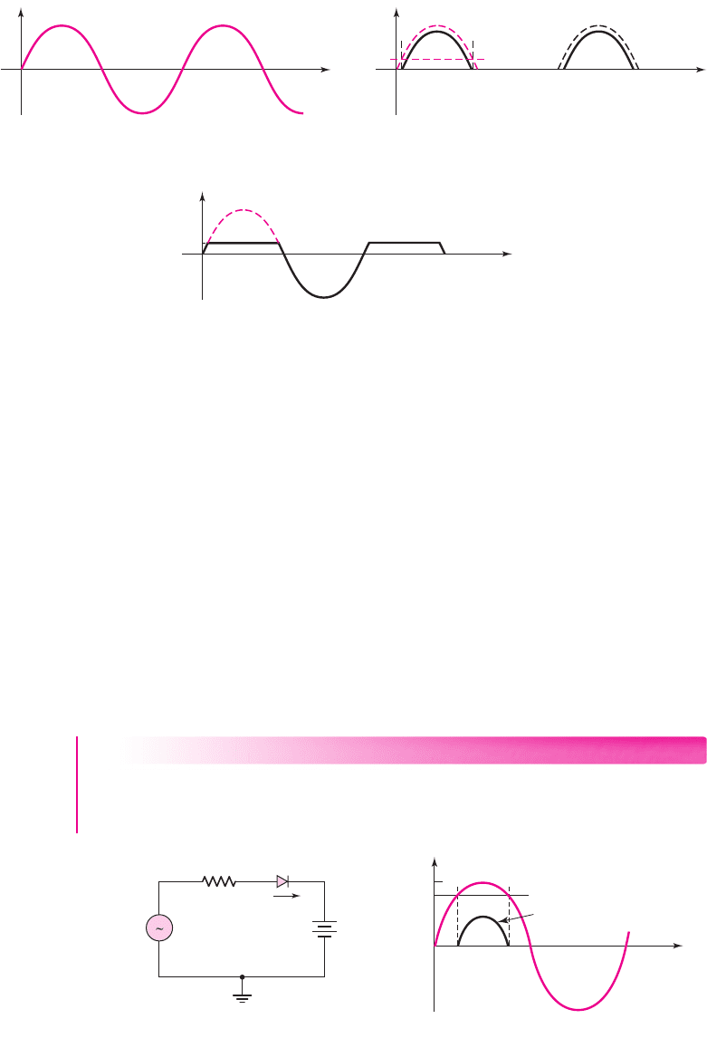
Half-Wave Rectification
Figure 2.2(a) shows a power transformer with a diode and resistor connected to the
secondary of the transformer. We will use the piecewise linear approach in analyzing
this circuit, assuming the diode forward resistance is
r
f
= 0
when the diode is “on.”
The input signal,
v
I
, is, in general, a 120 V (rms), 60 Hz ac signal. Recall that the
secondary voltage,
v
S
, and primary voltage,
v
I
, of an ideal transformer are related by
v
I
v
S
=
N
1
N
2
(2.1)
2.1.1
nea80644_ch02_067-124.qxd 06/08/2009 07:28 PM Page 68 F506 Tempwork:Dont' Del Rakesh:June:Rakesh 06-08-09:MHDQ134-02 Folder:M

Chapter 2 Diode Circuits 69
(a) (b)
v
S
0
Slope = 1
V
g
v
O
v
I
v
S
v
O
+
+
–
–
+
–
R
N
1
N
2
Figure 2.2 Half-wave rectifier (a) circuit and (b) voltage transfer characteristics
where
N
1
and
N
2
are the number of primary and secondary turns, respectively. The
ratio
N
1
/N
2
is called the transformer turns ratio. The transformer turns ratio will
be designed to provide a particular secondary voltage,
v
S
, which in turn will produce
a particular output voltage
v
O
.
Problem-Solving Technique: Diode Circuits
In using the piecewise linear model of the diode, the first objective is to determine
the linear region (conducting or not conducting) in which the diode is operating.
To do this, we can:
1. Determine the input voltage condition such that a diode is conducting (on).
Then find the output signal for this condition.
2. Determine the input voltage condition such that a diode is not conducting
(off). Then find the output signal for this condition.
[Note: Item 2 can be performed before item 1 if desired.]
Figure 2.2(b) shows the voltage transfer characteristics,
v
O
versus
v
S
, for the
circuit. For
v
S
< 0
, the diode is reverse biased, which means that the current is zero
and the output voltage is zero. As long as
v
S
< V
γ
, the diode will be nonconducting,
so the output voltage will remain zero. When
v
S
> V
γ
,
the diode becomes forward
biased and a current is induced in the circuit. In this case, we can write
i
D
=
v
S
− V
γ
R
(2.2(a))
and
v
O
= i
D
R = v
S
− V
γ
(2.2(b))
For
v
S
> V
γ
, the slope of the transfer curve is 1.
If
v
S
is a sinusoidal signal, as shown in Figure 2.3(a), the output voltage can be
found using the voltage transfer curve in Figure 2.2(b). For
v
S
≤ V
γ
the output volt-
age is zero; for
v
S
> V
γ
, the output is given by Equation (2.2(b)), or
v
O
= v
S
− V
γ
and is shown in Figure 2.3(b). We can see that while the input signal
v
S
alternates
polarity and has a time-average value of zero, the output voltage
v
O
is unidirectional
and has an average value that is not zero. The input signal is therefore rectified. Also,
since the output voltage appears only during the positive cycle of the input signal, the
circuit is called a half-wave rectifier.
nea80644_ch02_067-124.qxd 06/08/2009 07:28 PM Page 69 F506 Tempwork:Dont' Del Rakesh:June:Rakesh 06-08-09:MHDQ134-02 Folder:M
70 Part 1 Semiconductor Devices and Basic Applications
v
S
v
S
v
S
t
0
v
v
O
t
V
g
v
D
V
g
v
t
(a) (b)
(c)
Figure 2.3 Signals of the half-wave rectifier circuit: (a) sinusoidal input voltage, (b) rectified
output voltage, and (c) diode voltage
+
–
i
D
V
B
R
v
S
(t) =
V
S
sin wt
v
S
(t)
V
S
V
B
+ V
g
+
–
wt
wt
1
wt
2
(a) (b)
i
D
(t)
Figure 2.4 (a) Half-wave rectifier used as a battery charger; (b) input voltage and diode
current waveforms
When the diode is cut off and nonconducting, no voltage drop occurs across
the resistor R; therefore, the entire input signal voltage appears across the diode
(Figure 2.3(c)). Consequently, the diode must be capable of handling the peak
current in the forward direction and sustaining the largest peak inverse voltage (PIV)
without breakdown. For the circuit shown in Figure 2.2(a), the value of PIV is equal
to the peak value of
v
S
.
We can use a half-wave rectifier circuit to charge a battery as shown in Figure 2.4(a).
Charging current exists whenever the instantaneous ac source voltage is greater than
the battery voltage plus the diode cut-in voltage as shown in Figure 2.4(b). The resis-
tance R in the circuit is to limit the current. When the ac source voltage is less than
V
B
,
the current is zero. Thus current flows only in the direction to charge the battery. One
disadvantage of the half-wave rectifier is that we “waste” the negative half-cycles. The
current is zero during the negative half-cycles, so there is no energy dissipated, but at
the same time, we are not making use of any possible available energy.
EXAMPLE 2.1
Objective: Determine the currents and voltages in a half-wave rectifier circuit.
Consider the circuit shown in Figure 2.4. Assume
V
B
= 12
V,
R = 100
, and
V
γ
= 0.6
V. Also assume
v
S
(t) = 24 sin ωt.
Determine the peak diode current,
nea80644_ch02_067-124.qxd 06/08/2009 07:28 PM Page 70 F506 Tempwork:Dont' Del Rakesh:June:Rakesh 06-08-09:MHDQ134-02 Folder:M

Chapter 2 Diode Circuits 71
maximum reverse-bias diode voltage, and the fraction of the cycle over which the
diode is conducting.
Solution: Peak diode current:
i
D
(peak) =
V
S
− V
B
− V
γ
R
=
24 − 12 −0.6
0.10
= 114 mA
Maximum reverse-bias diode voltage:
v
R
(max) = V
S
+ V
B
= 24 +12 = 36 V
Diode conduction cycle:
v
I
= 24 sin ωt
1
= 12.6
or
ωt
1
= sin
−1
12.6
24
⇒ 31.7
◦
By symmetry,
ωt
2
= 180 −31.7 = 148.3
◦
Then
Percent time =
148.3 − 31.7
360
×100% = 32.4%
Comment: This example shows that the diode conducts only approximately one-
third of the time, which means that the efficiency of this battery charger is quite low.
EXERCISE PROBLEM
Ex 2.1: Repeat Example 2.1 if the input voltage is
v
s
(t) = 12 sin ωt
(V),
V
B
= 4.5
V, and
R = 250
. (Ans.
i
D
(peak) = 27.6
mA,
v
R
(max) = 16.5
V,
36.0 %)
Full-Wave Rectification
The full-wave rectifier inverts the negative portions of the sine wave so that a unipo-
lar output signal is generated during both halves of the input sinusoid. One example
of a full-wave rectifier circuit appears in Figure 2.5(a). The input to the rectifier con-
sists of a power transformer, in which the input is normally a 120 V (rms), 60 Hz ac
signal, and the two outputs are from a center-tapped secondary winding that provides
equal voltages
v
S
, with the polarities shown. When the input line voltage is positive,
both output signal voltages
v
S
are also positive.
The primary winding connected to the 120 V ac source has
N
1
windings, and
each half of the secondary winding has
N
2
windings. The value of the
v
S
output volt-
age is
120 (N
2
/N
1
)
volts (rms). The turns ratio of the transformer, usually desig-
nated
(N
1
/N
2
)
can be designed to “step down” the input line voltage to a value that
will produce a particular dc output voltage from the rectifier.
The input power transformer also provides electrical isolation between the pow-
erline circuit and the electronic circuits to be biased by the rectifier circuit. This iso-
lation reduces the risk of electrical shock.
2.1.2
nea80644_ch02_067-124.qxd 06/08/2009 07:28 PM Page 71 F506 Tempwork:Dont' Del Rakesh:June:Rakesh 06-08-09:MHDQ134-02 Folder:M
72 Part 1 Semiconductor Devices and Basic Applications
During the positive half of the input voltage cycle, both output voltages
v
S
are
positive; therefore, diode
D
1
is forward biased and conducting and
D
2
is reverse
biased and cut off. The current through
D
1
and the output resistance produce a posi-
tive output voltage. During the negative half cycle,
D
1
is cut off and
D
2
is forward
biased, or “on,” and the current through the output resistance again produces a posi-
tive output voltage. If we assume that the forward diode resistance
r
f
of each diode
is small and negligible, we obtain the voltage transfer characteristics,
v
O
versus
v
S
,
shown in Figure 2.5(b).
For a sinusoidal input voltage, we can determine the output voltage versus time
by using the voltage transfer curve shown in Figure 2.5(b). When
v
S
> V
γ
, D
1
is on
and the output voltage is
v
O
= v
S
− V
γ
. When
v
S
is negative, then for
v
S
< −V
γ
or
−v
S
> V
γ
, D
2
is on and the output voltage is
v
O
=−v
S
− V
γ
. The corresponding
input and output voltage signals are shown in Figure 2.5(c). Since a rectified output
voltage occurs during both the positive and negative cycles of the input signal, this
circuit is called a full-wave rectifier.
Another example of a full-wave rectifier circuit appears in Figure 2.6(a). This cir-
cuit is a bridge rectifier, which still provides electrical isolation between the input ac
powerline and the rectifier output, but does not require a center-tapped secondary wind-
ing. However, it does use four diodes, compared to only two in the previous circuit.
During the positive half of the input voltage cycle,
v
S
is positive,
D
1
and
D
2
are
forward biased,
D
3
and
D
4
are reverse biased, and the direction of the current is as
shown in Figure 2.6(a). During the negative half-cycle of the input voltage,
v
S
is neg-
ative, and
D
3
and
D
4
are forward biased. The direction of the current, shown in
Figure 2.6(b), produces the same output voltage polarity as before.
Figure 2.6(c) shows the sinusoidal voltage
v
S
and the rectified output voltage
v
O
. Because two diodes are in series in the conduction path, the magnitude of
v
O
is
two diode drops less than the magnitude of
v
S
.
One difference to be noted in the bridge rectifier circuit in Figure 2.6(a) and the
rectifier in Figure 2.5(a) is the ground connection. Whereas the center tap of the
secondary winding of the circuit in Figure 2.5(a) is at ground potential, the secondary
+
–
v
I
D
1
D
2
R
+
–
v
O
+
–
v
S
+
–
v
S
–V
g
v
O
v
S
V
g
0
Slope –
∼
–1 Slope –
∼
1
v
v
S
–v
S
v
O
D
1
on D
2
on D
1
on D
1
onD
2
on
t
V
g
T 2T
T
2
3T
2
(b)(a)
(c)
Figure 2.5 Full-wave rectifier: (a) circuit with center-tapped transformer, (b) voltage transfer
characteristics, and (c) input and output waveforms
nea80644_ch02_067-124.qxd 06/08/2009 07:28 PM Page 72 F506 Tempwork:Dont' Del Rakesh:June:Rakesh 06-08-09:MHDQ134-02 Folder:M

Chapter 2 Diode Circuits 73
winding of the bridge circuit (Figure 2.6(a)) is not directly grounded. One side of the
load R is grounded, but the secondary of the transformer is not.
EXAMPLE 2.2
Objective: Compare voltages and the transformer turns ratio in two full-wave recti-
fier circuits.
Consider the rectifier circuits shown in Figures 2.5(a) and 2.6(a). Assume the
input voltage is from a 120 V (rms), 60 Hz ac source. The desired peak output volt-
age
v
O
is 9 V, and the diode cut-in voltage is assumed to be
V
γ
= 0.7
V.
Solution: For the center-tapped transformer circuit shown in Figure 2.5(a), a peak
voltage of
v
O
(max) = 9
V means that the peak value of
v
S
is
v
S
(max) = v
O
(max) + V
γ
= 9 +0.7 = 9.7V
For a sinusoidal signal, this produces an rms value of
v
S,rms
=
9.7
√
2
= 6.86 V
The turns ratio of the primary to each secondary winding must then be
N
1
N
2
=
120
6.86
∼
=
17.5
For the bridge circuit shown in Figure 2.6(a), a peak voltage of
v
O
(max) = 9
V
means that the peak value of
v
S
is
v
S
(max) = v
O
(max) + 2V
γ
= 9 +2(0.7) = 10.4V
For a sinusoidal signal, this produces an rms value of
v
S,rms
=
10.4
√
2
= 7.35 V
+
–
v
I
+
+
–
–
v
S
v
O
R
D
3
N
1
: N
2
D
1
D
4
D
2
–
+
+
–
|
v
S|
v
O
R
D
3
D
1
D
4
D
2
v
v
S
v
O
v
O
t
2V
g
T 2T
T
2
3T
2
(a) (b)
(c)
Figure 2.6 A full-wave bridge rectifier: (a) circuit showing the current direction for a
positive input cycle, (b) current direction for a negative input cycle, and (c) input and output
voltage waveforms
nea80644_ch02_067-124.qxd 06/08/2009 07:28 PM Page 73 F506 Tempwork:Dont' Del Rakesh:June:Rakesh 06-08-09:MHDQ134-02 Folder:M

74 Part 1 Semiconductor Devices and Basic Applications
The turns ratio should then be
N
1
N
2
=
120
7.35
∼
=
16.3
For the center-tapped rectifier, the peak inverse voltage (PIV) of a diode is
PIV = v
R
(max) = 2v
S
(max) − V
γ
= 2(9.7) − 0.7 = 18.7V
For the bridge rectifier, the peak inverse voltage of a diode is
PIV = v
R
(max) = v
S
(max) − V
γ
= 10.4 −0.7 = 9.7V
Comment: These calculations demonstrate the advantages of the bridge rectifier
over the center-tapped transformer circuit. First, only half as many turns are required
for the secondary winding in the bridge rectifier. This is true because only half of the
secondary winding of the center-tapped transformer is utilized at any one time. Sec-
ond, for the bridge circuit, the peak inverse voltage that any diode must sustain with-
out breakdown is only half that of the center-tapped transformer circuit.
EXERCISE PROBLEM
Ex 2.2: Consider the bridge circuit shown in Figure 2.6(a) with an input voltage
v
S
= V
M
sin ωt
. Assume a diode cut-in voltage of
V
γ
= 0.7
V. Determine the frac-
tion (percent) of time that the diode
D
1
is conducting for peak sinusoidal voltages
of (a)
V
M
= 12
V and (b)
V
M
= 4
V. (Ans. (a) 46.3% (b) 38.6%)
Because of the advantages demonstrated in Example 2.2 the bridge rectifier cir-
cuit is used more often than the center-tapped transformer circuit.
Both full-wave rectifier circuits discussed (Figures 2.5 and 2.6) produce a posi-
tive output voltage. As we will see in the next chapter discussing transistor circuits,
there are times when a negative dc voltage is also required. We can produce negative
rectification by reversing the direction of the diodes in either circuit. Figure 2.7(a)
shows the bridge circuit with the diodes reversed compared to those in Figure 2.6.
The direction of current is shown during the positive half cycle of
v
S
. The output
voltage is now negative with respect to ground potential. During the negative half
cycle of
v
S
, the complementary diodes turn on and the direction of current through
the load is the same, producing a negative output voltage. The input and output volt-
ages are shown in Figure 2.7(b).
v
0
v
O
D
3
and D
4
on
D
1
and D
2
on
v
S
t
T
2
T
(b)
+
–
v
I
+
–
v
S
R
L
D
3
N
1
: N
2
D
1
D
4
D
2
(a)
Figure 2.7 (a) Full-wave bridge rectifier circuit to produce negative output voltages.
(b) Input and output waveforms.
nea80644_ch02_067-124.qxd 06/08/2009 07:28 PM Page 74 F506 Tempwork:Dont' Del Rakesh:June:Rakesh 06-08-09:MHDQ134-02 Folder:M
Chapter 2 Diode Circuits 75
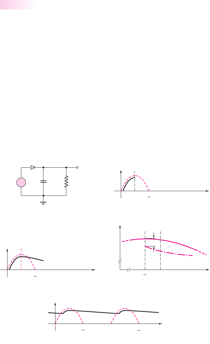
Filters, Ripple Voltage, and Diode Current
If a capacitor is added in parallel with the load resistor of a half-wave rectifier to form
a simple filter circuit (Figure 2.8(a)), we can begin to transform the half-wave sinu-
soidal output into a dc voltage. Figure 2.8(b) shows the positive half of the output
sine wave, and the beginning portion of the voltage across the capacitor, assuming
the capacitor is initially uncharged. If we assume that the diode forward resistance is
r
f
= 0
, which means that the
r
f
C
time constant is zero, the voltage across the ca-
pacitor follows this initial portion of the signal voltage. When the signal voltage
reaches its peak and begins to decrease, the voltage across the capacitor also starts to
decrease, which means the capacitor starts to discharge. The only discharge current
path is through the resistor. If the RC time constant is large, the voltage across the ca-
pacitor discharges exponentially with time (Figure 2.8(c)). During this time period,
the diode is cut off.
A more detailed analysis of the circuit response when the input voltage is near
its peak value indicates a subtle difference between actual circuit operation and the
qualitative description. If we assume that the diode turns off immediately when the
input voltage starts to decrease from its peak value, then the output voltage will de-
crease exponentially with time, as previously indicated. An exaggerated sketch of
these two voltages is shown in Figure 2.8(d). The output voltage decreases at a faster
rate than the input voltage, which means that at time
t
1
, the difference between
v
I
and
2.1.3
T
v
S
v
O
Time
T
2
3T
2
(e)
(b)
(c) (d)
v
S
v
O
Time
T
2
v
S
Time
T
2
v
O
ae
–t/RC
(a)
+
–
~
v
S
C
v
O
R
w tw t
1
v
v
S
a sin w t
v
O
ae
–t/RC
V
g
π
2
Figure 2.8 Simple filter circuit: (a) half-wave rectifier with an RC filter, (b) positive input
voltage and initial portion of output voltage, (c) output voltage resulting from capacitor
discharge, (d) expanded view of input and output voltages assuming capacitor discharge
begins at
ωt = π/2
, and (e) steady-state input and output voltages
nea80644_ch02_067-124.qxd 06/08/2009 07:28 PM Page 75 F506 Tempwork:Dont' Del Rakesh:June:Rakesh 06-08-09:MHDQ134-02 Folder:M
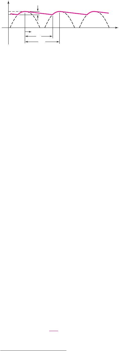
76 Part 1 Semiconductor Devices and Basic Applications
t
t'
T
p
V
r
V
M
V
L
v
O
T'
Figure 2.9 Output voltage of a full-wave rectifier with an RC filter showing the ripple voltage
v
O
, that is, the voltage across the diode, is greater than
V
γ
. However, this condition
cannot exist. Therefore, the diode does not turn off immediately. If the RC time
constant is large, there is only a small difference between the time of the peak input
voltage and the time the diode turns off. In this situation, a computer analysis may
provide more accurate results than an approximate hand analysis.
During the next positive cycle of the input voltage, there is a point at which the
input voltage is greater than the capacitor voltage, and the diode turns back on. The
diode remains on until the input reaches its peak value and the capacitor voltage is
completely recharged.
Since the capacitor filters out a large portion of the sinusoidal signal, it is called a fil-
ter capacitor. The steady-state output voltage of the RC filter is shown in Figure 2.8(e).
The ripple effect in the output from a full-wave filtered rectifier circuit can be seen
in the output waveform in Figure 2.9. The capacitor charges to its peak voltage value
when the input signal is at its peak value. As the input decreases, the diode becomes
reverse biased and the capacitor discharges through the output resistance R. Deter-
mining the ripple voltage is necessary for the design of a circuit with an acceptable
amount of ripple.
To a good approximation, the output voltage, that is, the voltage across the ca-
pacitor or the RC circuit, can be written as
v
O
(t) = V
M
e
−t
/τ
= V
M
e
−t
/RC
(2.3)
where
t
is the time after the output has reached its peak value, and RC is the time
constant of the circuit.
The smallest output voltage is
V
L
= V
M
e
−T
/RC
(2.4)
where
T
is the discharge time, as indicated in Figure 2.9.
The ripple voltage
V
r
is defined as the difference between
V
M
and
V
L
, and is
determined by
V
r
= V
M
− V
L
= V
M
(1 − e
−T
/RC
)
(2.5)
Normally, we will want the discharge time
T
to be small compared to the time
constant, or
T
RC
. Expanding the exponential in a series and keeping only the
linear terms of that expansion, we have the approximation
2
e
−T
/RC
∼
=
1 −
T
RC
(2.6)
2
We can show that the difference between the exponential function and the linear approximation given by
Equation (2.6) is less than 0.5 percent for
RC = 10T
. We need a relatively large RC time constant for this
application.
nea80644_ch02_067-124.qxd 06/08/2009 07:28 PM Page 76 F506 Tempwork:Dont' Del Rakesh:June:Rakesh 06-08-09:MHDQ134-02 Folder:M

Chapter 2 Diode Circuits 77
The ripple voltage can now be written as
V
r
∼
=
V
M
T
RC
(2.7)
Since the discharge time
T
depends on the RC time constant, Equation (2.7) is
difficult to solve. However, if the ripple effect is small, then as an approximation, we
can let
T
= T
p
, so that
V
r
∼
=
V
M
T
p
RC
(2.8)
where
T
p
is the time between peak values of the output voltage. For a full-wave
rectifier,
T
p
is one-half the signal period. Therefore, we can relate
T
p
to the signal
frequency,
f =
1
2T
p
The ripple voltage is then
V
r
=
V
M
2 fRC
(2.9)
For a half-wave rectifier, the time
T
p
corresponds to a full period (not a half pe-
riod) of the signal, so the factor 2 does not appear in Equation (2.9). The factor of 2
shows that the full-wave rectifier has half the ripple voltage of the half-wave rectifier.
Equation (2.9) can be used to determine the capacitor value required for a par-
ticular ripple voltage.
EXAMPLE 2.3
Objective: Determine the capacitance required to yield a particular ripple voltage.
Consider a full-wave rectifier circuit with a 60 Hz input signal and a peak output
voltage of
V
M
= 10
V. Assume the output load resistance is
R = 10 k
and the rip-
ple voltage is to be limited to
V
r
= 0.2
V.
Solution: From Equation (2.9), we can write
C =
V
M
2 fRV
r
=
10
2(60)(10 × 10
3
)(0.2)
⇒ 41.7 μF
Comment: If the ripple voltage is to be limited to a smaller value, a larger filter ca-
pacitor must be used. Note that the size of the ripple voltage and the size of filter
capacitor are related to the load resistance R.
EXERCISE PROBLEM
Ex 2.3: Assume the input signal to a rectifier circuit has a peak value of
V
M
= 12
V and is at a frequency of 60 Hz. Assume the output load resistance is
R = 2k
and the ripple voltage is to be limited to
V
r
= 0.4
V. Determine the
capacitance required to yield this specification for a (a) full-wave rectifier and
(b) half-wave rectifier. (Ans. (a)
C = 125 μ
F, (b)
C = 250 μ
F).
nea80644_ch02_067-124.qxd 06/08/2009 07:28 PM Page 77 F506 Tempwork:Dont' Del Rakesh:June:Rakesh 06-08-09:MHDQ134-02 Folder:M