Neamen D. Microelectronics: Circuit Analysis and Design
Подождите немного. Документ загружается.


58 Part 1 Semiconductor Devices and Basic Applications
1.4 (a) Find the concentration of electrons and holes in a sample of germanium
that has a concentration of donor atoms equal to
10
15
cm
−3
.
Is the semicon-
ductor n-type or p-type? (b) Repeat part (a) for silicon.
1.5 Gallium arsenide is doped with acceptor impurity atoms at a concentration
of
10
16
cm
−3
.
(a) Find the concentration of electrons and holes. Is the semi-
conductor n-type or p-type? (b) Repeat part (a) for germanium.
1.6 Silicon is doped with
5 × 10
16
arsenic atoms/cm
3
. (a) Is the material n- or
p-type? (b) Calculate the electron and hole concentrations at
T = 300 K
.
(c) Repeat part (b) for
T = 350 K
.
1.7 (a) Calculate the concentration of electrons and holes in silicon that has a
concentration of acceptor atoms equal to
5 × 10
16
cm
−3
.
Is the semicon-
ductor n-type or p-type? (b) Repeat part (a) for GaAs.
1.8 A silicon sample is fabricated such that the hole concentration is
p
o
= 2 ×10
17
cm
−3
.
(a) Should boron or arsenic atoms be added to the
intrinsic silicon? (b) What concentration of impurity atoms must be added?
(c) What is the concentration of electrons?
1.9 The electron concentration in silicon at
T = 300 K
is
n
o
= 5 ×10
15
cm
−3
.
(a) Determine the hole concentration. (b) Is the material n-type or p-type?
(c) What is the impurity doping concentration?
1.10 (a) A silicon semiconductor material is to be designed such that the major-
ity carrier electron concentration is
n
o
= 7 ×10
15
cm
−3
. Should donor or
acceptor impurity atoms be added to intrinsic silicon to achieve this electron
concentration? What concentration of dopant impurity atoms is required?
(b) In this silicon material, the minority carrier hole concentration is to
be no larger than
p
o
= 10
6
cm
−3
. Determine the maximum allowable
temperature.
1.11 (a) The applied electric field in p-type silicon is
E = 10 V/cm.
The semi-
conductor conductivity is
σ = 1.5 (–cm)
−1
and the cross-sectional area is
A = 10
−5
cm
2
.
Determine the drift current. (b) The cross-sectional area of
a semiconductor is
A = 2 ×10
−4
cm
2
and the resistivity is
ρ = 0.4
(–cm).
If the drift current is
I = 1.2mA,
what applied electric field must
be applied?
1.12 A drift current density of 120 A/cm
2
is established in n-type silicon with an
applied electric field of 18 V/cm. If the electron and hole mobilities are
μ
n
= 1250 cm
2
/V–s
and
μ
p
= 450 cm
2
/V–s,
respectively, determine the
required doping concentration.
1.13 An n-type silicon material has a resistivity of
ρ = 0.65 –cm.
(a) If the
electron mobility is
μ
n
= 1250 cm
2
/V–s,
what is the concentration of
donor atoms? (b) Determine the required electric field to establish a drift
current density of
J = 160 A/cm
2
.
1.14 (a) The required conductivity of a silicon material must be
σ = 1.5 (–cm)
−1
.
If
μ
n
= 1000 cm
2
/V–s
and
μ
p
= 375 cm
2
/V–s,
what
concentration of donor atoms must be added? (b) The required conductivity
of a silicon material must be
σ = 0.8 (–cm)
−1
.
If
μ
n
= 1200 cm
2
/V–s
and
μ
p
= 400 cm
2
/V–s,
what concentration of acceptor atoms must be
added?
1.15 In GaAs, the mobilities are
μ
n
= 8500 cm
2
/V–s
and
μ
p
= 400 cm
2
/
V–s.
(a) Determine the range in conductivity for a range in donor concentration
of
10
15
≤ N
d
≤ 10
19
cm
−3
. (b) Using the results of part (a), determine the
range in drift current density if the applied electric field is
E = 0.10 V/cm
.
nea80644_ch01_07-066.qxd 06/08/2009 05:16 PM Page 58 F506 Tempwork:Dont' Del Rakesh:June:Rakesh 06-08-09:MHDQ134-01 Folder:MHDQ134-01:

Chapter 1 Semiconductor Materials and Diodes 59
1.16 The electron and hole concentrations in a sample of silicon are shown in
Figure P1.16. Assume the electron and hole mobilities are the same as in
Problem 1.12. Determine the total diffusion current density versus distance
x for
0 ≤ x ≤ 0.001 cm.
1.17 The hole concentration in silicon is given by
p(x) = 10
4
+10
15
exp(−x/L
p
) x ≥ 0
The value of
L
p
is
10 μm
. The hole diffusion coefficient is
D
p
= 15 cm
2
/s
.
Determine the hole diffusion current density at (a)
x = 0
, (b)
x = 10 μm
,
and (c)
x = 30 μm
.
1.18 GaAs is doped to
N
a
= 10
17
cm
−3
. (a) Calculate
n
o
and
p
o
. (b) Excess elec-
trons and holes are generated such that
δn = δp = 10
15
cm
−3
. Determine
the total concentration of electrons and holes.
Section 1.2 The pn Junction
1.19 (a) Determine the built-in potential barrier
V
bi
in a silicon pn junction for (i)
N
d
= N
a
= 5 ×10
15
cm
−3
; (ii)
N
d
= 5 ×10
17
cm
−3
and
N
a
= 10
15
cm
−3
;
(iii)
N
a
= N
d
= 10
18
cm
−3
. (b) Repeat part (a) for GaAs.
1.20 Consider a silicon pn junction. The n-region is doped to a value of
N
d
= 10
16
cm
−3
. The built-in potential barrier is to be
V
bi
= 0.712 V.
Determine the required p-type doping concentration.
1.21 The donor concentration in the n-region of a silicon pn junction is
N
d
= 10
16
cm
−3
. Plot
V
bi
versus
N
a
over the range
10
15
≤ N
a
≤ 10
18
cm
−3
where
N
a
is the acceptor concentration in the p-region.
1.22 Consider a uniformly doped GaAs pn junction with doping concentrations
of
N
a
= 5 ×10
18
cm
−3
and
N
d
= 5 ×10
16
cm
−3
. Plot the built-in potential
barrier
V
bi
versus temperature for
200 K ≤ T ≤ 500 K
.
1.23 The zero-biased junction capacitance of a silicon pn junction is
C
jo
= 0.4pF
. The doping concentrations are
N
a
= 1.5 ×10
16
cm
−3
and
Carrier
concentration (cm
–3
)
Electron
concentration
Hole
concentration
x = 0 x = 0.001cm
10
16
10
12
10
16
10
12
Figure P1.16
nea80644_ch01_07-066.qxd 06/08/2009 05:16 PM Page 59 F506 Tempwork:Dont' Del Rakesh:June:Rakesh 06-08-09:MHDQ134-01 Folder:MHDQ134-01:

60 Part 1 Semiconductor Devices and Basic Applications
N
d
= 4 ×10
15
cm
−3
. Determine the junction capacitance at (a)
V
R
= 1V
,
(b)
V
R
= 3V
, and (c)
V
R
= 5V
.
*1.24 The zero-bias capacitance of a silicon pn junction diode is
C
jo
= 0.02 pF
and the built-in potential is
V
bi
= 0.80 V
. The diode is reverse biased
through a 47-k
resistor and a voltage source. (a) For
t < 0
, the applied
voltage is 5 V and, at
t = 0
, the applied voltage drops to zero volts. Estimate
the time it takes for the diode voltage to change from 5 V to 1.5 V. (As an
approximation, use the average diode capacitance between the two voltage
levels.) (b) Repeat part (a) for an input voltage change from 0 V to 5 V and
a diode voltage change from 0 V to 3.5 V. (Use the average diode capaci-
tance between these two voltage levels.)
1.25 The doping concentrations in a silicon pn junction are
N
d
= 5 ×10
15
cm
−3
and
N
a
= 10
17
cm
−3
.
The zero-bias junction capacitance is
C
jo
= 0.60 pF.
An inductance of 1.50 mH is connected in parallel with the pn junction. Cal-
culate the resonant frequency
f
o
of the circuit for reverse-bias voltages of
(a)
V
R
= 1V,
(b)
V
R
= 3V,
and (c)
V
R
= 5V.
1.26 (a) At what reverse-bias voltage does the reverse-bias current in a silicon pn
junction diode reach 90 percent of its saturation value? (b) What is the ratio
of the current for a forward-bias voltage of 0.2 V to the current for a reverse-
bias voltage of 0.2 V?
1.27 (a) The reverse-saturation current of a pn junction diode is
I
S
= 10
−11
A.
Determine the diode current for diode voltages of 0.3, 0.5, 0.7,
−0.02, −0.2,
and
−2V.
(b) Repeat part (a) for
I
S
= 10
−13
A.
1.28 (a) The reverse-saturation current of a pn junction diode is
I
S
= 10
−11
A.
Determine the diode voltage to produce currents of (i) 10
μA,
100
μA,
1 mA, and (ii)
−5 × 10
−12
A.
(b) Repeat part (a) for
I
S
= 10
−13
A
and part
(a) (ii) for
−10
−14
A.
1.29 A silicon pn junction diode has an emission coefficient of
n = 1
. The diode
current is
I
D
= 1mA
when
V
D
= 0.7V
. (a) What is the reverse-bias satu-
ration current? (b) Plot, on the same graph,
log
10
I
D
versus
V
D
over the
range
0.1 ≤ V
D
≤ 0.7
V when the emission coefficient is (i)
n = 1
and
(ii)
n = 2
.
1.30 Plot
log
10
I
D
versus
V
D
over the range
0.1 ≤ V
D
≤ 0.7V
for (a)
I
S
=
10
−12
and (b)
I
S
= 10
−14
A
.
1.31 (a) Consider a silicon pn junction diode operating in the forward-bias region.
Determine the increase in forward-bias voltage that will cause a factor of 10
increase in current. (b) Repeat part (a) for a factor of 100 increase in current.
1.32 A pn junction diode has
I
S
= 2
nA. (a) Determine the diode voltage if
(i)
I
D
= 2A
and (ii)
I
D
= 20 A.
(b) Determine the diode current if
(i)
V
D
= 0.4V
and (ii)
V
D
= 0.65 V.
1.33 The reverse-bias saturation current for a set of diodes varies between
5 × 10
−14
≤ I
S
≤ 5 ×10
−12
A
. The diodes are all to be biased at
I
D
= 2mA
. What is the range of forward-bias voltages that must be applied?
1.34 (a) A germanium pn junction has a diode current of
I
D
= 1.5mA
when bi-
ased at
V
D
= 0.30 V.
What is the reverse-bias saturation current? (b) Using
the results of part (a), determine the diode current when the diode is biased
at (i)
V
D
= 0.35 V
and (ii)
V
D
= 0.25 V.
1.35 (a) The reverse-saturation current of a gallium arsenide pn junction diode is
I
S
= 10
−22
A.
Determine the diode current for diode voltages of 0.8, 1.0,
1.2,
−0.02, −0.2,
and
−2V.
(b) Repeat part (a) for
I
S
= 5 ×10
−24
A.
nea80644_ch01_07-066.qxd 06/08/2009 05:16 PM Page 60 F506 Tempwork:Dont' Del Rakesh:June:Rakesh 06-08-09:MHDQ134-01 Folder:MHDQ134-01:
Chapter 1 Semiconductor Materials and Diodes 61
*1.36 The reverse-saturation current of a silicon pn junction diode at
T = 300 K
is
I
S
= 10
−12
A
. Determine the temperature range over which
I
S
varies
from
0.5 × 10
−12
A
to
50 × 10
−12
A
.
*1.37 A silicon pn junction diode has an applied forward-bias voltage of 0.6 V.
Determine the ratio of current at
100
◦
C to that at
−55
◦
C.
Section 1.3 DC Diode Analysis
1.38 A pn junction diode is in series with a
1M
resistor and a 2.8 V power
supply. The reverse-saturation current of the diode is
I
S
= 5 ×10
−11
A.
(a) Determine the diode current and voltage if the diode is forward biased.
(b) Repeat part (a) if the diode is reverse biased.
1.39 Consider the diode circuit shown in Figure P1.39. The diode reverse-
saturation current is
I
S
= 10
−12
A
. Determine the diode current
I
D
and
diode voltage
V
D
.
*1.40 The diode in the circuit shown in Figure P1.40 has a reverse-saturation cur-
rent of
I
S
= 5 ×10
−13
A
. Determine the diode voltage and current.
1.41 (a) For the circuit shown in Figure P1.41(a), determine
I
D1
,I
D2
,V
D1
,
and
V
D2
for (i)
I
S1
= I
S2
= 10
−13
A
and (ii)
I
S1
= 5 ×10
−14
A, I
S2
= 5 ×10
−13
A.
(b) Repeat part (a) for the circuit shown in Figure P1.41(b).
1.42 (a) The reverse-saturation current of each diode in the circuit shown in Fig-
ure P1.42 is
I
S
= 6 ×10
−14
A.
Determine the input voltage
V
I
required to
produce an output voltage of
V
O
= 0.635 V.
(b) Repeat part (a) if the
1k
resistor is changed to
R = 500 .
1.43 (a) Consider the circuit shown in Figure P1.40. The value of
R
1
is reduced
to
R
1
= 10 k
and the cut-in voltage of the diode is
V
γ
= 0.7V
. Determine
I
D
and
V
D
. (b) Repeat part (a) if
R
1
= 50 k
.
1.44 Consider the circuit shown in Figure P1.44. Determine the diode current
I
D
and diode voltage
V
D
for (a)
V
γ
= 0.6V
and (b)
V
γ
= 0.7V
.
1.45 The diode cut-in voltage is
V
γ
= 0.7V
for the circuits shown in Figure
P1.45. Plot
V
O
and
I
D
versus
I
I
over the range
0 ≤ I
I
≤ 2mA
for the cir-
cuit shown in (a) Figure P1.45(a), (b) Figure P1.45(b), and (c) Figure
P1.45(c).
Figure P1.39
Figure P1.41
+
–
I
D
V
D
+5 V
–5 V
20 kΩ
Figure P1.40
+
–
+
–
V
PS
=
1.2 V
I
D
V
D
R
1
= 50 kΩ
R
2
=
30 kΩ
(a)
+
D
1
D
1
V
D1
+
V
D1
I
D1
I
D1
I
i
=
1 mA
I
i
=
1 mA
I
D2
+
D
2
V
D2
+
V
D2
(b)
I
D2
D
2
–
–
–
–
Figure P1.42
+
–
V
I
V
O
1 kΩ
Figure P1.44
+–
I
D
V
D
+5 V
2 kΩ
2 kΩ
2 kΩ
3 kΩ
nea80644_ch01_07-066.qxd 06/08/2009 05:16 PM Page 61 F506 Tempwork:Dont' Del Rakesh:June:Rakesh 06-08-09:MHDQ134-01 Folder:MHDQ134-01:
62 Part 1 Semiconductor Devices and Basic Applications
–
–
+
+
D
1
D
1
D
2
V
O
I
D
I
D2
I
I
R
F
1 kΩ
–
+
V
B
= 1 V
V
O
I
D
I
I
R
1
=
1 kΩ
R
F
=
1 kΩ
–
+
V
O
I
D1
I
I
(a)
(b)
(c)
Figure P1.46
V
PS
+
–
I
1
I
2
I
D
R
2
R
1
Figure P1.47
I
V
O
+5 V
20 kΩ
I
V
O
+2 V
5 kΩ
I
V
O
+5 V
–5 V
20 kΩ
20 kΩ
–8 V
20 kΩ
I
V
O
+5 V
–5 V
20 kΩ
(a) (b) (c) (d)
Figure P1.49
+
–
+
+
–
–
5 V
I
V
V
D
R = 4.7 kΩ
*1.46 The cut-in voltage of the diode shown in the circuit in Figure P1.46 is
V
γ
= 0.7V
. The diode is to remain biased “on” for a power supply voltage
in the range
5 ≤ V
PS
≤ 10 V
. The minimum diode current is to be
I
D
(min) =
2 mA. The maximum power dissipated in the diode is to be no
more than 10 mW. Determine appropriate values of
R
1
and
R
2
.
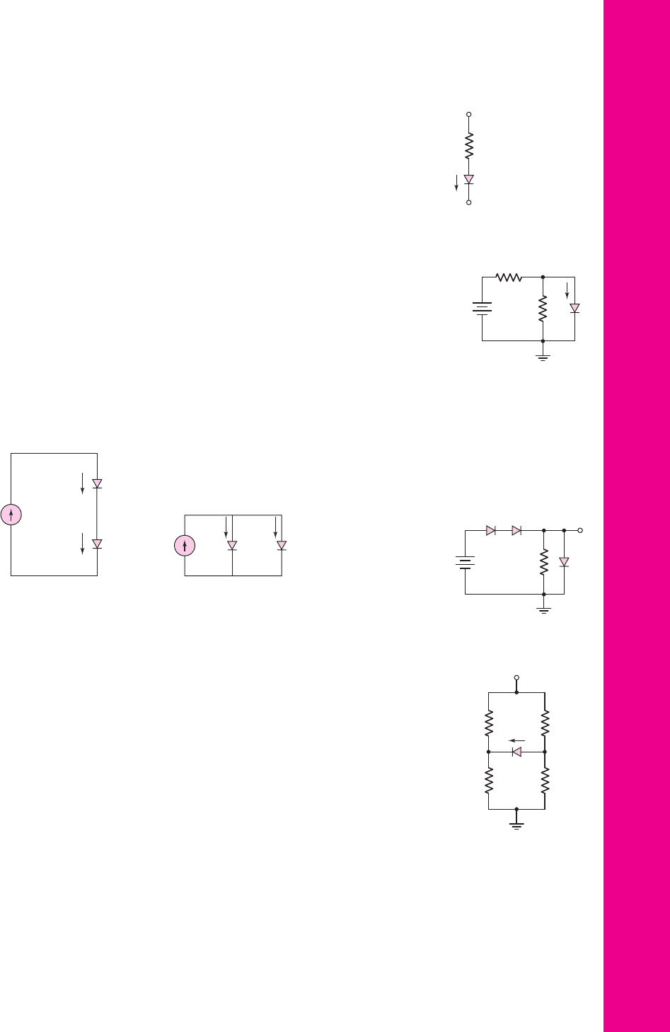
1.47 Find I and
V
O
in each circuit shown in Figure P1.47 if (i)
V
γ
= 0.7V
and
(ii)
V
γ
= 0.6V.
*1.48 Repeat Problem 1.47 if the reverse-saturation current for each diode is
I
S
= 5 ×10
−14
A.
What is the voltage across each diode?
1.49 (a) In the circuit shown in Figure P1.49, find the diode voltage
V
D
and the
supply voltage V such that the current is
I
D
= 0.4mA
. Assume the diode
cut-in voltage is
V
γ
= 0.7V
. (b) Using the results of part (a), determine the
power dissipated in the diode.
Figure P1.45
nea80644_ch01_07-066.qxd 06/08/2009 05:16 PM Page 62 F506 Tempwork:Dont' Del Rakesh:June:Rakesh 06-08-09:MHDQ134-01 Folder:MHDQ134-01:
1.50 Assume each diode in the circuit shown in Figure P1.50 has a cut-in voltage
of
V
γ
= 0.65 V
. (a) The input voltage is
V
I
= 5V
. Determine the value of
R
1
required such that
I
D1
is one-half the value of
I
D2
. What are the values
of
I
D1
and
I
D2
? (b) If
V
I
= 8V
and
R
1
= 2k
, determine
I
D1
and
I
D2
.
Chapter 1 Semiconductor Materials and Diodes 63
Figure P1.50
+
–
V
I
V
O
R
2
= 1 kΩ
I
D2
I
D1
R
1
Section 1.4 Small-Signal Diode Analysis
1.51 (a) Consider a pn junction diode biased at
I
DQ
= 1mA
. A sinusoidal volt-
age is superimposed on
V
DQ
such that the peak-to-peak sinusoidal current
is
0.05I
DQ
. Find the value of the applied peak-to-peak sinusoidal voltage.
(b) Repeat part (a) if
I
DQ
= 0.1mA
.
1.52 Determine the small-signal diffusion resistance
r
d
for a diode biased at
(a)
I
D
= 26 μA,
(b)
I
D
= 260 μA,
and (c)
I
D
= 2.6mA.
*1.53 The diode in the circuit shown in Figure P1.53 is biased with a constant cur-
rent source I. A sinusoidal signal
v
s
is coupled through
R
S
and C. Assume
that C is large so that it acts as a short circuit to the signal. (a) Show that the
sinusoidal component of the diode voltage is given by
v
o
= v
s
V
T
V
T
+ IR
S
(b) If
R
S
= 260
, find
v
o
/v
s
, for
I = 1
mA,
I = 0.1
mA, and
I =
0.01 mA.
Section 1.5 Other Types of Diodes
1.54 The forward-bias currents in a pn junction diode and a Schottky diode are
0.72 mA. The reverse-saturation currents are
I
S
= 5 ×10
−13
A
and
I
S
= 5 ×10
−8
A,
respectively. Determine the forward-bias voltage across
each diode.
1.55 A pn junction diode and a Schottky diode have equal cross-sectional areas
and have forward-bias currents of 0.5 mA. The reverse-saturation current of
the Schottky diode is
I
S
= 5 ×10
−7
A
. The difference in forward-bias volt-
ages between the two diodes is 0.30 V. Determine the reverse-saturation
current of the pn junction diode.
1.56 The reverse-saturation currents of a Schottky diode and a pn junction
diode are
I
S
= 5 ×10
−8
A
and
10
−12
A
, respectively. (a) The diodes are
connected in parallel and the parallel combination is driven by a constant
current of 0.5 mA. (i) Determine the current in each diode. (ii) Determine
the voltage across each diode. (b) Repeat part (a) for the diodes con-
nected in series, with a voltage of 0.90 V connected across the series
combination.
Figure P1.53
+
–
v
o
v
s
R
S
C
I
V
+
+
–
nea80644_ch01_07-066.qxd 06/08/2009 05:16 PM Page 63 F506 Tempwork:Dont' Del Rakesh:June:Rakesh 06-08-09:MHDQ134-01 Folder:MHDQ134-01:

*1.57 Consider the Zener diode circuit shown in Figure P1.57. The Zener break-
down voltage is
V
Z
= 5.6V
at
I
Z
= 0.1mA
, and the incremental Zener re-
sistance is
r
z
= 10
. (a) Determine
V
O
with no load (
R
L
=∞
). (b) Find
the change in the output voltage if
V
PS
changes by
±1V
. (c) Find
V
O
if
V
PS
= 10 V
and
R
L
= 2k
.
64 Part 1 Semiconductor Devices and Basic Applications
Figure P1.57
+
–
+
–
V
PS
= 10 V
I
Z
R
L
V
Z
V
O
R = 0.5 kΩ
1.58 (a) The Zener diode in Figure P1.57 is ideal with
V
Z
= 6.8V.
Determine
the maximum current and maximum power dissipated in the diode
(R
L
=∞).
(b) Determine the value of
R
L
such that
I
Z
is reduced to 0.1 of
its maximum value.
*1.59 Consider the Zener diode circuit shown in Figure P1.57. The Zener diode
voltage is
V
Z
= 6.8V
at
I
Z
= 0.1mA
and the incremental Zener resis-
tance is
r
z
= 20
. (a) Calculate
V
O
with no load (
R
L
=∞
). (b) Find the
change in the output voltage when a load resistance of
R
L
= 1k
is
connected.
1.60 The output current of a pn junction diode used as a solar cell can be given
by
I
D
= 0.2 −5 ×10
−14
exp
V
D
V
T
−1
A
The short-circuit current is defined as
I
SC
= I
D
when
V
D
= 0
and the open-
circuit voltage is defined as
V
OC
= V
D
when
I
D
= 0
. Find the values of
I
SC
and
V
OC
.
1.61 Using the current–voltage characteristics of the solar cell described in Prob-
lem 1.60, plot
I
D
versus
V
D
.
1.62 (a) Using the current–voltage characteristics of the solar cell described in
problem 1.60, determine
V
D
when
I
D
= 0.8I
SC
.
(b) Using the results of
part (a), determine the power supplied by the solar cell.
COMPUTER SIMULATION PROBLEMS
1.63 Use a computer simulation to generate the ideal current–voltage character-
istics of a diode from a reverse-bias voltage of 5 V to a forward-bias current
of 1 mA, for an
I
S
parameter value of (a)
10
−15
A
and (b)
10
−13
A.
Use the
default values for all other parameters.
1.64 Use a computer simulation to find the diode current and voltage for the
circuit described in Problem 1.38.
nea80644_ch01_07-066.qxd 06/10/2009 07:28 PM Page 64 F506 Tempwork:Dont' Del Rakesh:June:Rakesh 06-10-09:MHDQ134-01:

1.65 The reverse-saturation current for each diode in Figure P1.42 is
I
S
= 10
−14
A.
Use a computer simulation to plot the output voltage
V
O
ver-
sus the input voltage
V
I
over the range
0 ≤ V
I
≤ 2.0V.
1.66 Use a computer simulation to find the diode current, diode voltage, and out-
put voltage for each circuit shown in Figure P1.47. Assume
I
S
= 10
−13
A
for each diode.
DESIGN PROBLEMS
[Note: Each design should be verified by a computer simulation.]
*D1.67 Design a diode circuit to produce the load line and Q-point shown in Figure
P1.67. Assume diode piecewise linear parameters of
V
γ
= 0.7V
and
r
f
= 0.
Chapter 1 Semiconductor Materials and Diodes 65
*D1.68 Design a circuit to produce the characteristics shown in Figure P1.68, where
i
D
is the diode current and
v
I
is the input voltage. Assume diode piecewise
linear parameters of
V
γ
= 0.7V
and
r
f
= 0.
2.8
0.3
05
i
D
(mA)
I
(V)
–0.6
Figure P1.68
Figure P1.67
2.4
2.12
0.7 6 V0
i
D
(mA)
D
(V)
Q-point
nea80644_ch01_07-066.qxd 06/10/2009 07:29 PM Page 65 F506 Tempwork:Dont' Del Rakesh:June:Rakesh 06-10-09:MHDQ134-01:

*D1.70 Design a circuit to produce the characteristics shown in Figure P1.70, where
v
O
is the output voltage and
v
I
is the input voltage. Assume diode piecewise
linear parameters of
V
γ
= 0.7V
and
r
f
= 0.
66 Part 1 Semiconductor Devices and Basic Applications
2.13
0.7
0.7 5
O
(V)
I
(V)
Figure P1.69
Figure P1.70
O
(V)
I
(V)
– 4.0
–4.0
*D1.69 Design a circuit to produce the characteristics shown in Figure P1.69, where
v
O
is the output voltage and
v
I
is the input voltage. Assume diode piecewise
linear parameters of
V
γ
= 0.7V
and
r
f
= 0.
nea80644_ch01_07-066.qxd 06/08/2009 05:16 PM Page 66 F506 Tempwork:Dont' Del Rakesh:June:Rakesh 06-08-09:MHDQ134-01 Folder:MHDQ134-01:

Chapter
Diode Circuits
2
2
In the last chapter, we discussed some of the properties of semiconductor materials
and introduced the diode. We presented the ideal current–voltage relationship of the
diode and considered the piecewise linear model, which simplifies the dc analysis of
diode circuits. In this chapter, the techniques and concepts developed in Chapter 1
are used to analyze and design electronic circuits containing diodes. A general goal
of this chapter is to develop the ability to use the piecewise linear model and approx-
imation techniques in the hand analysis and design of various diode circuits.
Each circuit to be considered accepts an input signal at a set of input terminals
and produces an output signal at a set of output terminals. This process is called
signal processing. The circuit “processes” the input signal and produces an output
signal that is a different shape or a different function compared to the input signal.
We will see in this chapter how diodes are used to perform these various signal
processing functions.
Although diodes are useful electronic devices, we will begin to see the limita-
tions of these devices and the desirability of having some type of “amplifying”
device.
PREVIEW
In this chapter, we will:
• Determine the operation and characteristics of diode rectifier circuits, which,
in general, form the first stage of the process of converting an ac signal into a
dc signal in the electronic power supply.
• Apply the characteristics of the Zener diode to a Zener diode voltage regula-
tor circuit.
• Apply the nonlinear characteristics of diodes to create waveshaping circuits
known as clippers and clampers.
• Examine the techniques used to analyze circuits that contain more than one
diode.
• Understand the operation and characteristics of specialized photodiode and
light-emitting diode circuits.
• Design a basic dc power supply incorporating a filtered rectifier circuit and a
Zener diode.
67
nea80644_ch02_067-124.qxd 06/08/2009 07:28 PM Page 67 F506 Tempwork:Dont' Del Rakesh:June:Rakesh 06-08-09:MHDQ134-02 Folder:M