Neamen D. Microelectronics: Circuit Analysis and Design
Подождите немного. Документ загружается.

78 Part 1 Semiconductor Devices and Basic Applications
t
V
r
v
O
Δt
t
i
D
v
i
D, max
T
(a)
(b)
T
2
t = 0
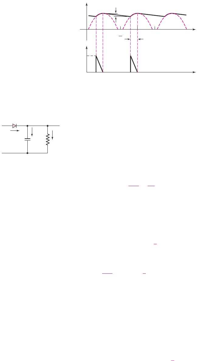
Figure 2.10 Output of a full-wave rectifier with an RC filter: (a) diode conduction time and
(b) diode current
The diode in a filtered rectifier circuit conducts for a brief interval
t
near the
peak of the sinusoidal input signal. The diode current supplies the charge lost by the
capacitor during the discharge time. Figure 2.10 shows the rectified output of a full-
wave rectifier and the filtered output assuming ideal diodes
(V
γ
= 0)
in the rectifier
circuit. We will use this approximate model to estimate the diode current during the
diode conduction time. Figure 2.11 shows the equivalent circuit of the full-wave rec-
tifier during the charging time. We see that
i
D
= i
C
+i
R
= C
dv
O
dt
+
v
O
R
(2.10)
During the diode conduction time near
t = 0
(Figure 2.10), we can write
v
O
= V
M
cos ωt
(2.11)
For small ripple voltages, the diode conduction time is small, so we can approximate
the output voltage as
v
O
= V
M
cos ωt
∼
=
V
M
1 −
1
2
(ωt)
2
(2.12)
The charging current through the capacitor is
i
C
= C
dv
O
dt
= CV
M
−
1
2
(2)(ωt)(ω)
=−ωCV
M
ωt
(2.13)
From Figure 2.10, the diode conduction occurs during the time
−t < t < 0
, so that
the capacitor current is positive and is a linear function of time. We note that at
t = 0
,
the capacitor current is
i
C
= 0
. At
t =−t
, the capacitor charging current is at a
peak value and is given by
i
C,peak
=−ωCV
M
[
ω(−t)
]
=+ωCV
M
ωt
(2.14)
The capacitor current during the diode charging time is approximately triangular
and is shown in Figure 2.10(b).
From Equation (2.11), we can write that the voltage
V
L
is given by
V
L
= V
M
cos[ω(−t)]
∼
=
V
M
1 −
1
2
(ωt)
2
(2.15)
+
–
v
S
i
D
RC
i
R
i
C
v
O
Figure 2.11 Equivalent
circuit of a full-wave rectifier
during capacitor charging
cycle
nea80644_ch02_067-124.qxd 06/08/2009 07:28 PM Page 78 F506 Tempwork:Dont' Del Rakesh:June:Rakesh 06-08-09:MHDQ134-02 Folder:M

Chapter 2 Diode Circuits 79
Solving for
ωt
, we find
ωt =
2V
r
V
M
(2.16)
where
V
r
= V
M
− V
L
.
From Equation (2.9), we can write
fC =
V
M
2RV
r
(2.17(a))
or
2π fC = ωC =
π V
M
RV
r
(2.17(b))
Substituting Equations (2.17(b)) and (2.16) into Equation (2.14), we have
i
C,peak
=
π V
M
RV
r
V
M
2V
r
V
M
(2.18(a))
or
i
C,peak
= π
V
M
R
2V
M
V
r
(2.18(b))
Since the charging current through the capacitor is triangular, we have that the aver-
age capacitor current during the diode charging time is
i
C,avg
=
π
2
V
M
R
2V
M
V
r
(2.19)
During the capacitor charging time, there is still a current through the load. This cur-
rent is also being supplied through the diode. Neglecting the ripple voltage, the load
current is approximately
i
L
∼
=
V
M
R
(2.20)
Therefore, the peak diode current during the diode conduction time for a full-wave
rectifier is approximately
i
D,peak
∼
=
V
M
R
1 + π
2V
M
V
r
(2.21)
and the average diode current during the diode conduction time is
i
D,avg
∼
=
V
M
R
1 +
π
2
2V
M
V
r
(2.22)
The average diode current over the entire input signal period is
i
D
(avg) =
V
M
R
1 +
π
2
2V
M
V
t
T
(2.23)
For the full-wave rectifier, we have
1/2T = f
,so
t =
1
ω
2V
r
V
M
=
1
2π f
2V
r
V
M
(2.24(a))
nea80644_ch02_067-124.qxd 06/08/2009 07:28 PM Page 79 F506 Tempwork:Dont' Del Rakesh:June:Rakesh 06-08-09:MHDQ134-02 Folder:M

80 Part 1 Semiconductor Devices and Basic Applications
Then
t
T
=
1
2π f
2V
r
V
M
2 f =
1
π
2V
r
V
M
(2.24(b))
Then the average current through the diode during the entire cycle for a full-wave
rectifier is
i
D
(avg) =
1
π
2V
r
V
M
V
M
R
1 +
π
2
2V
M
V
r
(2.25)
DESIGN EXAMPLE 2.4
Objective: Design a full-wave rectifier to meet particular specifications.
A full-wave rectifier is to be designed to produce a peak output voltage of 12 V,
deliver 120 mA to the load, and produce an output with a ripple of not more than
5 percent. An input line voltage of 120 V (rms), 60 Hz is available.
Solution: A full-wave bridge rectifier will be used, because of the advantages previ-
ously discussed. The effective load resistance is
R =
V
O
I
L
=
12
0.12
= 100
Assuming a diode cut-in voltage of 0.7 V, the peak value of
v
S
is
v
S
(max) = v
O
(max) + 2V
γ
= 12 +2(0.7) = 13.4V
For a sinusoidal signal, this produces an rms voltage value of
v
S,rms
=
13.4
√
2
= 9.48 V
The transformer turns ratio is then
N
1
N
2
=
120
9.48
= 12.7
For a 5 percent ripple, the ripple voltage is
V
r
= (0.05)V
M
= (0.05)(12) = 0.6V
The required filter capacitor is found to be
C =
V
M
2 fRV
r
=
12
2(60)(100)(0.6)
⇒ 1667 μF
The peak diode current, from Equation (2.21), is
i
D,peak
=
12
100
1 + π
2(12)
0.6
= 2.50 A
and the average diode current over the entire signal period, from Equation (2.25), is
i
D
(avg) =
1
π
2(0.6)
12
12
100
1 +
π
2
2(12)
0.6
⇒ 132 mA
Finally, the peak inverse voltage that each diode must sustain is
PIV = v
R
(max) = v
S
(max) − V
γ
= 13.4 −0.7 = 12.7V
nea80644_ch02_067-124.qxd 06/08/2009 07:28 PM Page 80 F506 Tempwork:Dont' Del Rakesh:June:Rakesh 06-08-09:MHDQ134-02 Folder:M
Chapter 2 Diode Circuits 81
Comment:
The minimum specifications for the diodes in this full-wave rectifier cir-
cuit are: a peak current of 2.50 A, an average current of 132 mA, and a peak inverse
voltage of 12.7 V. In order to meet the desired ripple specification, the required filter
capacitance must be large, since the effective load resistance is small.
Design Pointer: (1) A particular turns ratio was determined for the transformer.
However, this particular transformer design is probably not commercially available.
This means an expensive custom transformer design would be required, or if a stan-
dard transformer is used, then additional circuit design is required to meet the
output voltage specification. (2) A constant 120 V (rms) input voltage is assumed to
be available. However, this voltage can fluctuate, so the output voltage will also
fluctuate.
We will see later how more sophisticated designs will solve these two problems.
Computer Verification: Since we simply used an assumed cut-in voltage for the
diode and used approximations in the development of the ripple voltage equations,
we can use PSpice to give us a more accurate evaluation of the circuit. The PSpice
circuit schematic and the steady-state output voltage are shown in Figure 2.12. We
see that the peak output voltage is 11.6 V, which is close to the desired 12 V. One
reason for the slight discrepancy is that the diode voltage drop for the maximum
input voltage is slightly greater than 0.8 V rather than the assumed 0.7 V. The ripple
voltage is approximately 0.5 V, which is within the 0.6 V specification.
Discussion: In the PSpice simulation, a standard diode, 1N4002, was used. In order
for the computer simulation to be valid, the diode used in the simulation and in the
actual circuit must match. In this example, to reduce the diode voltage and increase
the peak output voltage, a diode with a larger cross-sectional area should be used.
v
3
D
3
1N4002
D
2
1N4002
D
4
1N4002
V
out
V
out
(V)
D
1
1N4002
C
1
1667 mF
R
1
100 Ω
(a)
(b)
12
0
11
0204060
Time (ms)
+
–
~
Figure 2.12 (a) PSpice circuit schematic of diode bridge circuit with an RC filter;
(b) Steady-state output voltage of PSpice analysis of diode bridge circuit for a 60 Hz input
sine wave with a peak value of 13.4 V
nea80644_ch02_067-124.qxd 06/08/2009 07:28 PM Page 81 F506 Tempwork:Dont' Del Rakesh:June:Rakesh 06-08-09:MHDQ134-02 Folder:M

82 Part 1 Semiconductor Devices and Basic Applications
EXERCISE PROBLEM
Ex 2.4: The input voltage to the half-wave rectifier in Figure 2.8(a) is
v
S
= 75 sin[2π(60)t]
V. Assume a diode cut-in voltage of
V
γ
= 0
. The ripple
voltage is to be no more than
V
r
= 4
V. If the filter capacitor is 50
μ
F, determine
the minimum load resistance that can be connected to the output. (Ans.
R =
6.25 k
)
Detectors
One of the first applications of semiconductor diodes was as a detector for amplitude-
modulated (AM) radio signals. An amplitude-modulated signal consists of a radio-
frequency carrier wave whose amplitude varies with an audio frequency as shown in
Figure 2.13(a). The detector circuit is shown in Figure 2.13(b) and is a half-wave rec-
2.1.4
t
v
in
v
OUT
t
v
in
v
OUT
+
–
RC
(a)
(b)
(c)
Figure 2.13 The signals and circuit for demodulation of an amplitude-modulated signal.
(a) The amplitude-modulated input signal. (b) The detector circuit. (c) The demodulated
output signal.
nea80644_ch02_067-124.qxd 06/08/2009 07:28 PM Page 82 F506 Tempwork:Dont' Del Rakesh:June:Rakesh 06-08-09:MHDQ134-02 Folder:M
Chapter 2 Diode Circuits 83
tifier circuit with an RC filter on the output. For this application, the RC time constant
should be approximately equal to the period of the carrier signal, so that the output
voltage can follow each peak value of the carrier signal. If the time constant is too
large, the output will not be able to change fast enough and the output will not repre-
sent the audio output. The output of the detector is shown in Figure 2.13(c).
The output of the detector circuit is then coupled to an amplifier through a
capacitor to remove the dc component of the signal, and the output of the amplifier is
then fed to a speaker.
Voltage Doubler Circuit
A voltage doubler circuit is very similar to the full-wave rectifier, except that two
diodes are replaced by capacitors, and it can produce a voltage equal to approxi-
mately twice the peak output of a transformer (Figure 2.14).
Figure 2.15(a) shows the equivalent circuit when the voltage polarity at the “top”
of the transformer is negative; Figure 2.15(b) shows the equivalent circuit for the op-
posite polarity. In the circuit in Figure 2.15(a), the forward diode resistance of D
2
is
small; therefore, the capacitor C
1
will charge to almost the peak value of
v
S
. Termi-
nal 2 on C
1
is positive with respect to terminal 1. As the magnitude of
v
S
decreases
from its peak value, C
1
discharges through R
L
and C
2
. We assume that the time con-
stant R
L
C
2
is very long compared to the period of the input signal.
As the polarity of
v
S
changes to that shown in Figure 2.15(b), the voltage across C
1
is essentially constant at V
M
, with terminal 2 remaining positive. As
v
S
reaches its max-
imum value, the voltage across C
2
essentially becomes V
M
. By Kirchhoff’s voltage law,
2.1.5
+
––
v
I
+
v
S
+–
v
O
R
L
D
1
D
2
C
2
C
1
Figure 2.14 A voltage doubler circuit
(a) (b)
+
–
v
S
+
–
v
O
C
1
C
2
D
1
R
L
1
2
2 1
+
–
v
S
+
–
v
O
C
2
C
1
D
2
R
L
1
2
2 1
Figure 2.15 Equivalent circuit of the voltage doubler circuit: (a) negative input cycle and (b)
positive input cycle
nea80644_ch02_067-124.qxd 06/08/2009 07:28 PM Page 83 F506 Tempwork:Dont' Del Rakesh:June:Rakesh 06-08-09:MHDQ134-02 Folder:M

84 Part 1 Semiconductor Devices and Basic Applications
the peak voltage across R
L
is now essentially equal to 2V
M
, or twice the peak output of
the transformer. The same ripple effect occurs as in the output voltage of the rectifier
circuits, but if C
1
and C
2
are relatively large, then the ripple voltage V
r
, is quite small.
There are also voltage tripler and voltage quadrupler circuits. These circuits pro-
vide a means by which multiple dc voltages can be generated from a single ac source
and power transformer.
Test Your Understanding
TYU 2.1 Consider the circuit in Figure 2.4. The input voltage is
v
s
(t) =
15 sin ω t
(V) and the diode cut-in voltage is
V
γ
= 0.7
V. The voltage
V
B
varies
between
4 ≤ V
B
≤ 8
V. The peak current is to be limited to
i
D
(peak)
= 18
mA.
(a) Determine the minimum value of
R
. (b) Using the results of part (a), determine
the range in peak current and the range in duty cycle. (Ans. (a)
R = 572
;
(b)
11 ≤ i
D
(peak)
≤ 18
mA,
30.3 ≤
duty cycle
≤ 39.9%)
.
TYU 2.2 The circuit in Figure 2.5(a) is used to rectify a sinusoidal input signal with
a peak voltage of 120 V and a frequency of 60 Hz. A filter capacitor is connected in
parallel with R. If the output voltage cannot drop below 100 V, determine the required
value of the capacitance C. The transformer has a turns ratio of N
1
:
N
2
= 1
: 1, where
N
2
is the number of turns on each of the secondary windings. Assume the diode cut-
in voltage is 0.7 V and the output resistance is 2.5 k
. (Ans. C = 20.6
μ
F)
TYU 2.3 The secondary transformer voltage of the rectifier circuit shown in Fig-
ure 2.6(a) is
v
S
= 50 sin[2π(60)t]V
. Each diode has a cut-in voltage of
V
γ
= 0.7V
,
and the load resistance is R = 10 k
. Determine the value of the filter capacitor that
must be connected in parallel with R such that the ripple voltage is no greater than
V
r
= 2V
. (Ans.
C = 20.3 μ
F)
TYU 2.4 Determine the fraction (percent) of the cycle that each diode is conduct-
ing in (a) Exercise EX2.4, (b) Exercise TYU2.2, and (c) Exercise TYU2.3. (Ans.
(a) 5.2%, (b) 18.1%, (c) 9.14%)
2.2 ZENER DIODE CIRCUITS
Objective: • Apply the characteristics of the Zener diode to a Zener
diode voltage regulator circuit.
In Chapter 1, we saw that the breakdown voltage of a Zener diode was nearly con-
stant over a wide range of reverse-bias currents (Figure 1.21). This makes the Zener
diode useful in a voltage regulator, or a constant-voltage reference circuit. In this
chapter, we will look at an ideal voltage reference circuit, and the effects of includ-
ing a nonideal Zener resistance.
The Zener diode voltage regulator circuits designed in this section will then be
added to the design of the electronic power supply in Figure 2.1. We should note that
in actual power supply designs, the voltage regulator will be a more sophisticated
integrated circuit rather than the simpler Zener diode design that will be developed
nea80644_ch02_067-124.qxd 06/08/2009 07:28 PM Page 84 F506 Tempwork:Dont' Del Rakesh:June:Rakesh 06-08-09:MHDQ134-02 Folder:M

Chapter 2 Diode Circuits 85
here. One reason is that a standard Zener diode with a particular desired breakdown
voltage may not be available. However, this section will provide the basic concept of
a voltage regulator.
Ideal Voltage Reference Circuit
Figure 2.16 shows a Zener voltage regulator circuit. For this circuit, the output volt-
age should remain constant, even when the output load resistance varies over a fairly
wide range, and when the input voltage varies over a specific range. The variation in
V
PS
may be the ripple voltage from a rectifier circuit.
We determine, initially, the proper input resistance R
i
. The resistance R
i
limits
the current through the Zener diode and drops the “excess” voltage between
V
PS
and
V
Z
. We can write
2.2.1
+
–
V
PS
+
–
V
Z
R
i
+
–
V
L
I
Z
I
L
R
L
I
I
Figure 2.16 A Zener diode voltage regulator circuit
R
i
=
V
PS
− V
Z
I
I
=
V
PS
− V
Z
I
Z
+ I
L
(2.26)
which assumes that the Zener resistance is zero for the ideal diode. Solving this equa-
tion for the diode current, I
Z
, we get
I
Z
=
V
PS
− V
Z
R
i
− I
L
(2.27)
where
I
L
= V
Z
/R
L
, and the variables are the input voltage source V
PS
and the load
current I
L
.
For proper operation of this circuit, the diode must remain in the breakdown re-
gion and the power dissipation in the diode must not exceed its rated value. In other
words:
1. The current in the diode is a minimum, I
Z
(min), when the load current is a
maximum, I
L
(max), and the source voltage is a minimum, V
PS
(min).
2. The current in the diode is a maximum, I
Z
(max), when the load current is a
minimum, I
L
(min), and the source voltage is a maximum, V
PS
(max).
Inserting these two specifications into Equation (2.26), we obtain
R
i
=
V
PS
(min) − V
Z
I
Z
(min) + I
L
(max)
(2.28(a))
and
R
i
=
V
PS
(max) − V
Z
I
Z
(max) + I
L
(min)
(2.28(b))
nea80644_ch02_067-124.qxd 06/08/2009 07:28 PM Page 85 F506 Tempwork:Dont' Del Rakesh:June:Rakesh 06-08-09:MHDQ134-02 Folder:M

86 Part 1 Semiconductor Devices and Basic Applications
Equating these two expressions, we then obtain
[V
PS
(min) − V
Z
] · [I
Z
(max) + I
L
(min)]
= [V
PS
(max) − V
Z
] · [I
Z
(min) + I
L
(max)]
(2.29)
Reasonably, we can assume that we know the range of input voltage, the range
of output load current, and the Zener voltage. Equation (2.29) then contains two un-
knowns,
I
Z
(min)
and
I
Z
(max)
. Further, as a minimum requirement, we can set the
minimum Zener current to be one-tenth the maximum Zener current, or
I
Z
(min) =
0.1I
Z
(max)
. (More stringent design requirements may require the minimum Zener
current to be 20 to 30 percent of the maximum value.) We can then solve for
I
Z
(max)
, using Equation (2.29), as follows:
I
Z
(max) =
I
L
(max) · [V
PS
(max) − V
Z
] − I
L
(min) · [V
PS
(min) − V
Z
]
V
PS
(min) − 0.9V
Z
−0.1V
PS
(max)
(2.30)
Using the maximum current thus obtained from Equation (2.30), we can determine
the maximum required power rating of the Zener diode. Then, combining Equa-
tion (2.30) with either Equation (2.28(a)) or (2.28(b)), we can determine the required
value of the input resistance R
i
.
DESIGN EXAMPLE 2.5
Objective: Design a voltage regulator using the circuit in Figure 2.16.
The voltage regulator is to power a car radio at
V
L
= 9
V from an automobile
battery whose voltage may vary between 11 and 13.6 V. The current in the radio will
vary between 0 (off) to 100 mA (full volume).
The equivalent circuit is shown in Figure 2.17.
Solution: The maximum Zener diode current can be determined from Equa-
tion (2.30) as
I
Z
(max) =
(100)[13.6 − 9] −0
11 − (0.9)(9) − (0.1)(13.6)
∼
=
300 mA
The maximum power dissipated in the Zener diode is then
P
Z
(max) = I
Z
(max) · V
Z
= (300)(9) ⇒ 2.7W
The value of the current-limiting resistor R
i
, from Equation (2.28(b)), is
R
i
=
13.6 − 9
0.3 + 0
= 15.3
R
i
I
I
I
Z
V
PS
=
11–13.6 V
V
Z
= 9 V
Radio
+
–
+
–
I
L
Figure 2.17 Circuit for Design Example 2.5
nea80644_ch02_067-124.qxd 06/08/2009 07:28 PM Page 86 F506 Tempwork:Dont' Del Rakesh:June:Rakesh 06-08-09:MHDQ134-02 Folder:M

Chapter 2 Diode Circuits 87
The maximum power dissipated in this resistor is
P
Ri
(max) =
(V
PS
(max) − V
Z
)
2
R
i
=
(13.6 − 9)
2
15.3
∼
=
1.4W
We find
I
Z
(min) =
11 − 9
15.3
−0.10 ⇒ 30.7mA
Comment: From this design, we see that the minimum power ratings of the
Zener diode and input resistor are 2.7 W and 1.4 W, respectively. The minimum
Zener diode current occurs for V
PS
(min) and I
L
(max). We find I
Z
(min) = 30.7
mA, which is approximately 10 percent of I
Z
(max) as specified by the design
equations.
Design Pointer: (1) The variable input in this example was due to a variable battery
voltage. However, referring back to Example 2.4, the variable input could also be a
function of using a standard transformer with a given turns ratio as opposed to a cus-
tom design with a particular turns ratio and/or having a 120 V (rms) input voltage that
is not exactly constant.
(2) The 9 V output is a result of using a 9 V Zener diode. However, a Zener diode
with exactly a 9 V breakdown voltage may also not be available. We will again see
later how more sophisticated designs can solve this problem.
EXERCISE PROBLEM
Ex 2.5: The Zener diode regulator circuit shown in Figure 2.16 has an input volt-
age that varies between 10 and 14 V, and a load resistance that varies between
R
L
= 20
and 100 . Assume a 5.6 Zener diode is used, and assume
I
Z
(min) =
0.1I
Z
(max)
. Find the value of R
i
required and the minimum power rating of the
diode. (Ans.
P
Z
= 3.31
W,
R
i
∼
=
13
)
The operation of the Zener diode circuit shown in Figure 2.17 can be visualized
by using load lines. Summing currents at the Zener diode, we have
v
PS
− V
Z
R
i
= I
Z
+
V
Z
R
L
(2.31)
Solving for V
Z
, we obtain
V
Z
= v
PS
R
L
R
i
+ R
L
− I
Z
R
i
R
L
R
i
+ R
L
(2.32)
which is the load line equation. Using the parameters of Example 2.5, the load resis-
tance varies from
R
L
=∞(I
L
= 0)
to
R
L
= 9/0.1 = 90 (I
L
= 100 mA
). The
current limiting resistor is
R
i
= 15
and the input voltage varies over the range
11 ≤ v
PS
≤ 13.6V
.
We may write load line equations for the various circuit conditions.
A:
v
PS
= 11 V
,
R
L
=∞
;
V
Z
= 11 − I
Z
(15)
B:
v
PS
= 11 V
,
R
L
= 90
;
V
Z
= 9.43 − I
Z
(12.9)
C:
v
PS
= 13.6V
,
R
L
=∞
;
V
Z
= 13.6 − I
Z
(15)
D:
v
PS
= 13.6V
,
R
L
= 90
;
V
Z
= 11.7 − I
Z
(12.9)
nea80644_ch02_067-124.qxd 06/08/2009 07:28 PM Page 87 F506 Tempwork:Dont' Del Rakesh:June:Rakesh 06-08-09:MHDQ134-02 Folder:M