Neamen D. Microelectronics: Circuit Analysis and Design
Подождите немного. Документ загружается.


48 Part 1 Semiconductor Devices and Basic Applications
Test Your Understanding
TYU 1.12 Determine the diffusion conductance of a pn junction diode at
T = 300
K
and biased at a current of 0.8 mA. (Ans.
g
d
= 30.8
mS)
TYU 1.13 Determine the small-signal diffusion resistance of a pn junction diode at
I
D
= 10 μA, 100 μA,
and 1 mA. (Ans.
2.6k, 260 ,26 ).
TYU 1.14 The diffusion resistance of a pn junction diode at
T = 300
K is deter-
mined to be
r
d
= 50
. What is the quiescent diode current? (Ans.
I
DQ
= 0.52
mA)
1.5 OTHER DIODE TYPES
Objective: • Gain an understanding of the properties and character-
istics of a few specialized diodes.
There are many other types of diodes with specialized characteristics that are
useful in particular applications. We will briefly consider only a few of these diodes.
We will consider the solar cell, photodiode, light-emitting diode, Schottky diode, and
Zener diode.
Solar Cell
A solar cell is a pn junction device with no voltage directly applied across the junc-
tion. The pn junction, which converts solar energy into electrical energy, is connected
to a load as indicated in Figure 1.39. When light hits the space-charge region, elec-
trons and holes are generated. They are quickly separated and swept out of the space-
charge region by the electric field, thus creating a photocurrent. The generated
photocurrent will produce a voltage across the load, which means that the solar cell
has supplied power. Solar cells are usually fabricated from silicon, but may be made
from GaAs or other III–V compound semiconductors.
Solar cells have long been used to power the electronics in satellites and space
vehicles, and also as the power supply to some calculators. Solar cells are also used
to power race cars in a Sunrayce event. Collegiate teams in the United States design,
1.5.1
E-field
Solar energy
R
L
I
ph
V
p n
Photocurrent
– +
Figure 1.39 A pn junction solar cell connected to load
nea80644_ch01_07-066.qxd 06/08/2009 05:15 PM Page 48 F506 Tempwork:Dont' Del Rakesh:June:Rakesh 06-08-09:MHDQ134-01 Folder:MHDQ134-01:

Chapter 1 Semiconductor Materials and Diodes 49
build and drive the race cars. Typically, a Sunrayce car has 8 m
2
of solar cell arrays
that can produce 800 W of power on a sunny day at noon. The power from the solar
array can be used either to power an electric motor or to charge a battery pack.
Photodiode
Photodetectors are devices that convert optical signals into electrical signals. An
example is the photodiode, which is similar to a solar cell except that the pn junction
is operated with a reverse-bias voltage. Incident photons or light waves create excess
electrons and holes in the space-charge region. These excess carriers are quickly sep-
arated and swept out of the space-charge region by the electric field, thus creating a
“photocurrent.” This generated photocurrent is directly proportional to the incident
photon flux.
Light-Emitting Diode
The light-emitting diode (LED) converts current to light. As previously explained,
when a forward-bias voltage is applied across a pn junction, electrons and holes flow
across the space-charge region and become excess minority carriers. These excess
minority carriers diffuse into the neutral semiconductor regions, where they recom-
bine with majority carriers. If the semiconductor is a direct bandgap material, such
as GaAs, the electron and hole can recombine with no change in momentum, and a
photon or light wave can be emitted. Conversely, in an indirect bandgap material,
such as silicon, when an electron and hole recombine, both energy and momentum
must be conserved, so the emission of a photon is very unlikely. Therefore, LEDs
are fabricated from GaAs or other compound semiconductor materials. In an LED,
the diode current is directly proportional to the recombination rate, which means
that the output light intensity is also proportional to the diode current.
Monolithic arrays of LEDs are fabricated for numeric and alphanumeric dis-
plays, such as the readout of a digital voltmeter.
An LED may be integrated into an optical cavity to produce a coherent photon
output with a very narrow bandwidth. Such a device is a laser diode, which is used in
optical communications applications.
The LED can be used in conjunction with a photodiode to create an optical sys-
tem such as that shown in Figure 1.40. The light signal created may travel over
1.5.3
1.5.2
Input
signal
Output
signal
Transmitter
Drive
circuit
Receiver
LED
Photodiode
Amplifier
Optical
fiber
Figure 1.40 Basic elements in an optical transmission system
nea80644_ch01_07-066.qxd 06/08/2009 05:15 PM Page 49 F506 Tempwork:Dont' Del Rakesh:June:Rakesh 06-08-09:MHDQ134-01 Folder:MHDQ134-01:
50 Part 1 Semiconductor Devices and Basic Applications
relatively long distances through the optical fiber, because of the low optical absorp-
tion in high-quality optical fibers.
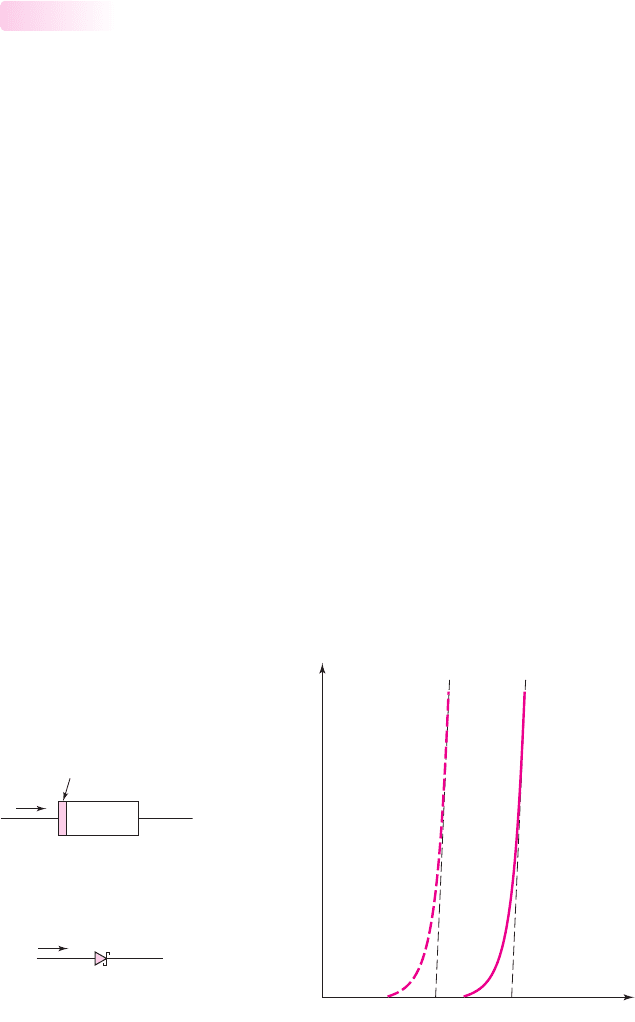
Schottky Barrier Diode
A Schottky barrier diode, or simply a Schottky diode, is formed when a metal, such
as aluminum, is brought into contact with a moderately doped n-type semiconduc-
tor to form a rectifying junction. Figure 1.41(a) shows the metal-semiconductor
contact, and Figure 1.41(b) shows the circuit symbol with the current direction and
voltage polarity.
The current–voltage characteristics of a Schottky diode are very similar to those
of a pn junction diode. The same ideal diode equation can be used for both devices.
However, there are two important differences between the two diodes that directly
affect the response of the Schottky diode.
First, the current mechanism in the two devices is different. The current in a pn
junction diode is controlled by the diffusion of minority carriers. The current in a
Schottky diode results from the flow of majority carriers over the potential barrier at
the metallurgical junction. This means that there is no minority carrier storage in the
Schottky diode, so the switching time from a forward bias to a reverse bias is very
short compared to that of a pn junction diode. The storage time,
t
s
, for a Schottky
diode is essentially zero.
Second, the reverse-saturation current
I
S
for a Schottky diode is larger than that
of a pn junction diode for comparable device areas. This property means that it takes
less forward bias voltage to induce a particular current compared to a pn junction
diode. We will see an application of this in Chapter 17.
Figure 1.42 compares the characteristics of the two diodes. Applying the piece-
wise linear model, we can determine that the Schottky diode has a smaller turn-on
1.5.4
i
D
v
D
V
g
(SB) V
g
(pn)
Schottky
barrier
diode
pn junction
diode
Figure 1.42 Comparison of the forward-bias
I–V characteristics of a pn junction diode and
a Schottky barrier diode
+
–
V
D
I
D
+
Metal
–
V
D
I
D
n -type
(b)
(a)
Figure 1.41 Schottky barrier
diode: (a) simplified geometry
and (b) circuit symbol
nea80644_ch01_07-066.qxd 06/08/2009 05:15 PM Page 50 F506 Tempwork:Dont' Del Rakesh:June:Rakesh 06-08-09:MHDQ134-01 Folder:MHDQ134-01:

Chapter 1 Semiconductor Materials and Diodes 51
voltage than the pn junction diode. In later chapters, we will see how this lower
turn-on voltage and the shorter switching time make the Schottky diode useful in
integrated-circuit applications.
EXAMPLE 1.12
Objective: Determine diode voltages.
The reverse saturation currents of a pn junction diode and a Schottky diode
are
I
S
= 10
−12
A and
10
−8
A, respectively. Determine the forward-bias voltages
required to produce 1 mA in each diode.
Solution: The diode current-voltage relationship is given by
I
D
= I
S
e
V
D
/V
T
Solving for the diode voltage, we obtain
V
D
= V
T
ln
I
D
I
S
We then find, for the pn junction diode
V
D
= (0.026) ln
1 × 10
−3
10
−12
= 0.539 V
and, for the Schottky diode
V
D
= (0.026) ln
1 × 10
−3
10
−8
= 0.299 V
Comment: Since the reverse-saturation current for the Schottky diode is relatively
large, less voltage across this diode is required to produce a given current compared
to the pn junction diode.
EXERCISE PROBLEM
Ex 1.12: A pn junction diode and a Schottky diode both have forward-bias
currents of 1.2 mA. The reverse-saturation current of the pn junction diode is
I
S
= 4 ×10
−15
A. The difference in forward-bias voltages is 0.265 V. Determine
the reverse-saturation current of the Schottky diode. (Ans.
I
S
= 1.07 ×10
−10
A)
Another type of metal–semiconductor junction is also possible. A metal applied
to a heavily doped semiconductor forms, in most cases, an ohmic contact: that is, a
contact that conducts current equally in both directions, with very little voltage drop
across the junction. Ohmic contacts are used to connect one semiconductor device to
another on an IC, or to connect an IC to its external terminals.
Zener Diode
As mentioned earlier in this chapter, the applied reverse-bias voltage cannot increase
without limit. At some point, breakdown occurs and the current in the reverse-bias
1.5.5
nea80644_ch01_07-066.qxd 06/08/2009 05:15 PM Page 51 F506 Tempwork:Dont' Del Rakesh:June:Rakesh 06-08-09:MHDQ134-01 Folder:MHDQ134-01:
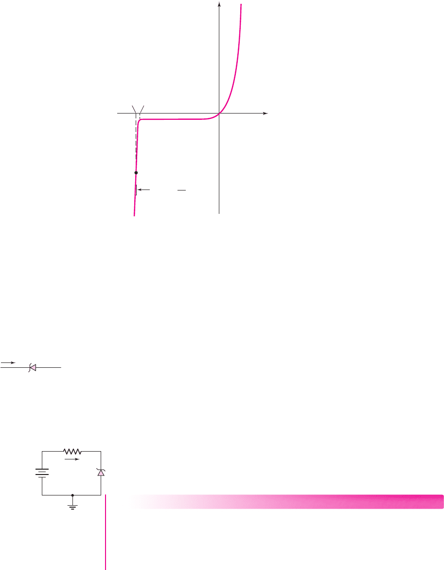
52 Part 1 Semiconductor Devices and Basic Applications
direction increases rapidly. The voltage at this point is called the breakdown voltage.
The diode I–V characteristics, including breakdown, are shown in Figure 1.43.
Diodes, called Zener diodes, can be designed and fabricated to provide a spec-
ified breakdown voltage
V
Zo
. (Although the breakdown voltage is on the negative
voltage axis (reverse-bias), its value is given as a positive quantity.) The large current
that may exist at breakdown can cause heating effects and catastrophic failure of the
diode due to the large power dissipation in the device. However, diodes can be oper-
ated in the breakdown region by limiting the current to a value within the capabilities
of the device. Such a diode can be used as a constant-voltage reference in a circuit.
The diode breakdown voltage is essentially constant over a wide range of currents
and temperatures. The slope of the I–V characteristics curve in breakdown is quite
large, so the incremental resistance
r
z
is small. Typically,
r
z
is in the range of a few
ohms or tens of ohms.
The circuit symbol of the Zener diode is shown in Figure 1.44. (Note the subtle
difference between this symbol and the Schottky diode symbol.) The voltage
V
Z
is
the Zener breakdown voltage, and the current
I
Z
is the reverse-bias current when the
diode is operating in the breakdown region. We will see applications of the Zener
diode in the next chapter.
DESIGN EXAMPLE 1.13
Objective: Consider a simple constant-voltage reference circuit and design the
value of resistance required to limit the current in this circuit.
Consider the circuit shown in Figure 1.45. Assume that the Zener diode break-
down voltage is
V
Z
= 5.6
V and the Zener resistance is
r
z
= 0
. The current in the
diode is to be limited to 3 mA.
Breakdown
voltage
Slope =
1
r
Z
⎜V
Z
⎜
v
D
i
D
⎜V
Zo
⎜
Figure 1.43 Diode I–V characteristics showing breakdown effects
+
–
+
–
V
PS
= 10 V
I
V
Z
= 5.6 V
R
Figure 1.45 Simple circuit
containing a Zener diode in
which the Zener diode is
biased in the breakdown
region
+
–
V
Z
I
Z
Figure 1.44 Circuit symbol
of the Zener diode
nea80644_ch01_07-066.qxd 06/08/2009 05:15 PM Page 52 F506 Tempwork:Dont' Del Rakesh:June:Rakesh 06-08-09:MHDQ134-01 Folder:MHDQ134-01:

Chapter 1 Semiconductor Materials and Diodes 53
Solution: As before, we can determine the current from the voltage difference across
R divided by the resistance. That is,
I =
V
PS
− V
Z
R
The resistance is then
R =
V
PS
− V
Z
I
=
10 − 5.6
3
= 1.47 k
The power dissipated in the Zener diode is
P
Z
= I
Z
V
Z
= (3)(5.6) = 16.8mW
The Zener diode must be able to dissipate 16.8 mW of power without being
damaged.
Comment: The resistance external to the Zener diode limits the current when the
diode is operating in the breakdown region. In the circuit shown in the figure, the out-
put voltage will remain constant at 5.6 V, even though the power supply voltage and
the resistance may change over a limited range. Hence, this circuit provides a con-
stant output voltage. We will see further applications of the Zener diode in the next
chapter.
EXERCISE PROBLEM
Ex 1.13: Consider the circuit shown in Figure 1.45. Determine the value of
resistance R required to limit the power dissipated in the Zener diode to 10 mW.
(Ans.
R = 2.46 k
)
Test Your Understanding
TYU 1.15 Consider the circuit shown in Figure 1.46. The diode can be either a pn
junction diode or a Schottky diode. Assume the cut-in voltages are
V
γ
= 0.7V
and
V
γ
= 0.3V
for the pn junction diode and Schottky diode, respectively. Let
r
f
= 0
for both diodes. Calculate the current
I
D
when each diode is inserted in the circuit.
(Ans. pn diode, 0.825 mA; Schottky diode, 0.925 mA).
TYU 1.16 A Zener diode has an equivalent series resistance of
20
. If the voltage
across the Zener diode is 5.20 V at
I
Z
= 1
mA, determine the voltage across the
diode at
I
Z
= 10
mA. (Ans.
V
Z
= 5.38
V)
TYU 1.17 The resistor in the circuit shown in Figure 1.45 has a value of
R = 4k,
the Zener diode breakdown voltage is
V
Z
= 3.6V,
and the power rating of the Zener
diode is
P = 6.5mW.
Determine the maximum diode current and the maximum
power supply voltage that can be applied without damaging the diode. (Ans. 1.81 mA,
10.8 V).
+
–
V
PS
= 4 V
I
D
Diode
R = 4 kΩ
Figure 1.46 Circuit for
exercise problem TYU 1.15.
The diode can be either a pn
junction diode or a Schottky
diode.
nea80644_ch01_07-066.qxd 06/08/2009 05:15 PM Page 53 F506 Tempwork:Dont' Del Rakesh:June:Rakesh 06-08-09:MHDQ134-01 Folder:MHDQ134-01:

54 Part 1 Semiconductor Devices and Basic Applications
1.6 DESIGN APPLICATION: DIODE THERMOMETER
Objective: • Design a simple electronic thermometer using the tem-
perature characteristics of a diode.
Specifications: The temperature range is to be 0 to
100
◦
F
.
Design Approach: We will use the forward-bias diode temperature characteristics
as shown in Figure 1.20. If the diode current is held constant, the variation in diode
voltage is a function of temperature.
Choices: Assume that a silicon pn junction diode with a reverse-saturation current
of
I
S
= 10
−13
A at
T = 300
K is available.
Solution: Neglecting the
(−1)
term in the diode I–V relation, we have
I
D
= I
S
e
V
D
/V
T
∝ n
2
i
e
V
D
/V
T
∝ e
−E
g
/kT
· e
V
D
/V
T
The reverse-saturation current
I
S
is proportional to
n
2
i
and in turn
n
2
i
is proportional
to the exponential function involving the bandgap energy
E
g
and temperature.
Taking the ratio of the diode current at two temperature values and using the
definition of thermal voltage, we have
3
I
D1
I
D2
=
e
−E
g
/kT
1
· e
eV
D1
/kT
1
e
−E
g
/kT
2
· e
eV
D2
/kT
2
(1.35)
where
V
D1
and
V
D2
are the diode voltages at temperatures
T
1
and
T
2
, respectively. If
the diode current is held constant at the different temperatures, Equation (1.35) can
be written as
e
eV
D2
/kT
2
= e
−E
g
/kT
1
e
+E
g
/kT
2
e
eV
D1
/kT
1
(1.36)
Taking the natural logarithm of both sides, we obtain
eV
D2
kT
2
=
−E
g
kT
1
+
E
g
kT
2
+
eV
D1
kT
1
(1.37)
or
V
D2
=
−E
g
e
T
2
T
1
+
E
g
e
+ V
D1
T
2
T
1
(1.38)
For silicon, the bandgap energy is
E
g
/e = 1.12
V. Then, assuming the bandgap
energy does not vary over the temperature range, we have
V
D2
= 1.12
1 −
T
2
T
1
+ V
D1
T
2
T
1
(1.39)
3
Note that e in, for example,
e
−E
g
/kT
represents the exponential function whereas e in the exponent, for
example,
eV
D1
/kT
1
is the magnitude of the electronic charge. The context in which e is used should make
the meaning clear.
nea80644_ch01_07-066.qxd 06/08/2009 05:15 PM Page 54 F506 Tempwork:Dont' Del Rakesh:June:Rakesh 06-08-09:MHDQ134-01 Folder:MHDQ134-01:

Chapter 1 Semiconductor Materials and Diodes 55
Consider the circuit shown in Figure 1.47. Assume that the diode has a reverse-
saturation current of
I
S
= 10
−13
A at
T = 300
K. From the circuit, we can write
I
D
=
15 − V
D
R
= I
S
e
V
D
/V
T
or
15 − V
D
15 × 10
3
= 10
−13
e
V
D
/0.026
By trial and error, we find
V
D
= 0.5976 V
and
I
D
=
15 − 0.5976
15 × 10
3
⇒ 0.960 mA
In Equation (1.39), we can set
T
1
= 300
K and let
T
2
≡ T
be a variable temper-
ature. We find
V
D
= 1.12 −0.522
T
300
(1.40)
so the diode voltage is a linear function of temperature. If the temperature range is to
be from 0 to
100
◦
F
, for example, the corresponding change in kelvins is from 255.2
to 310.8. The diode voltage versus temperature is plotted in Figure 1.48.
A simple circuit that can be used was shown in Figure 1.47. With a power sup-
ply voltage of 15 V, a change in diode voltage of approximately 0.1 V over the tem-
perature range produces only an approximately 0.67 percent change in diode current.
Thus the preceding analysis is valid.
Comment: This design example shows that a diode connected in a simple circuit
can be used as a sensing element in an electronic thermometer. We assumed a diode
reverse-saturation current of
I
S
= 10
−13
A at
T = 300 K(80
◦
F
). The actual reverse-
saturation current of a particular diode may be different. This difference simply
means that the diode voltage versus temperature curve shown in Figure 1.48 would
slide up or down to match the actual diode voltage at room temperature.
+
–
+
–
15 V
I
D
V
D
R = 15 kΩ
Figure 1.47 Circuit of diode
thermometer
80 60 40 20 0
V
D
(V)
(°F)
(K)
100
0.676
0.598
0.579
255.2 300 310.8
Figure 1.48 Diode voltage versus temperature
nea80644_ch01_07-066.qxd 06/08/2009 05:15 PM Page 55 F506 Tempwork:Dont' Del Rakesh:June:Rakesh 06-08-09:MHDQ134-01 Folder:MHDQ134-01:

56 Part 1 Semiconductor Devices and Basic Applications
Design Pointer: In order to complete this design, two additional components or
electronic systems must be added to the circuit shown in Figure 1.47. First, we must
add a circuit to measure the diode voltage. Adding this circuit must not alter the diode
characteristics and there must be no loading effects. An op-amp circuit that will be
described in Chapter 9 can be used for this purpose. A second electronic system
required is to convert the diode voltage to a temperature reading. An analog-to-digital
converter that will be described in Chapter 16 can be used to provide a digital
temperature reading.
1.7 SUMMARY
• We initially considered some of the characteristics and properties of semicon-
ductor materials, such as the concept of electrons (negative charge) and holes
(positive charge) as two distinct charge carriers in a semiconductor. The doping
process produces either n-type or p-type semiconductor materials. The concepts
of n-type and p-type materials are used throughout the text.
• A pn junction diode is formed when an n-doped region and a p-doped region are
directly adjacent to each other. The diode current is an exponential function of
voltage in the forward-bias condition, and is essentially zero in the reverse-bias
condition.
• A piecewise-linear model of the diode was developed so that approximate hand
calculation results can be easily obtained. The
i − v
characteristics of the diode
are broken into linear segments, which are valid over particular regions of oper-
ation. The concept of a diode turn-on voltage was introduced.
• Time-varying, or ac signals, may be superimposed on a dc diode current and
voltage. A small-signal linear equivalent circuit was developed and is used to
determine the relationship between the ac current and ac voltage. This same
equivalent circuit will be applied extensively when the frequency response of
transistors is discussed.
• Specialized pn junction devices were discussed. In particular, pn junction solar
cells are used to convert solar energy to electrical energy. Schottky barrier diodes
are metal–semiconductor rectifying junctions that, in general, have smaller turn-
on voltages than pn junctions. Zener diodes operate in the reverse breakdown
region and are used in constant-voltage circuits. Photodiodes and LEDs were
also briefly discussed.
• As an application, a simple diode thermometer was designed, based on the tem-
perature properties of the pn junction.
CHECKPOINT
After studying this chapter, the reader should have the ability to:
✓ Understand the concept of intrinsic carrier concentration, the difference between
n-type and p-type materials, and the concept of drift and diffusion currents.
✓ Analyze a simple diode circuit using the ideal diode current–voltage character-
istics and using the iteration analysis technique.
✓ Analyze a diode circuit using the piecewise linear approximation model for the
diode.
nea80644_ch01_07-066.qxd 06/10/2009 07:28 PM Page 56 F506 Tempwork:Dont' Del Rakesh:June:Rakesh 06-10-09:MHDQ134-01:

Chapter 1 Semiconductor Materials and Diodes 57
✓ Determine the small-signal characteristics of a diode using the small-signal
equivalent circuit.
✓ Understand the general characteristics of a solar cell, light-emitting diode,
Schottky barrier diode, and Zener diode.
REVIEW QUESTIONS
1. Describe an intrinsic semiconductor material. What is meant by the intrinsic
carrier concentration?
2. Describe the concept of an electron and a hole as charge carriers in the semicon-
ductor material.
3. Describe an extrinsic semiconductor material. What is the electron concentra-
tion in terms of the donor impurity concentration? What is the hole concentra-
tion in terms of the acceptor impurity concentration?
4. Describe the concepts of drift current and diffusion current in a semiconductor
material.
5. How is a pn junction formed? What is meant by a built-in potential barrier, and
how is it formed?
6. How is a junction capacitance created in a reverse-biased pn junction diode?
7. Write the ideal diode current–voltage relationship. Describe the meaning of
I
S
and
V
T
.
8. Describe the iteration method of analysis and when it must be used to analyze a
diode circuit.
9. Describe the piecewise linear model of a diode and why it is useful. What is the
diode turn-on voltage?
10. Define a load line in a simple diode circuit.
11. Under what conditions is the small-signal model of a diode used in the analysis
of a diode circuit?
12. Describe the operation of a simple solar cell circuit.
13. How do the i–v characteristics of a Schottky barrier diode differ from those of a
pn junction diode?
14. What characteristic of a Zener diode is used in the design of a Zener diode circuit?
15. Describe the characteristics of a photodiode and a photodiode circuit.
PROBLEMS
[Note: Unless otherwise specified, assume that
T = 300 K
in the following prob-
lems. Also, assume the emission coefficient is
n = 1
unless otherwise stated.]
Section 1.1 Semiconductor Materials and Properties
1.1 (a) Calculate the intrinsic carrier concentration in silicon at (i)
T = 250
K
and (ii)
T = 350
K. (b) Repeat part (a) for gallium arsenide.
1.2 (a) The intrinsic carrier concentration in silicon is to be no larger than
n
i
= 10
12
cm
−3
. Determine the maximum allowable temperature. (b) Repeat
part (a) for
n
i
= 10
9
cm
−3
.
1.3 Calculate the intrinsic carrier concentration in silicon and germanium at
(a)
T = 100 K
, (b)
T = 300 K
, and (c)
T = 500 K
.
nea80644_ch01_07-066.qxd 06/10/2009 07:28 PM Page 57 F506 Tempwork:Dont' Del Rakesh:June:Rakesh 06-10-09:MHDQ134-01: