Neamen D. Microelectronics: Circuit Analysis and Design
Подождите немного. Документ загружается.


238 Part 1 Semiconductor Devices and Basic Applications
Table 4.2 is a summary of the small-signal characteristics of the three amplifier
configurations.
The common-source amplifier voltage gain magnitude is generally greater than 1.
The voltage gain of the source follower is slightly less than 1, and that of the
common-gate circuit is generally greater than 1.
The input resistance looking directly into the gate of the common-source and
source-follower circuits is essentially infinite at low to moderate signal frequencies.
However, the input resistance of these discrete amplifiers is the Thevenin equivalent
resistance R
TH
of the bias resistors. In contrast, the input resistance to the common-
gate circuit is generally in the range of only a few hundred ohms.
The output resistance of the source follower is generally in the range of a few
hundred ohms or less. The output resistance of the common-source and common-
gate configurations is dominated by the resistance R
D
. In Chapters 10 and 11, we will
see that the output resistance of these configurations is dominated by the resistance
r
o
when transistors are used as load devices in ICs.
The specific characteristics of these single-stage amplifiers are used in the
design of multistage amplifiers.
4.7 SINGLE-STAGE INTEGRATED
CIRCUIT MOSFET AMPLIFIERS
Objective: • Analyze all-MOS transistor circuits that become the
foundation of integrated circuits.
In the last chapter, we considered three all-MOSFET inverters and plotted the voltage
transfer characteristics. All three inverters use an n-channel enhancement-mode driver
transistor. The three types of load devices are an n-channel enhancement-mode
device, an n-channel depletion-mode device, and a p-channel enhancement-mode de-
vice. The MOS transistor used as a load device is referred to as an active load. We
mentioned that these three circuits can be used as amplifiers.
In this section, we revisit these three circuits and consider their amplifier char-
acteristics. We will emphasize the small-signal equivalent circuits. This section
serves as an introduction to more advanced MOS integrated circuit amplifier designs
considered in Part 2 of the text.
Table 4.2 Characteristics of the three MOSFET amplifier
configurations
Voltage Current Input Output
Configuration gain gain resistance resistance
Common source
A
v
> 1
— R
TH
Moderate to high
Source follower
A
v
∼
=
1
— R
TH
Low
Common gate
A
v
> 1
A
i
∼
=
1
Low Moderate to high
nea80644_ch04_205-284.qxd 06/12/2009 08:00 PM Page 238 F506 Tempwork:Dont' Del Rakesh:June:Rakesh 06-12-09:MHDQ134-04:
Chapter 4 Basic FET Amplifiers 239
Load Line Revisited
In dealing with all-transistor circuits, it will be instructive to consider the equivalent
load lines that we have considered previously in circuits with resistive loads. Before
we deal with the nonlinear load lines or load curves, it may be worthwhile to revisit
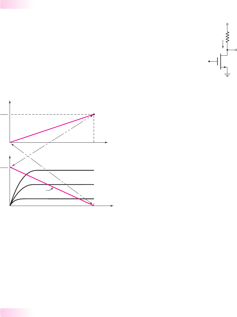
the load line concept of a single transistor with a resistive load.
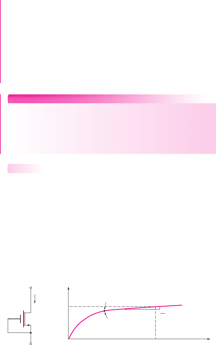
Figure 4.36 shows a single MOSFET with a resistive load. The current–voltage
characteristic of the resistive load device is given by Ohm’s law, or
V
R
= I
D
R
D
. This
curve is plotted in the top portion of Figure 4.37. The load line is given by the KVL
equation around the drain-source loop, or
V
DS
= V
DD
− I
D
R
D
, and is superimposed
on the transistor characteristics in the lower portion of Figure 4.37. We may note that
the last term in the load line equation,
I
D
R
D
, is the voltage across the load device.
4.7.1
V
O
V
DS
V
DD
I
D
V
I
V
R
+
–
+
–
R
D
Figure 4.36 Single
MOSFET circuit with
resistive load
V
D
S
V
DD
V
R
V
DD
V
GS3
V
GS2
V
GS1
Load line
I
D
A'
B'
B
A
V
DD
R
D
I
D
V
DD
R
D
0
0
Load device
Figure 4.37 The I–V curve for the resistor load device (top) and the load line superimposed
on the transistor characteristics (bottom)
We may compare two points on the load device characteristic to the load line.
When
I
D
= 0
,
V
R
= 0
on the load characteristic curve denoted by point A. On the
load line, the
I
D
= 0
point corresponds to
V
DS
= V
DD
, denoted by the point
A
. The
maximum current on the load characteristic curve occurs when
V
R
= V
DD
and is
denoted by point B. On the load line, the maximum current point corresponds to
V
DS
= 0
, denoted by point
B
. The load line can be created by taking the mirror
image of the load characteristic curve and superimposing this curve on the plot of
transistor characteristics. We will see this same effect in the following sections.
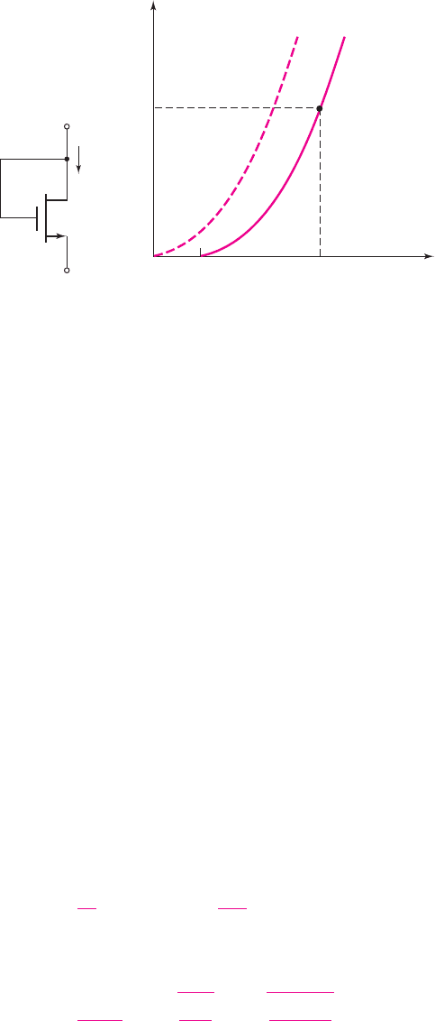
NMOS Amplifiers with Enhancement Load
The characteristics of an n-channel enhancement load device were presented in the last
chapter. Figure 4.38(a) shows an NMOS enhancement load transistor, and Fig-
ure 4.38(b) shows the current–voltage characteristics. The threshold voltage is
V
TNL
.
4.7.2
nea80644_ch04_205-284.qxd 06/12/2009 08:00 PM Page 239 F506 Tempwork:Dont' Del Rakesh:June:Rakesh 06-12-09:MHDQ134-04:
240 Part 1 Semiconductor Devices and Basic Applications
Figure 4.39(a) shows an NMOS amplifier with enhancement load. The driver
transistor is M
D
and the load transistor is M
L
. The characteristics of transistor M
D
and
the load curve are shown in Figure 4.39(b). The load curve is essentially the mirror
image of the i–v characteristic of the load device, as we discussed in the last section.
Since the i–v characteristics of the load device are nonlinear, the load curve is also
nonlinear. The load curve intersects the voltage axis at
V
DD
− V
TNL
, which is the
point where the current in the enhancement load device goes to zero. The transition
point is also shown on the curve.
The voltage transfer characteristic is also useful in visualizing the operation of
the amplifier. This curve is shown in Figure 4.39(c). When the enhancement-mode
driver first begins to conduct, it is biased in the saturation region. For use as an
amplifier, the circuit Q-point should be in this region, as shown in both Fig-
ures 4.39(b) and (c).
We can now apply the small-signal equivalent circuits to find the voltage gain. In
the discussion of the source follower, we found that the equivalent resistance looking
into the source terminal (with
R
S
=∞
) was
R
o
= (1/g
m
)r
o
. The small-signal
equivalent circuit of the inverter is given in Figure 4.40, where the subscripts D and
L refer to the driver and load transistors, respectively. We are again neglecting the
body effect of the load transistor.
The small-signal voltage gain is then
A
v
=
V
o
V
i
=−g
mD
r
oD
1
g
mL
r
oL
(4.49)
Since, generally,
1/g
mL
r
oL
and
1/g
mD
r
oD
, the voltage gain, to a good
approximation is given by
A
v
=
−g
mD
g
mL
=−
K
nD
K
nL
=−
(W/L)
D
(W/L)
L
(4.50)
The voltage gain, then, is related to the size of the two transistors.
(a) (b)
v
D
S
v
DD
V
DS
(sat) = V
GS
– V
TNL
i
D
i
D
(max)
Transistor
characteristics
V
TNL
+
–
v
DS
i
D
Figure 4.38 (a) NMOS enhancement-mode transistor with gate and drain connected in a
load device configuration and (b) current–voltage characteristics of NMOS enhancement
load transistor
nea80644_ch04_205-284.qxd 06/12/2009 08:00 PM Page 240 F506 Tempwork:Dont' Del Rakesh:June:Rakesh 06-12-09:MHDQ134-04:
Chapter 4 Basic FET Amplifiers 241
(c)
(a)
v
GSD
v
O
V
DD
– V
TNL
Transition point
Cutoff point
Q-point
0
V
TND
M
D
cutoff
M
D
in
saturation
M
D
in
nonsaturation
v
DSD
= v
O
V
DD
V
TNL
i
D
i
D
(max)
Q-point
Load curve
Transition point
+
–
v
DSL
+
–
v
GSL
V
DD
i
D
v
O
+
–
v
GSD
M
L
+
–
v
DSD
M
D
v
i
+
–
V
GS
+
–
(b)
Figure 4.39 (a) NMOS amplifier with enhancement load device; (b) driver transistor
characteristics and enhancement load curve with transition point; and (c) voltage transfer
characteristics of NMOS amplifier with enhancement load device
+
–
+
–
V
i
V
gs
r
oD
r
oL
M
L
M
D
V
o
g
mD
V
gs
g
mL
1
Figure 4.40 Small-signal equivalent circuit of NMOS inverter with enhancement load
device
nea80644_ch04_205-284.qxd 06/12/2009 08:00 PM Page 241 F506 Tempwork:Dont' Del Rakesh:June:Rakesh 06-12-09:MHDQ134-04:

242 Part 1 Semiconductor Devices and Basic Applications
DESIGN EXAMPLE 4.11
Objective: Design an NMOS amplifier with an enhancement load to meet a set of
specifications.
Specifications: An NMOS amplifier with the configuration shown in Figure
4.39(a) is to be designed to provide a small-signal voltage gain of
|A
v
|=10
. The
Q-point is to be in the center of the saturation region. The circuit is to be biased at
V
DD
= 5
V.
Choices: NMOS transistors with parameters
V
TN
= 1
V,
k
n
= 60 μA/V
2
, and
λ = 0
are available. The minimum width-to-length ratio is
(W/L)
min
= 1
. Tolerances of
±5
percent in the
k
n
and V
TN
parameters must be considered.
Solution (ac design): From Equation (4.50), we have
|A
v
|=10 =
(W/L)
D
(W/L)
L
which can be written as
W
L
D
= 100
W
L
L
If we set
(W/L)
L
= 1
, then
(W/L)
D
= 100
.
Solution (dc design): Setting the currents in the two transistors equal to each other
(both transistors biased in saturation region), we have
i
DD
= K
nD
(v
GSD
− V
TND
)
2
= i
DL
= K
nL
(v
GSL
− V
TNL
)
2
From Figure 4.39(a), we see that
v
GSL
= V
DD
−v
O
. Substituting, we have
K
nD
(v
GSD
− V
TND
)
2
= K
nL
(V
DD
−v
O
− V
TNL
)
2
Solving for v
O
, we have
v
O
= (V
DD
− V
TNL
) −
K
nD
K
nL
(v
GSD
− V
TND
)
At the transition point,
v
Ot
= v
DSD
(sat) = v
GSDt
− V
TND
where v
GSDt
is the gate-to-source voltage of the driver at the transition point. Then
v
GSDt
− V
TND
= (V
DD
− V
TNL
) −
K
nD
K
nL
(v
GSDt
− V
TND
)
Solving for v
GSDt
, we obtain
v
GSDt
=
(V
DD
− V
TNL
) + V
TND
1 +
K
nD
K
nL
1 +
K
nD
K
nL
Noting that
K
nD
K
nL
=
(W/L)
D
(W/L)
L
= 10
nea80644_ch04_205-284.qxd 06/12/2009 08:00 PM Page 242 F506 Tempwork:Dont' Del Rakesh:June:Rakesh 06-12-09:MHDQ134-04:
Chapter 4 Basic FET Amplifiers 243
we find
v
GSDt
=
(5 − 1) + (1)(1 + 10)
1 + 10
= 1.36 V
and
v
Ot
= v
DSDt
= v
GSDt
− V
TND
= 1.36 −1 = 0.36 V
Considering the transfer characteristics shown in Figure 4.41, we see that the
center of the saturation region is halfway between the cutoff point
(v
GSD
=
V
TND
= 1
V) and the transition point (
v
GSdt
= 1.36
V), or
V
GSQ
=
1.36 − 1.0
2
+1.0 = 1.18 V
Also
V
DSDQ
=
4 − 0.36
2
+0.36 = 2.18 V
Trade-offs: Considering the tolerances in the
k
n
parameter, we find the range in the
small-signal voltage gain to be
|A
v
|
max
=
k
nD
k
nL
·
(W/L)
D
(W/L)
L
=
1.05
0.95
· (100) = 10.5
and
|A
v
|
min
=
k
nD
k
nL
·
(W/L)
D
(W/L)
L
=
0.95
1.05
· (100) = 9.51
V
DSDQ
= 2.18
Transition point
Cutoff point
Q-point
v
O
(V)
v
GSD
(V)
V
GSQ
= 1.18 V
0 1.0 1.2 1.4 1.6
5
4
3
2
1
0.36
1.36 V
Figure 4.41 Voltage transfer characteristics and Q-point of NMOS amplifier with
enhancement load, for Example 4.11
nea80644_ch04_205-284.qxd 06/12/2009 08:00 PM Page 243 F506 Tempwork:Dont' Del Rakesh:June:Rakesh 06-12-09:MHDQ134-04:
244 Part 1 Semiconductor Devices and Basic Applications
The tolerances in the
k
n
and
V
TN
parameters will also affect the Q-point. This analy-
sis is left as an end-of-chapter problem.
Comment: These results show that a very large difference is required in the sizes of
the two transistors to produce a gain of 10. In fact, a gain of 10 is about the largest
practical gain that can be produced by an enhancement load device. A larger small-
signal gain can be obtained by using a depletion-mode MOSFET as a load device, as
shown in the next section.
Design Pointer: The body effect of the load transistor was neglected in this analy-
sis. The body effect will actually lower the small-signal voltage gain from that deter-
mined in the example.
EXERCISE PROBLEM
Ex 4.11: The bias voltage for the enhancement-load amplifier shown in Figure
4.39(a) is
V
DD
= 3.3
V. The transistor parameters are
V
TND
= V
TNL
= 0.4
V,
k
n
= 100 μ
A/V
2
,
(W/L)
L
= 1.2
, and
λ = 0
. (a) Design the circuit such that
the small-signal voltage gain is
|
A
v
|
= 8
. (b) Determine
V
GSDQ
such that the
Q
-point is in the center of the saturation region. (Ans. (a)
(W/L)
D
= 76.8
,
(b)
V
GSDQ
= 0.561
V).
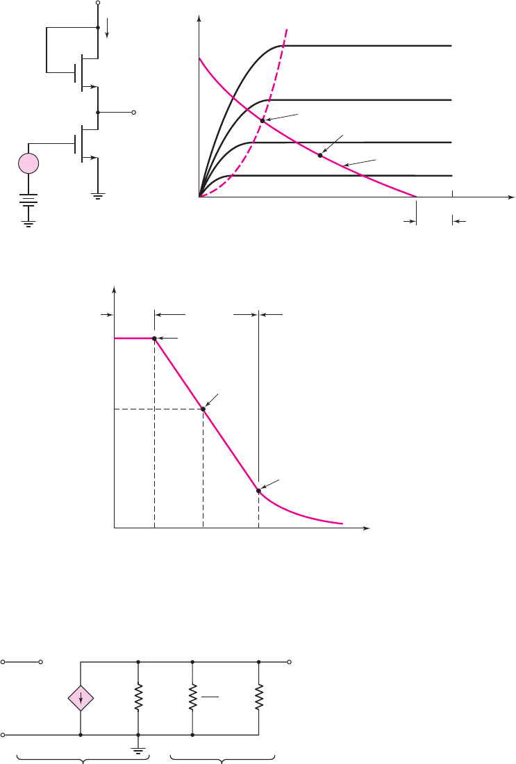
NMOS Amplifier with Depletion Load
Figure 4.42(a) shows the NMOS depletion-mode transistor connected as a load device
and Figure 4.42(b) shows the current–voltage characteristics. The transition point is
also indicated. The threshold voltage V
TNL
of this device is negative, which means that
the v
DS
value at the transition point is positive. Also, the slope of the curve in the
saturation region is not zero; therefore, a finite resistance r
o
exists in this region.
Figure 4.43(a) shows an NMOS depletion load amplifier. The transistor char-
acteristics of M
D
and the load curve for the circuit are shown in Figure 4.43(b). The
load curve, again, is the mirror image of the i–v characteristic of the load device.
Since the i–v characteristics of the load device are nonlinear, the load curve is also
nonlinear. The transition points for both M
D
and M
L
are also indicated. Point A is the
transition point for M
D
, and point B is the transition point for M
L
. The Q-point should
be approximately midway between the two transition points.
4.7.3
(a)
v
DS
v
DD
i
D
i
D
(max)
v
DS
(sat) = –V
TNL
v
GS
= 0
Slope =
1
r
O
Transition
point
(b)
+
–
v
DS
i
D
Flgure 4.42 (a) NMOS depletion-mode transistor with gate and source connected in a load
device configuration and (b) current–voltage characteristic of NMOS depletion load transistor
nea80644_ch04_205-284.qxd 06/12/2009 08:00 PM Page 244 F506 Tempwork:Dont' Del Rakesh:June:Rakesh 06-12-09:MHDQ134-04:
Chapter 4 Basic FET Amplifiers 245
The dc voltage V
GSDQ
biases transistor M
D
in the saturation region at the Q-point.
The signal voltage v
i
superimposes a time-varying gate-to-source voltage on the dc
value, and the bias point moves along the load curve about the Q-point. Again, both
M
D
and M
L
must be biased in their saturation regions at all times.
The voltage transfer characteristic of this circuit is shown in Figure 4.43(c).
Region III corresponds to the condition in which both transistors are biased in the
saturation region. The desired Q-point is indicated.
We can again apply the small-signal equivalent circuit to find the small-signal
voltage gain. Since the gate-to-source voltage of the depletion-load device is held
at zero, the equivalent resistance looking into the source terminal is
R
o
= r
o
.
(c)
Q-point
v
O
v
GSD
I
II
II
III
IV
C
B
A
V
TND
0
V
DD
– ⎜V
TNL
⎜
V
DD
(a)
+
–
V
DD
i
D
v
O
+
–
M
D
v
DSD
v
i
+
–
V
GSDQ
M
L
v
DSL
+
–
v
DSD
V
GSD
V
DD
i
D
i
D
(max)
Q-point
Load curve
B
C
A
(b)
Figure 4.43 (a) NMOS amplifier with depletion load device; (b) driver transistor
characteristics and depletion load curve, with transition points between saturation and
nonsaturation regions; (c) voltage transfer characteristics
nea80644_ch04_205-284.qxd 06/12/2009 08:00 PM Page 245 F506 Tempwork:Dont' Del Rakesh:June:Rakesh 06-12-09:MHDQ134-04:
246 Part 1 Semiconductor Devices and Basic Applications
+
–
V
i
+
–
V
gs
M
D
M
L
V
o
r
oL
r
oD
g
mD
V
gs
Figure 4.44 Small-signal equivalent circuit of NMOS inverter with depletion load device
The small-signal equivalent circuit of the inverter is given in Figure 4.44, where
the subscripts D and L refer to the driver and load transistors, respectively. We are
again neglecting the body effect of the load device.
The small-signal voltage gain is then
A
v
=
V
o
V
i
=−g
mD
(r
oD
r
oL
)
(4.51)
In this circuit, the voltage gain is directly proportional to the output resistances of the
two transistors.
EXAMPLE 4.12
Objective: Determine the small-signal voltage gain of the NMOS amplifier with
depletion load.
For the circuit shown in Figure 4.43(a), assume transistor parameters of
V
TND
=+0.8
V,
V
TNL
=−1.5
V,
K
nD
= 1
mA/V
2
,
K
nL
= 0.2
mA/V
2
, and
λ
D
=
λ
L
= 0.01 V
−1
. Assume the transistors are biased at
I
DQ
= 0.2
mA.
Solution: The transconductance of the driver is
g
mD
= 2
K
nD
I
DQ
= 2
(1)(0.2) = 0.894 mA/V
Since
λ
D
= λ
L
, the output resistances are
r
oD
= r
oL
=
1
λI
DQ
=
1
(0.01)(0.2)
= 500 k
The small-signal voltage gain is then
A
v
=−g
mD
(r
oD
r
oL
) =−(0.894)(500500) =−224
Comment: The voltage gain of the NMOS amplifier with depletion load is, in
general, significantly larger than that with the enhancement load device. The body
effect will lower the ideal gain factor.
Discussion: One aspect of this circuit design that we have not emphasized is the
dc biasing. We mentioned that both transistors need to be biased in their saturation
regions. From Figure 4.43(a), this dc biasing is accomplished with the dc source
V
GSDQ
. However, because of the steep slope of the transfer characteristics (Fig-
ure 4.43(c)), applying the “correct” voltage becomes difficult. As we will see in the
next section, dc biasing is generally accomplished with current source biasing.
nea80644_ch04_205-284.qxd 06/12/2009 08:00 PM Page 246 F506 Tempwork:Dont' Del Rakesh:June:Rakesh 06-12-09:MHDQ134-04:
Chapter 4 Basic FET Amplifiers 247
EXERCISE PROBLEM
Ex 4.12: Assume the depletion-load amplifier in Figure 4.43(a) is biased at
I
DQ
= 0.1
mA. The transistor parameters are
K
nD
= 250 μ
A/V
2
,
K
nL
=
25 μ
A/V
2
,
V
TND
= 0.4
V,
V
TNL
=−0.8
V, and
λ
1
= λ
2
= 0.02
V
−1
. Determine
the small-signal voltage gain. (Ans.
A
v
=−79.1)
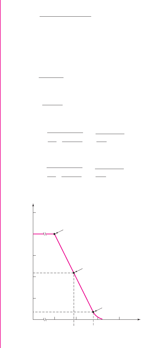
NMOS Amplifier with Active Loads
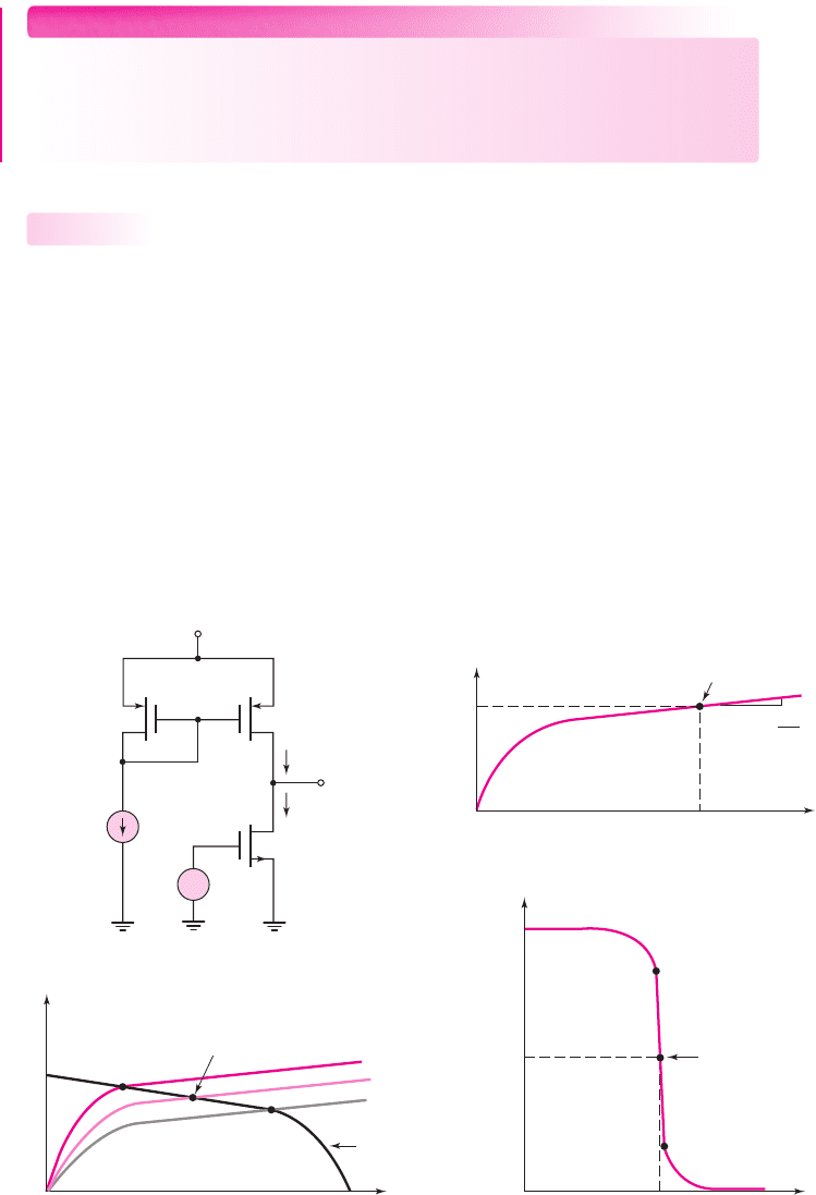
CMOS Common-Source Amplifier
An amplifier using an n-channel enhancement-mode driver and a p-channel
enhancement mode active load is shown in Figure 4.45(a) in a common-source
configuration. The p-channel active load transistor M
2
is biased from M
3
and I
Bias
.
This configuration is similar to the MOSFET current source shown in Figure 3.49 in
Chapter 3. With both n- and p-channel transistors in the same circuit, this circuit is
now referred to as a CMOS amplifier. The CMOS configuration is used almost
exclusively rather than the NMOS enhancement load or depletion load devices.
The i–v characteristic curve for M
2
is shown in Figure 4.45(b). The source-to-
gate voltage is a constant and is established by M
3
. The driver transistor characteris-
tics and the load curve are shown in Figure 4.45(c). The transition points of both M
1
4.7.4
I
Bias
Q-point
i
2
v
SG2
= V
S
G
v
SD2
slope =
1
r
op
(b)
Q-point
Q-point
Load
curve
i
1
V
DD
A
B
v
DS1
(c)
v
O
V
DD
A
B
v
1
(d)
+
–
V
DD
M
3
I
Bias
v
I
i
2
i
1
M
2
M
1
V
SG
v
o
+
–
v
SD2
+
–
v
DS1
+
–
(a)
Figure 4.45 (a) CMOS common-source amplifier; (b) PMOS active load i–v characteristic,
(c) driver transistor characteristics with load curve, (d) voltage transfer characteristics
nea80644_ch04_205-284.qxd 06/12/2009 08:00 PM Page 247 F506 Tempwork:Dont' Del Rakesh:June:Rakesh 06-12-09:MHDQ134-04: