Neamen D. Microelectronics: Circuit Analysis and Design
Подождите немного. Документ загружается.

358 Part 1 Semiconductor Devices and Basic Applications
5.34 (a) The transistor shown in Figure P5.34 has
β = 100
. Determine
V
O
for
(i)
I
Q
= 0.1
mA, (ii)
I
Q
= 0.5
mA, and (iii)
I
Q
= 2
mA. (b) Determine the
percent change in
V
O
for the conditions in part (a) if the current gain
increases to
β = 150
.
5.35 Assume
β = 120
for the transistor in the circuit shown in Figure P5.34.
Determine
I
Q
such that (a)
V
O
= 4
V, (b)
V
O
= 2
V, and (c)
V
O
= 0
.
5.36 For the circuit shown in Figure P5.27, calculate and plot the power
dissipated in the transistor for
I
Q
=
0, 0.5, 1.0, 1.5, 2.0, 2.5, and 3.0 mA.
Assume
β = 50
.
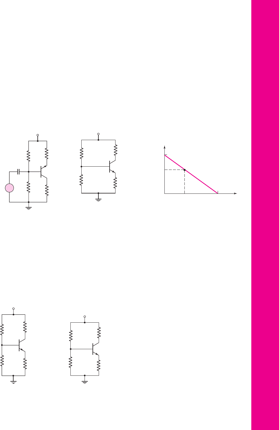
5.37 Consider the common-base circuit shown in Figure P5.37. Assume the tran-
sistor alpha is
α = 0.9920
. Determine
I
E
,
I
C
,and
V
BC
.
D5.40 (a) The circuit shown in Figure P5.40 is to be designed such that
I
CQ
=
0.5 mA and
V
CEQ
= 2.5
V. Assume
β = 120
. Sketch the load line and plot
the Q-point. (b) Pick standard values of resistors that are close to the
designed values. Assume that the standard resistor values vary by
±10
R
1
= 15 kΩ
R
2
= 100 kΩ
R
C
= 2.2 kΩ
V
CC
= 12 V
–12 V
V
1
Figure P5.38
R
1
= 15 kΩ
R
2
= 100 kΩ
R
C
= 1 kΩ
V
CC
= 5 V
–5 V
V
1
+
–
V
CE
Figure P5.39
R
B
R
C
V
CC
= 5 V
Figure P5.40
+
–
+
+
–
–
V
EE
= 9 V
V
CC
= 9 V
V
BC
R
C
= 2.2 kΩ
R
E
= 4 kΩ
Figure P5.37
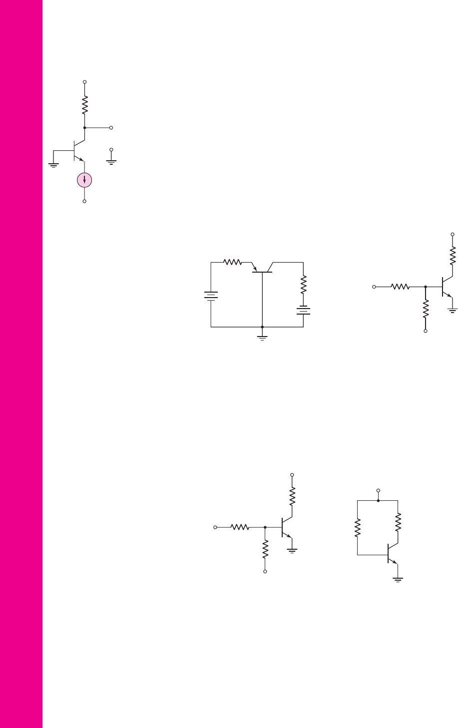
5.38 (a) For the transistor in Figure P5.38,
β = 80
. Determine
V
1
such that
V
CEQ
= 6
V. (b) Determine the range in
V
1
that produces
3 ≤ V
CEQ
≤ 9
V.
5.39 Let
β = 25
for the transistor in the circuit shown in Figure P5.39. Deter-
mine the range of
V
1
such that
1.0 ≤ V
CE
≤ 4.5
V. Sketch the load line and
show the range of the Q-point values.
R
C
= 5 kΩ
V
O
I
Q
+5 V
–5 V
+
–
Figure P5.34
nea80644_ch05_285-368.qxd 06/12/2009 08:43 PM Page 358 F506 Tempwork:Dont' Del Rakesh:June:Rakesh 06-12-09:MHDQ134-05:

percent. Plot the load lines and Q-point values for the maximum and mini-
mum values of
R
B
and
R
C
values (four Q-point values).
5.41 The circuit shown in Figure P5.41 is sometimes used as a thermometer.
Assume the transistors
Q
1
and
Q
2
in the circuit are identical. Writing the
emitter currents in the form
I
E
= I
EO
exp(V
BE
/V
T
)
, derive the expression
for the output voltage
V
O
as a function of temperature T.
Chapter 5 The Bipolar Junction Transistor 359
5.42 The transistor in Figure P5.42 has
β = 120
. (a) Determine
V
I
that produces
V
O
= 4
V for (i)
R
E
= 0
and (ii)
R
E
= 1
k
. (b) Repeat part (a) for
V
O
= 2.5
V. (c) Determine
V
O
for
V
I
= 3.5
V and for
R
E
= 1
k
.
5.43 The common-emitter current gain of the transistor in Figure P5.43 is
β = 80
.
Plot the voltage transfer characteristics over the range
0 ≤ V
I
≤ 5
V.
V
CC
= 5 V
10 I
I
Q
2
Q
1
V
O
–
+
Figure P5.41
5.44 For the circuit shown in Figure P5.44, plot the voltage transfer characteris-
tics over the range
0 ≤ V
I
≤ 5
V. Assume
β = 100
.
Section 5.3 Basic Transistor Applications
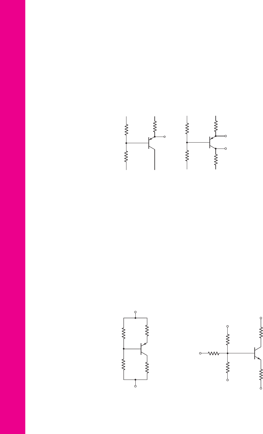
5.45 The transistor in the circuit shown in Figure P5.45 has a current gain
of
β = 40
. Determine
R
B
such that
V
O
= 0.2
V and
I
C
/I
B
= 20
when
V
I
= 5
V.
V
O
R
E
+5 V
V
I
R
C
= 4 kΩ
R
B
= 200 kΩ
Figure P5.42
V
O
+5 V
V
I
R
C
= 4 kΩ
R
B
= 180 kΩ
Figure P5.43
V
O
+5 V
V
I
R
C
= 4 kΩ
R
E
= 1 kΩ
R
B
= 180 kΩ
Figure P5.44
Figure P5.45
V
CC
= 5 V
V
O
V
I
R
C
= 200 Ω
R
B
nea80644_ch05_285-368.qxd 06/12/2009 08:43 PM Page 359 F506 Tempwork:Dont' Del Rakesh:June:Rakesh 06-12-09:MHDQ134-05:
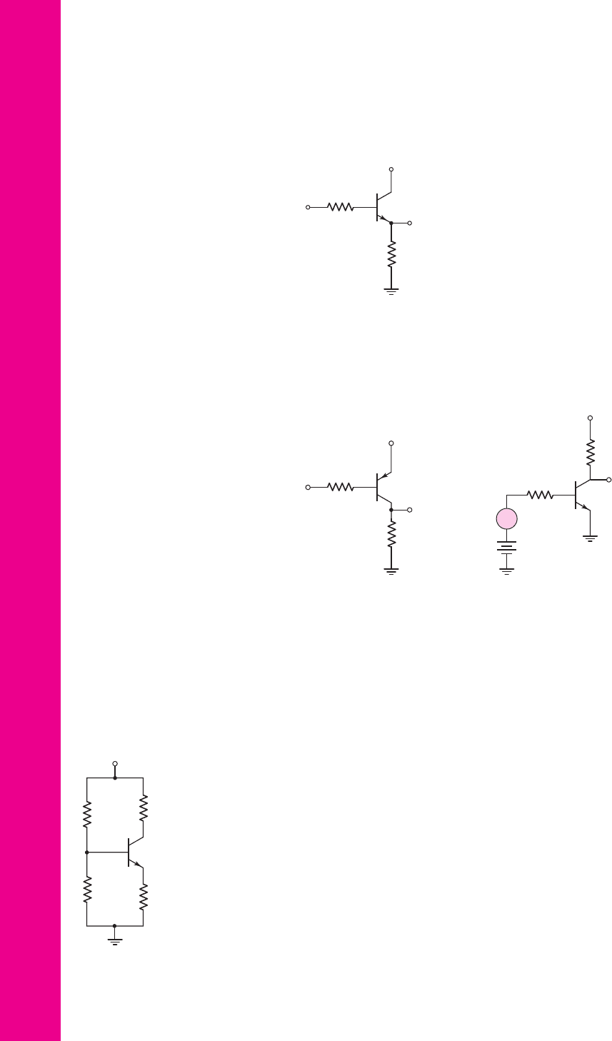
360 Part 1 Semiconductor Devices and Basic Applications
5.46 Consider the circuit in Figure P5.46. For the transistor,
β = 50
. Find
I
B
,
I
C
,
I
E
, and
V
O
for (a)
V
I
= 0
, (b)
V
I
= 2.5
V, and (c)
V
I
= 5
V.
5.48 Consider the amplifier circuit shown in Figure P5.48. Assume a transis-
tor current gain of
β = 120
. The voltage
V
BB
establishes the
Q
-point,
and the voltage
υ
i
is a time-varying signal that produces a variation in the
base current, which in turn produces a variation in the collector current
and hence a variation in the output voltage
v
o
. (a) Determine
R
B
such that
V
CEQ
= 1.6
V. (b) Determine the maximum variation in the output volt-
age such that the transistor does not enter cutoff or saturation. (c) What is
the voltage gain
v
o
/v
i
of the amplifier? (d) What is the maximum
variation in the voltage
v
i
such that the transistor does not enter cutoff or
saturation?
Section 5.4 Bipolar Transistor Biasing
D5.49 For the transistor in the circuit shown in Figure P5.49, assume
β = 120
.
Design the circuit such that
I
CQ
= 0.15
mA and
R
TH
= 200
k
. What is
the value of
V
CEQ
?
5.50 Reconsider Figure P5.49. The transistor current gain is
β = 150
. The circuit
parameters are changed to
R
TH
= 120
k
and
R
E
= 1
k
. Determine the
values of
R
C
,
R
1
, and
R
2
such that
V
CEQ
= 1.5
V and
I
CQ
= 0.20
mA.
5.51 The current gain of the transistor shown in the circuit of Figure P5.51 is
β = 100
. Determine
V
B
and
I
EQ
.
Figure P5.46
Figure P5.47 Figure P5.48
V
O
V
I
R
E
= 500 Ω
V
CC
= 3 V
R
B
= 10 kΩ
V
O
V
+
= 9 V
V
I
R
C
= 500 Ω
R
B
Figure P5.49
R
C
= 2 kΩ
R
B
V
CC
= 3 V
V
BB
=
1.0 V
v
i
+
–
+
–
V
O
R
C
=
6 kΩ
R
E
=
2 kΩ
R
2
R
1
V
CC
= 2.5 V
V
B
5.47 The current gain for the transistor in the circuit in Figure P5.47 is
β = 60
.
Determine
R
B
such that
V
O
= 8.8
V when
V
I
= 5
V and
I
C
/I
B
= 25
.
nea80644_ch05_285-368.qxd 06/12/2009 08:43 PM Page 360 F506 Tempwork:Dont' Del Rakesh:June:Rakesh 06-12-09:MHDQ134-05:
Chapter 5 The Bipolar Junction Transistor 361
+5 V
–5 V
R
2
= 2 kΩ
R
E
= 0.5 kΩ
R
1
= 12 kΩ
R
C
= 5 kΩ
C
C
v
s
+
–
Figure P5.55
5.52 For the circuit shown in Figure P5.52, let
β = 125
. (a) Find
I
CQ
and
V
CEQ
.
Sketch the load line and plot the Q-point. (b) If the resistors
R
1
and
R
2
vary
by
±5
percent, determine the range in
I
CQ
and
V
CEQ
. Plot the various
Q-points on the load line.
5.53 Consider the circuit shown in Figure P5.53. (a) Determine
I
BQ
,
I
CQ
, and
V
CEQ
for
β = 80
. (b) What is the percent change in
I
CQ
and
V
CEQ
if
β
is
changed to
β = 120
?
5.54 (a) Redesign the circuit shown in Figure P5.49 using
V
CC
= 9
V such
that the voltage drop across
R
C
is
(
1
3
)V
CC
and the voltage drop across
R
E
is
(
1
3
)V
CC
. Assume
β = 100
. The quiescent collector current is to be
I
CQ
=
0.4 mA, and the current through
R
1
and
R
2
should be approximately
0.2I
CQ
. (b) Replace each resistor in part (a) with the closest standard value
(Appendix C). What is the value of
I
CQ
and what are the voltage drops
across
R
C
and
R
E
?
5.55 For the circuit shown in Figure P5.55, let
β = 100
. (a) Find
R
TH
and
V
TH
for the base circuit. (b) Determine
I
CQ
and
V
CEQ
. (c) Draw the load line and
plot the Q-point. (d) If the resistors
R
C
and
R
E
vary by
±5
percent, deter-
mine the range in
I
CQ
and
V
CEQ
. Draw the load lines corresponding to the
maximum and minimum resistor values and plot the Q-points.
5.56 Consider the circuit shown in Figure P5.56. (a) Determine
R
TH
,
V
TH
,
I
BQ
,
I
CQ
, and
V
ECQ
for
β = 90
. (b) Determine the percent change in
I
CQ
and
V
ECQ
if
β
is changed to
β = 150
.
C
C
v
i
V
CC
= 24 V
R
2
= 42 kΩ
R
E
= 10 kΩ
R
1
= 58 kΩ
+
–
R
C
=
5.25 kΩ
R
1
=
96 kΩ
R
2
=
24 kΩ
R
E
=
1 kΩ
V
CC
= 9 V
Figure P5.52
Figure P5.53
Figure P5.51
V
CC
= +10 V
R
E
= 1 kΩ
R
1
= 20 kΩ
R
2
= 15 kΩ
V
B
I
EQ
Figure P5.56
R
E
=
0.7 kΩ
R
1
=
40 kΩ
R
2
=
40 kΩ
R
C
=
1.6 kΩ
V
+
= 2.5 V
nea80644_ch05_285-368.qxd 06/12/2009 08:43 PM Page 361 F506 Tempwork:Dont' Del Rakesh:June:Rakesh 06-12-09:MHDQ134-05:
362 Part 1 Semiconductor Devices and Basic Applications
v
s
R
1
C
C
R
E
= 200 Ω
R
2
+
–
V
+
= +6 V
V
–
= –6 V
R
C
= 2 kΩ
Figure P5.61
5.57 (a) Determine the Q-point values for the circuit in Figure P5.57. Assume
β = 50
. (b) Repeat part (a) if all resistor values are reduced by a factor of 3.
(c) Sketch the load lines and plot the Q-point values for parts (a) and (b).
5.58 (a) Determine the Q-point values for the circuit in Figure P5.58. Assume
β = 50
. (b) Repeat part (a) if all resistor values are reduced by a factor of 3.
(c) Sketch the load lines and plot the Q-point values for parts (a) and (b).
D5.59 (a) For the circuit shown in Figure P5.59, design a bias-stable circuit such
that
I
CQ
= 0.8
mA and
V
CEQ
= 5
V. Let
β = 100
. (b) Using the results of
part (a), determine the percentage change in
I
CQ
if
β
is in the range
75 ≤ β ≤ 150
. (c) Repeat parts (a) and (b) if
R
E
= 1
k
.
D5.60 Design a bias-stable circuit in the form of Figure P5.59 with
β = 120
such
that
I
CQ
= 0.8
mA,
V
CEQ
= 5
V, and the voltage across
R
E
is approxi-
mately 0.7 V.
D5.61 Using the circuit in Figure P5.61, design a bias-stable amplifier such that
the Q-point is in the center of the load line. Let
β = 125
. Determine
I
CQ
,
V
CEQ
,
R
1
, and
R
2
.
D5.62 For the circuit shown in Figure P5.61, the bias voltages are changed to
V
+
= 3
V and
V
−
=−3
V. (a) Design a bias-stable circuit for
β = 120
R
1
=
68 kΩ
R
C
=
42 kΩ
R
E
=
30 kΩ
R
2
=
36 kΩ
V
CC
= 10 V
Figure P5.57
R
1
=
36 kΩ
R
E
=
30 kΩ
R
C
=
42 kΩ
R
2
=
68 kΩ
V
+
= +5 V
V
–
= – 5 V
Figure P5.58
v
s
C
C1
C
C2
C
E
V
CC
= 10 V
R
2
R
1
R
E
= 0.5 kΩ
R
L
= 1 kΩ
R
C
+
–
Figure P5.59
nea80644_ch05_285-368.qxd 06/12/2009 08:43 PM Page 362 F506 Tempwork:Dont' Del Rakesh:June:Rakesh 06-12-09:MHDQ134-05:
Chapter 5 The Bipolar Junction Transistor 363
such that
V
CEQ
= 2.8
V. Determine
I
CQ
,
R
1
, and
R
2
. (b) If the resistors
R
1
and
R
2
vary by
±5
percent, determine the range in
I
CQ
and
V
CEQ
. Plot the
various
Q
-points on the load line.
5.63 (a) A bias-stable circuit with the configuration shown in Figure P5.61 is to
be designed such that
I
CQ
= (3 ±0.1)
mA and
V
CEQ
∼
=
5
V using a tran-
sistor with
75 ≤ β ≤ 150
. (b) Sketch the load line and plot the range of
Q-point values for part (a).
D5.64 (a) For the circuit shown in Figure P5.64, assume that the transistor current
gain is
β = 90
and that the circuit parameter is
R
TH
= 2.4
k
. Design the
circuit such that
V
ECQ
= 1.5
V. Find
I
BQ
,
I
CQ
,
R
1
, and
R
2
. (b) Determine
the values of
I
BQ
,
I
CQ
, and
V
ECQ
if the current gain is changed to
β = 130
.
R
1
R
E
R
2
V
CC
= 18 V
R
C
= 2 kΩ
(a)
6180
4.8
7.2
v
CE
(V)
i
C
(mA)
Q-point
(b)
Figure P5.65Figure P5.64
5.65 The dc load line and Q-point of the circuit in Figure P5.65(a) are shown in
Figure P5.65(b). For the transistor,
β = 120
. Find
R
E
,
R
1
, and
R
2
such that
the circuit is bias stable.
D5.66 The range of
β
for the transistor in the circuit in Figure P5.66 is
80 ≤ β ≤ 120
. Design a bias-stable circuit such that the nominal Q-point
values are
I
CQ
= 0.2
mA and
V
CEQ
= 1.6
V. The value of
I
CQ
must fall in
the range
0.19 ≤ I
CQ
≤ 0.21
mA. Determine
R
E
,
R
1
, and
R
2
.
D5.67 The nominal Q-point of the circuit in Figure P5.67 is
I
CQ
= 1
mA and
V
CEQ
= 5
V, for
β = 60
. The current gain of the transistor is in the range
Figure P5.66
C
C
R
E
=
2 kΩ
v
i
R
2
R
1
+
–
R
C
=
1 kΩ
V
+
= 3.3 V
R
C
=
4 kΩ
R
1
R
2
R
E
V
CC
= 2.5 V
R
1
R
E
R
2
V
CC
= 15 V
R
C
= 5 kΩ
Figure P5.67
nea80644_ch05_285-368.qxd 06/12/2009 08:43 PM Page 363 F506 Tempwork:Dont' Del Rakesh:June:Rakesh 06-12-09:MHDQ134-05:
364 Part 1 Semiconductor Devices and Basic Applications
45 ≤ β ≤ 75
. Design a bias-stable circuit such that
I
CQ
does not vary by
more than 5 percent from its nominal value.
D5.68 (a) For the circuit in Figure P5.67, the value of
V
CC
is changed to 3 V. Let
R
C
= 5
R
E
and
β = 120
. Redesign a bias-stable circuit such that
I
CQ
=
100
μ
A and
V
CEQ
= 1.4
V. (b) Using the results of part (a), determine the
dc power dissipation in the circuit.
D5.69 For the circuit in Figure P5.69, let
β = 100
and
R
E
= 3
k
. Design a bias-
stable circuit such that
V
E
= 0
.
5.70 For the circuit in Figure P5.70, let
R
C
= 2.2
k
,
R
E
= 2
k
,
R
1
= 10
k
,
R
2
= 20
k
, and
β = 60
. (a) Find
R
TH
and
V
TH
for the base circuit.
(b) Determine
I
BQ
,
I
CQ
,
V
E
, and
V
C
.
D5.71 Design the circuit in Figure P5.70 to be bias stable and to provide nominal
Q-point values of
I
CQ
= 0.5
mA and
V
ECQ
= 8
V. Let
β = 60
. The maxi-
mum current in
R
1
and
R
2
is to be limited to 40
μ
A.
D5.72 Consider the circuit shown in Figure P5.72. (a) The nominal transistor cur-
rent gain is
β = 80
. Design a bias-stable circuit such that
I
CQ
= 0.15
mA
and
V
ECQ
= 2.7
V. (b) Using the results of part (a), determine the percent
change in
I
CQ
and
V
ECQ
if the transistor current gain is in the range
60 ≤ β ≤ 100
.
5.73 For the circuit in Figure P5.73, let
β = 100
. (a) Find
V
TH
and
R
TH
for the
base circuit. (b) Determine
I
CQ
and
V
CEQ
.
R
1
R
2
+5 V+2 V
–5 V–2 V
R
E
V
E
Figure P5.69
R
1
R
2
R
C
R
E
+5 V +10 V
– 5 V –10 V
V
E
V
C
Figure P5.70
R
E
=
2 kΩ
R
1
R
2
R
C
V
+
= 2.5 V
V
= –2.5 V
–
500 kΩ
500 kΩ
70 kΩ
50 kΩ
5 kΩ
–5 V
–5 V
+15 V
+5 V
+3 V
Figure P5.73Figure P5.72
nea80644_ch05_285-368.qxd 06/12/2009 08:43 PM Page 364 F506 Tempwork:Dont' Del Rakesh:June:Rakesh 06-12-09:MHDQ134-05:

Chapter 5 The Bipolar Junction Transistor 365
D5.74 Design a bias-stable four-resistor bias network for an npn transistor such
that
I
CQ
= 0.8
mA,
V
CEQ
= 4
V, and
V
E
= 1.5
V. The circuit and transistor
parameters are
V
CC
= 10
V and
β = 120
, respectively.
D5.75 (a) Design a four-resistor bias network with the configuration shown in Fig-
ure P5.61 to yield Q-point values of
I
CQ
= 50 μ
A and
V
CEQ
= 5
V. The
bias voltages are
V
+
=+5
V and
V
−
=−5V
. Assume a transistor with
β = 80
is available. The voltage across the emitter resistor should be
approximately 1 V. (b) The transistor in part (a) is replaced by one with
β = 120
. Determine the resulting Q-point.
D5.76 (a) Design a four-resistor bias network with the configuration shown in Fig-
ure P5.61 to yield
Q
-point values of
I
CQ
= 0.50
mA and
V
CEQ
= 2.5
V. The
bias voltages are
V
+
= 3V
and
V
−
=−3
V. The transistor current gain is
β = 120
. The voltage across the emitter resistor should be approximately 0.7
V. (b) Replace the designed resistors in part (a) with standard resistors with
values closest to the designed values. Determine the resulting
Q
-point.
D5.77 (a) A four-resistor bias network is to be designed with the configuration
shown in Figure P5.77. The
Q
-point values are to be
I
CQ
= 100 μ
A and
V
ECQ
= 3
V. The bias voltages are
V
+
= 3
V and
V
−
=−3
V. A transistor
with
β = 110
is available. The voltage across the emitter resistor should be
approximately 0.7 V. (b) The transistor in part (a) is replaced with one with
β = 150
. What is the resulting
Q
-point?
D5.78 (a) Design a four-resistor bias network with the configuration shown in Fig-
ure P5.77 such that the Q-point values are
I
CQ
= 1.2
mA and
V
ECQ
= 6
V.
The bias voltages are
V
+
= 9
V and
V
−
=−9
V. A transistor with
β = 75
is available. The voltage across the emitter resistor should be approximately
1.5 V. (b) Replace the designed resistors in part (a) with standard resistors
with values closest to the designed values. Determine the resulting Q-point.
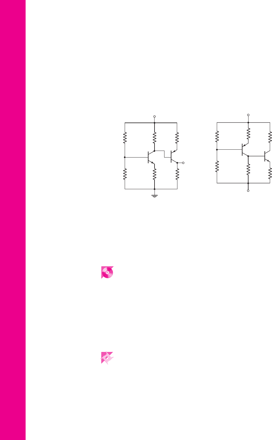
Section 5.5 Multistage Circuits
5.79 For each transistor in the circuit in Figure P5.79,
β = 120
and the B–E turn-
on voltage is 0.7 V. Determine the quiescent base, collector, and emitter cur-
rents in
Q
1
and
Q
2
. Also determine
V
CEQ1
and
V
CEQ2
.
5.80 The parameters for each transistor in the circuit in Figure P5.80 are
β = 80
and
V
BE
(on) = 0.7
V. Determine the quiescent values of base, collector, and
emitter currents in
Q
1
and
Q
2
.
R
1
R
2
R
C
R
E
V
+
V
–
Figure P5.77
R
1
= 100 kΩ
R
C1
=
3 kΩ
R
E 2
= 5 kΩ
R
E1
=
1 kΩ
+10 V
–10 V
R
2
=
40 kΩ
Q
2
Q
1
C
C
v
s
v
O
+
–
Figure P5.79
R
E2
= 1 kΩ
R
E1
= 20 kΩ
+5 V
–5 V
Q
1
Q
2
Figure P5.80
nea80644_ch05_285-368.qxd 06/12/2009 08:43 PM Page 365 F506 Tempwork:Dont' Del Rakesh:June:Rakesh 06-12-09:MHDQ134-05:
366 Part 1 Semiconductor Devices and Basic Applications
D5.81 The bias voltage in the circuit shown in Figure 5.63 is changed to
V
+
= 5
V. Design the circuit to meet the following specifications:
V
CE1
= V
CE2
= 1.2
V,
V
RE
= 0.5
V,
I
C1
∼
=
I
C2
∼
=
0.2
mA, and
I
R1
∼
=
I
R2
∼
=
I
R3
∼
=
20 μ
A.
5.82 Consider the circuit shown in Figure P5.82. The current gain for the npn
transistor is
β
n
= 120
and for the pnp transistor is
β
p
= 80
. Determine
I
B1
,
I
C1
,
I
B2
,
I
C2
,
V
CE1
, and
V
EC2
.
5.83 (a) For the transistors in the circuit shown in Figure P5.83, the parameters
are:
β = 100
and
V
BE
(on) = V
EB
(on) = 0.7
V. Determine
R
C1
,
R
E1
,
R
C2
,
and
R
E2
such that
I
C1
= I
C2
= 0.8
mA,
V
ECQ1
= 3.5
V, and
V
CEQ2
=
4.0 V. (b) Correlate the results of part (a) with a computer simulation.
COMPUTER SIMULATION PROBLEMS
5.84 Using a computer simulation, plot
V
CE
versus
V
1
over the range
0 ≤ V
I
≤ 8
V
for the circuit in Figure 5.24(a). At what voltage does the transistor turn on
and at what voltage does the transistor go into saturation?
5.85 Using a computer simulation, verify the results of Example 5.7.
5.86 Consider the circuit and parameters in Example 5.15. Using a computer
simulation, determine the change in Q-point values if all resistors vary by
±5
percent.
5.87 Using a computer simulation, verify the results of Example 5.19.
DESIGN PROBLEMS
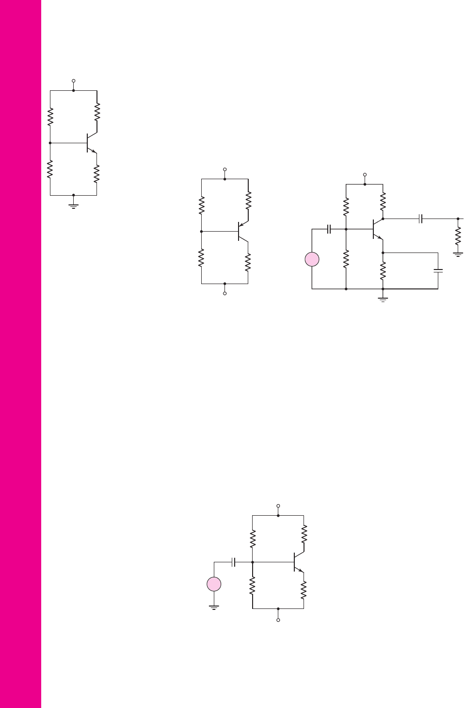
[Note: Each design should be correlated with a computer simulation.]
*D5.88 Consider a common-emitter circuit with the configuration shown in Figure
5.54(a). Assume a bias voltage of
V
CC
= 3.3
V and assume the transistor
current gain is in the range
100 ≤ β ≤ 160
. Design the circuit such that the
nominal Q-point is in the center of the load line and that the Q-point values
R
E2
R
C1
–5 V
+5 V
R
E1
R
C2
R
2
= 100 kΩ
R
1
= 50 kΩ
Q
1
Q
2
Figure P5.83Figure P5.82
80 kΩ
2 kΩ
100 Ω
200 Ω
Q
1
Q
2
2 kΩ
40 kΩ
V
+
= 9 V
V
O
nea80644_ch05_285-368.qxd 06/12/2009 08:43 PM Page 366 F506 Tempwork:Dont' Del Rakesh:June:Rakesh 06-12-09:MHDQ134-05:

do not vary by more than
±3
percent. Determine appropriate values for
R
1
and
R
2
.
*D5.89 The emitter-follower circuit shown in Figure P5.89 is biased at
V
+
= 2.5
V
and
V
−
=−2.5
V. Design a bias-stable circuit such that the nominal
Q-point values are
I
CQ
∼
=
5
mA and
V
CEQ
∼
=
2.5V
. The transistor current
gain values are in the range
100 ≤ β ≤ 160
. Select standard 5 percent
tolerance resistance values in the final design. What is the range in Q-point
values?
Chapter 5 The Bipolar Junction Transistor 367
R
1
R
2
R
E
V
+
V
–
Figure P5.89
*D5.90 The bias voltages for the circuit in Figure 5.57(a) are
V
+
= 3.3
V and
V
−
=−3.3
V. The transistor current gain is
β = 100
. Design a bias-stable
circuit such that
I
CQ
∼
=
120 μA
,
V
RE
∼
=
0.7
V, and
V
ECQ
∼
=
3
V. Use stan-
dard resistor values in the final design.
*D5.91 The multitransistor circuit in Figure 5.61 is to be redesigned. The bias volt-
ages are to be
±3.3
V and the nominal transistor current gains are
β = 120
.
Design a bias-stable circuit such that
I
CQ1
= 100 μA
,
I
CQ2
= 200 μ
A, and
V
CEQ1
∼
=
V
ECQ2
∼
=
3
V.
nea80644_ch05_285-368.qxd 06/12/2009 08:43 PM Page 367 F506 Tempwork:Dont' Del Rakesh:June:Rakesh 06-12-09:MHDQ134-05: