Neamen D. Microelectronics: Circuit Analysis and Design
Подождите немного. Документ загружается.

nea80644_ch01_07-066.qxd 06/08/2009 05:15 PM Page 8 F506 Tempwork:Dont' Del Rakesh:June:Rakesh 06-08-09:MHDQ134-01 Folder:MHDQ134-01:

Chapter
Semiconductor
Materials and Diodes
1
1
This text deals with the analysis and design of circuits containing electronic devices,
such as diodes and transistors. These electronic devices are fabricated using semi-
conductor materials, so we begin Chapter 1 with a brief discussion of the properties
and characteristics of semiconductors. The intent of this brief discussion is to be-
come familiar with some of the semiconductor material terminology, and to gain an
understanding of the mechanisms that generate currents in a semiconductor.
A basic electronic device is the pn junction diode. The diode is a two-terminal
device, but the i–v relationship is nonlinear. Since the diode is a nonlinear element,
the analysis of circuits containing diodes is not as straightforward as the analysis of
simple linear resistor circuits. A goal of the chapter is to become familiar with the
analysis of diode circuits.
PREVIEW
In this chapter, we will:
• Gain a basic understanding of a few semiconductor material properties
including the two types of charged carriers that exist in a semiconductor and
the two mechanisms that generate currents in a semiconductor.
• Determine the properties of a pn junction including the ideal current–voltage
characteristics of the pn junction diode.
• Examine dc analysis techniques for diode circuits using various models to
describe the nonlinear diode characteristics.
• Develop an equivalent circuit for a diode that is used when a small, time-
varying signal is applied to a diode circuit.
• Gain an understanding of the properties and characteristics of a few special-
ized diodes.
• As an application, design a simple electronic thermometer using the temper-
ature characteristics of a diode.
9
nea80644_ch01_07-066.qxd 06/08/2009 05:15 PM Page 9 F506 Tempwork:Dont' Del Rakesh:June:Rakesh 06-08-09:MHDQ134-01 Folder:MHDQ134-01:

10 Part 1 Semiconductor Devices and Basic Applications
1.1 SEMICONDUCTOR MATERIALS
AND PROPERTIES
Objective: • Gain a basic understanding of a few semiconductor
material properties including the two types of charged carriers that
exist in a semiconductor and the two mechanisms that generate
currents in a semiconductor.
Most electronic devices are fabricated by using semiconductor materials along with
conductors and insulators. To gain a better understanding of the behavior of the elec-
tronic devices in circuits, we must first understand a few of the characteristics of the
semiconductor material. Silicon is by far the most common semiconductor material
used for semiconductor devices and integrated circuits. Other semiconductor mate-
rials are used for specialized applications. For example, gallium arsenide and related
compounds are used for very high speed devices and optical devices. A list of some
semiconductor materials is given in Table 1.1.
Intrinsic Semiconductors
An atom is composed of a nucleus, which contains positively charged protons and
neutral neutrons, and negatively charged electrons that, in the classical sense, orbit
the nucleus. The electrons are distributed in various “shells” at different distances
from the nucleus, and electron energy increases as shell radius increases. Electrons
in the outermost shell are called valence electrons, and the chemical activity of a
material is determined primarily by the number of such electrons.
Elements in the periodic table can be grouped according to the number of
valence electrons. Table 1.2 shows a portion of the periodic table in which the more
common semiconductors are found. Silicon (Si) and germanium (Ge) are in group IV
and are elemental semiconductors. In contrast, gallium arsenide is a group III–V
compound semiconductor. We will show that the elements in group III and group V are
also important in semiconductors.
Figure 1.1(a) shows five noninteracting silicon atoms, with the four valence
electrons of each atom shown as dashed lines emanating from the atom. As silicon
1.1.1
Table 1.1 A list of some semiconductor materials
Elemental Compound
semiconductors semiconductors
Si Silicon GaAs Gallium arsenide
Ge Germanium GaP Gallium phosphide
AlP Aluminum phosphide
AlAs Aluminum arsenide
InP Indium phosphide
nea80644_ch01_07-066.qxd 06/08/2009 05:15 PM Page 10 F506 Tempwork:Dont' Del Rakesh:June:Rakesh 06-08-09:MHDQ134-01 Folder:MHDQ134-01:
Chapter 1 Semiconductor Materials and Diodes 11
Si
Si
Si
Si
Si
(a)
Si
Si S i Si
Si
(c) (b)
Figure 1.1 Silicon atoms in a crystal matrix: (a) five noninteracting silicon atoms, each with
four valence electrons, (b) the tetrahedral configuration, (c) a two-dimensional representation
showing the covalent bonding
atoms come into close proximity to each other, the valence electrons interact to form
a crystal. The final crystal structure is a tetrahedral configuration in which each
silicon atom has four nearest neighbors, as shown in Figure 1.1(b). The valence
electrons are shared between atoms, forming what are called covalent bonds.
Germanium, gallium arsenide, and many other semiconductor materials have the
same tetrahedral configuration.
Figure 1.1(c) is a two-dimensional representation of the lattice formed by the
five silicon atoms in Figure 1.1(a). An important property of such a lattice is that
valence electrons are always available on the outer edge of the silicon crystal so that
additional atoms can be added to form very large single-crystal structures.
Table 1.2 A portion of the
periodic table
III IV V
5 6
B C
Boron Carbon
13 14 15
Al Si P
Aluminum Silicon Phosphorus
31 32 33
Ga Ge As
Gallium Germanium Arsenic
49 51
In Sb
Indium Antimony
nea80644_ch01_07-066.qxd 06/08/2009 05:15 PM Page 11 F506 Tempwork:Dont' Del Rakesh:June:Rakesh 06-08-09:MHDQ134-01 Folder:MHDQ134-01:
12 Part 1 Semiconductor Devices and Basic Applications
Conduction
band
Forbidden
bandgap
E
g
E
c
E
v
Valence
band
Conduction
band
Electron
generation
E
c
E
v
Valence
band
(–)
(+)
(a)
(b)
Figure 1.4 (a) Energy band diagram. Vertical scale is electron energy and horizontal scale is
distance through the semiconductor, although these scales are normally not explicitly shown.
(b) Energy band diagram showing the generation process of creating an electron in the
conduction band and the positively charged “empty state” in the valence band.
A two-dimensional representation of a silicon single crystal is shown in Figure 1.2,
for
T = 0K
, where
T = temperature
. Each line between atoms represents a valence
electron. At
T = 0K
, each electron is in its lowest possible energy state, so each cova-
lent bonding position is filled. If a small electric field is applied to this material, the
electrons will not move, because they will still be bound to their individual atoms.
Therefore, at
T = 0K
, silicon is an insulator; that is, no charge flows through it.
When silicon atoms come together to form a crystal, the electrons occupy par-
ticular allowed energy bands. At
T = 0
K, all valence electrons occupy the valence
energy band. If the temperature increases, the valence electrons may gain thermal en-
ergy. Any such electron may gain enough thermal energy to break the covalent bond
and move away from its original position as schematically shown in Figure 1.3. In
order to break the covalent bond, the valence electron must gain a minimum energy,
E
g
, called the bandgap energy. The electrons that gain this minimum energy now
exist in the conduction band and are said to be free electrons. These free electrons in
the conduction band can move throughout the crystal. The net flow of electrons in the
conduction band generates a current.
An energy band diagram is shown in Figure 1.4(a). The energy
E
ν
is the maxi-
mum energy of the valence energy band and the energy E
c
is the minimum energy of
the conduction energy band. The bandgap energy E
g
is the difference between E
c
and
E
ν
, and the region between these two energies is called the forbidden bandgap.
Electrons cannot exist within the forbidden bandgap. Figure 1.4(b) qualitatively
shows an electron from the valence band gaining enough energy and moving into the
conduction band. This process is called generation.
Materials that have large bandgap energies, in the range of 3 to 6 electron–volts
1
(eV), are insulators because, at room temperature, essentially no free electrons exist
in the conduction band. In contrast, materials that contain very large numbers of free
electrons at room temperature are conductors. In a semiconductor, the bandgap
energy is on the order of 1 eV.
The net charge in a semiconductor is zero; that is, the semiconductor is neutral.
If a negatively charged electron breaks its covalent bond and moves away from its
original position, a positively charged “empty” state is created at that position
1
An electron–volt is the energy of an electron that has been accelerated through a potential difference of
1 volt, and
1eV= 1.6 ×10
−19
joules.
Si Si Si Si
Si Si Si Si
Si Si Si Si
Figure 1.2 Two-dimensional
representation of single
crystal silicon at
T = 0K
;
all valence electrons are
bound to the silicon atoms
by covalent bonding
e
–
+
Si Si Si Si
Si Si Si Si
Si Si Si Si
Figure 1.3 The breaking of a
covalent bond for
T > 0K
creating an electron in the
conduction band and a
positively charged “empty
state”
nea80644_ch01_07-066.qxd 06/08/2009 05:15 PM Page 12 F506 Tempwork:Dont' Del Rakesh:June:Rakesh 06-08-09:MHDQ134-01 Folder:MHDQ134-01:
Chapter 1 Semiconductor Materials and Diodes 13
+ +
Si Si Si Si
Si Si Si Si
Si Si Si Si
Figure 1.5 A two-dimensional
representation of the silicon
crystal showing the
movement of the positively
charged “empty state”
(Figure 1.3). As the temperature increases, more covalent bonds are broken, and
more free electrons and positive empty states are created.
A valence electron that has a certain thermal energy and is adjacent to an empty
state may move into that position, as shown in Figure 1.5, making it appear as if
a positive charge is moving through the semiconductor. This positively charged
“particle” is called a hole. In semiconductors, then, two types of charged particles
contribute to the current: the negatively charged free electron, and the positively
charged hole. (This description of a hole is greatly oversimplified, and is meant only
to convey the concept of the moving positive charge.) We may note that the charge of
a hole has the same magnitude as the charge of an electron.
The concentrations (#/cm
3
) of electrons and holes are important parameters in
the characteristics of a semiconductor material, because they directly influence the
magnitude of the current. An intrinsic semiconductor is a single-crystal semicon-
ductor material with no other types of atoms within the crystal. In an intrinsic
semiconductor, the densities of electrons and holes are equal, since the thermally
generated electrons and holes are the only source of such particles. Therefore, we use
the notation n
i
as the intrinsic carrier concentration for the concentration of the
free electrons, as well as that of the holes. The equation for n
i
is as follows:
n
i
= BT
3/2
e
−E
g
2kT
(1.1)
where B is a coefficient related to the specific semiconductor material, E
g
is
the bandgap energy (eV), T is the temperature (K), k is Boltzmann’s constant
(86 × 10
−6
eV/K)
, and e, in this context, represents the exponential function.
The values for B and E
g
for several semiconductor materials are given in Table 1.3.
The bandgap energy E
g
and coefficient B are not strong functions of temperature. The
intrinsic concentration n
i
is a parameter that appears often in the current–voltage
equations for semiconductor devices.
EXAMPLE 1.1
Objective: Calculate the intrinsic carrier concentration in silicon at
T = 300
K.
Solution: For silicon at
T = 300 K
, we can write
n
i
= BT
3/2
e
−E
g
2kT
= (5.23 × 10
15
)(300)
3/2
e
−1.1
2(86×10
−6
)(300)
or
n
i
= 1.5 ×10
10
cm
−3
Table 1.3 Semiconductor constants
Material Eg (eV) B (cm
−3
K
−3/2
)
Silicon (Si) 1.1 5.23 × 10
15
Gallium arsenide (GaAs) 1.4 2.10 × 10
14
Germanium (Ge) 0.66 1.66 × 10
15
nea80644_ch01_07-066.qxd 06/10/2009 09:55 am Page 13 F506 Hard disk:Desktop Folder:ALI-06-10-09:MHDQ134-01 Folder:MHDQ134-01:
14 Part 1 Semiconductor Devices and Basic Applications
Comment: An intrinsic electron concentration of
1.5 × 10
10
cm
−3
may appear to be
large, but it is relatively small compared to the concentration of silicon atoms, which
is
5 × 10
22
cm
−3
.
EXERCISE PROBLEM
Ex 1.1: Calculate the intrinsic carrier concentration in gallium arsenide and
germanium at
T = 300 K
. (Ans. GaAs,
n
i
= 1.80 ×10
6
cm
−3
; Ge,
n
i
= 2.40 ×
10
13
cm
−3
)
Extrinsic Semiconductors
Since the electron and hole concentrations in an intrinsic semiconductor are rela-
tively small, only very small currents are possible. However, these concentrations
can be greatly increased by adding controlled amounts of certain impurities. A
desirable impurity is one that enters the crystal lattice and replaces (i.e., substitutes
for) one of the semiconductor atoms, even though the impurity atom does not have
the same valence electron structure. For silicon, the desirable substitutional impuri-
ties are from the group III and V elements (see Table 1.2).
The most common group V elements used for this purpose are phosphorus and
arsenic. For example, when a phosphorus atom substitutes for a silicon atom, as shown
in Figure 1.6(a), four of its valence electrons are used to satisfy the covalent bond
requirements. The fifth valence electron is more loosely bound to the phosphorus atom.
At room temperature, this electron has enough thermal energy to break the bond, thus
being free to move through the crystal and contribute to the electron current in the
semiconductor. When the fifth phosphorus valence electron moves into the conduction
band, a positively charged phosphorus ion is created as shown in Figure 1.6(b).
The phosphorus atom is called a donor impurity, since it donates an electron
that is free to move. Although the remaining phosphorus atom has a net positive
charge, the atom is immobile in the crystal and cannot contribute to the current.
Therefore, when a donor impurity is added to a semiconductor, free electrons are
created without generating holes. This process is called doping, and it allows us to
control the concentration of free electrons in a semiconductor.
A semiconductor that contains donor impurity atoms is called an n-type semi-
conductor (for the negatively charged electrons) and has a preponderance of elec-
trons compared to holes.
1.1.2
(a) (b)
e
–
Si Si Si Si
Si P Si Si
Si Si Si Si
Si
Si Si
Si
–
e
P
+
Figure 1.6 (a) Two-dimensional representation of a silicon lattice doped with a phosphorus
atom showing the fifth phosphorus valence electron, (b) the resulting positively charged
phosphorus ion after the fifth valence electron has moved into the conduction band
nea80644_ch01_07-066.qxd 06/08/2009 05:15 PM Page 14 F506 Tempwork:Dont' Del Rakesh:June:Rakesh 06-08-09:MHDQ134-01 Folder:MHDQ134-01:

Chapter 1 Semiconductor Materials and Diodes 15
(a) (b)
Si Si Si Si
Si B Si Si
Si Si Si Si
Si Si Si Si
Si B Si Si
Si Si Si Si
+
–
Figure 1.7 (a) Two-dimensional representation of a silicon lattice doped with a boron atom
showing the vacant covalent bond position, (b) the resulting negatively charged boron ion
after it has accepted an electron from the valence band. A positively charged hole is created.
The most common group III element used for silicon doping is boron. When a
boron atom replaces a silicon atom, its three valence electrons are used to satisfy
the covalent bond requirements for three of the four nearest silicon atoms (Fig-
ure 1.7(a)). This leaves one bond position open. At room temperature, adjacent silicon
valence electrons have sufficient thermal energy to move into this position, thereby cre-
ating a hole. This effect is shown in Figure 1.7(b). The boron atom then has a net neg-
ative charge, but cannot move, and a hole is created that can contribute to a hole current.
Because the boron atom has accepted a valence electron, the boron is therefore
called an acceptor impurity. Acceptor atoms lead to the creation of holes without
electrons being generated. This process, also called doping, can be used to control the
concentration of holes in a semiconductor.
A semiconductor that contains acceptor impurity atoms is called a p-type semi-
conductor (for the positively charged holes created) and has a preponderance of
holes compared to electrons.
The materials containing impurity atoms are called extrinsic semiconductors, or
doped semiconductors. The doping process, which allows us to control the concentra-
tions of free electrons and holes, determines the conductivity and currents in the material.
A fundamental relationship between the electron and hole concentrations in a
semiconductor in thermal equilibrium is given by
n
o
p
o
= n
2
i
(1.2)
where n
o
is the thermal equilibrium concentration of free electrons, p
o
is the thermal
equilibrium concentration of holes, and n
i
is the intrinsic carrier concentration.
At room temperature (
T = 300 K
), each donor atom donates a free electron to
the semiconductor. If the donor concentration N
d
is much larger than the intrinsic
concentration, we can approximate
n
o
∼
=
N
d
(1.3)
Then, from Equation (1.2), the hole concentration is
p
o
=
n
2
i
N
d
(1.4)
Similarly, at room temperature, each acceptor atom accepts a valence electron, creat-
ing a hole. If the acceptor concentration N
a
is much larger than the intrinsic concen-
tration, we can approximate
p
o
∼
=
N
a
(1.5)
nea80644_ch01_07-066.qxd 06/08/2009 05:15 PM Page 15 F506 Tempwork:Dont' Del Rakesh:June:Rakesh 06-08-09:MHDQ134-01 Folder:MHDQ134-01:

16 Part 1 Semiconductor Devices and Basic Applications
Then, from Equation (1.2), the electron concentration is
n
o
=
n
2
i
N
a
(1.6)
EXAMPLE 1.2
Objective: Calculate the thermal equilibrium electron and hole concentrations.
(a) Consider silicon at
T = 300
K doped with phosphorus at a concentration of
N
d
= 10
16
cm
−3
. Recall from Example 1.1 that
n
i
= 1.5 ×10
10
cm
−3
.
Solution: Since
N
d
n
i
, the electron concentration is
n
o
∼
=
N
d
= 10
16
cm
−3
and the hole concentration is
p
o
=
n
2
i
N
d
=
(1.5 × 10
10
)
2
10
16
= 2.25 ×10
4
cm
−3
(b) Consider silicon at
T = 300 K
doped with boron at a concentration of
N
a
= 5 ×10
16
cm
−3
.
Solution: Since
N
a
n
i
, the hole concentration is
p
o
∼
=
N
a
= 5 ×10
16
cm
−3
and the electron concentration is
n
o
=
n
2
i
N
a
=
(1.5 × 10
10
)
2
5 × 10
16
= 4.5 ×10
3
cm
−3
Comment: We see that in a semiconductor doped with donors, the concentration of
electrons is far greater than that of the holes. Conversely, in a semiconductor doped
with acceptors, the concentration of holes is far greater than that of the electrons. It
is also important to note that the difference in the concentrations between electrons
and holes in a particular semiconductor is many orders of magnitude.
EXERCISE PROBLEM
Ex 1.2: (a) Calculate the majority and minority carrier concentrations in silicon at
T = 300 K
for (i)
N
d
= 2 ×10
16
cm
−3
and (ii)
N
a
= 10
15
cm
−3
.
(b) Repeat part
(a) for GaAs. (Ans. (a) (i)
n
o
= 2 ×10
16
cm
−3
, p
o
= 1.125 ×10
4
cm
−3
;
(ii)
p
o
= 10
15
cm
−3
, n
o
= 2.25 ×10
5
cm
−3
;
(b) (i)
n
o
= 2 ×10
16
cm
−3
, p
o
=
1.62 × 10
−4
cm
−3
; (ii)
p
o
= 10
15
cm
−3
,
n
o
= 3.24 ×10
−3
cm
−3
)
.
In an n-type semiconductor, electrons are called the majority carrier be-
cause they far outnumber the holes, which are termed the minority carrier. The
results obtained in Example 1.2 clarify this definition. In contrast, in a p-type
semiconductor, the holes are the majority carrier and the electrons are the minor-
ity carrier.
nea80644_ch01_07-066.qxd 06/08/2009 05:15 PM Page 16 F506 Tempwork:Dont' Del Rakesh:June:Rakesh 06-08-09:MHDQ134-01 Folder:MHDQ134-01:
Chapter 1 Semiconductor Materials and Diodes 17
Drift and Diffusion Currents
We’ve described the creation of negatively charged electrons and positively charged
holes in the semiconductor. If these charged particles move, a current is generated.
These charged electrons and holes are simply referred to as carriers.
The two basic processes which cause electrons and holes to move in a semicon-
ductor are: (a) drift, which is the movement caused by electric fields, and (b) diffusion,
which is the flow caused by variations in the concentration, that is, concentration gra-
dients. Such gradients can be caused by a nonhomogeneous doping distribution, or
by the injection of a quantity of electrons or holes into a region, using methods to be
discussed later in this chapter.
Drift Current Density
To understand drift, assume an electric field is applied to a semiconductor. The field
produces a force that acts on free electrons and holes, which then experience a net drift
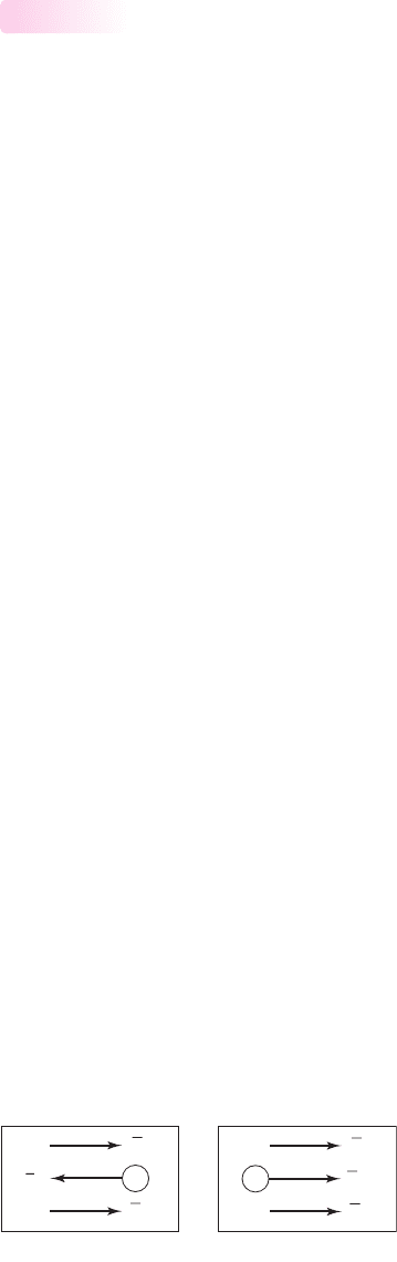
velocity and net movement. Consider an n-type semiconductor with a large number of
free electrons (Figure 1.8(a)). An electric field E applied in one direction produces a
force on the electrons in the opposite direction, because of the electrons’ negative
charge. The electrons acquire a drift velocity
v
dn
(in cm/s) which can be written as
v
dn
=−μ
n
E
(1.7)
where
μ
n
is a constant called the electron mobility and has units of cm
2
/V–s. For
low-doped silicon, the value of
μ
n
is typically 1350 cm
2
/V–s. The mobility can be
thought of as a parameter indicating how well an electron can move in a semicon-
ductor. The negative sign in Equation (1.7) indicates that the electron drift velocity is
opposite to that of the applied electric field as shown in Figure 1.8(a). The electron
drift produces a drift current density J
n
(A/cm
2
) given by
J
n
=−env
dn
=−en(−μ
n
E) =+enμ
n
E
(1.8)
where n is the electron concentration (#/cm
3
) and e, in this context, is the magnitude
of the electronic charge. The conventional drift current is in the opposite direction
from the flow of negative charge, which means that the drift current in an n-type
semiconductor is in the same direction as the applied electric field.
Next consider a p-type semiconductor with a large number of holes (Figure l.8(b)).
An electric field E applied in one direction produces a force on the holes in the same
direction, because of the positive charge on the holes. The holes acquire a drift
velocity
v
dp
(in cm/s), which can be written as
v
dp
=+μ
p
E
(1.9)
1.1.3
e
–
v
dn
J
n
E
n-type
h
+
v
dp
J
p
E
p-type
(b)(a)
Figure 1.8 Directions of applied electric field and resulting carrier drift velocity and drift
current density in (a) an n-type semiconductor and (b) a p-type semiconductor
nea80644_ch01_07-066.qxd 06/08/2009 05:15 PM Page 17 F506 Tempwork:Dont' Del Rakesh:June:Rakesh 06-08-09:MHDQ134-01 Folder:MHDQ134-01: