Neamen D. Microelectronics: Circuit Analysis and Design
Подождите немного. Документ загружается.

28 Part 1 Semiconductor Devices and Basic Applications
Ideal Current–Voltage Relationship
As shown in Figure 1.16, an applied voltage results in a gradient in the minority car-
rier concentrations, which in turn causes diffusion currents. The theoretical relation-
ship between the voltage and the current in the pn junction is given by
i
D
= I
S
e
v
D
nV
T
−1
(1.18)
The parameter I
S
is the reverse-bias saturation current. For silicon pn junctions,
typical values of I
S
are in the range of
10
−18
to
10
−12
A. The actual value depends on the
doping concentrations and is also proportional to the cross-sectional area of the junc-
tion. The parameter V
T
is the thermal voltage, as defined in Equation (1.16), and is ap-
proximately V
T
= 0.026 V at room temperature. The parameter n is usually called the
emission coefficient or ideality factor, and its value is in the range
1 ≤ n ≤ 2
.
The emission coefficient n takes into account any recombination of electrons
and holes in the space-charge region. At very low current levels, recombination may
be a significant factor and the value of n may be close to 2. At higher current levels,
recombination is less a factor, and the value of n will be 1. Unless otherwise stated,
we will assume the emission coefficient is
n = 1
.
This pn junction, with nonlinear rectifying current characteristics, is called a pn
junction diode.
EXAMPLE 1.7
Objective: Determine the current in a pn junction diode.
Consider a pn junction at
T = 300
K in which
I
S
= 10
−14
A
and
n = 1
. Find the
diode current for
v
D
=+0.70
V and
v
D
=−0.70
V.
Solution: For
v
D
=+0.70
V, the pn junction is forward-biased and we find
i
D
= I
S
e
v
D
V
T
−1
= (10
−14
)
e
(
+0.70
0.026
)
−1
⇒ 4.93 mA
For
v
D
=−0.70 V
, the pn junction is reverse-biased and we find
i
D
= I
S
e
v
D
V
T
−1
= (10
−14
)
e
(
−0.70
0.026
)
−1
∼
=
−10
−14
A
1.2.4
Excess electron
concentration
Excess hole
concentration
Holes
Electrons
p
n
(x = 0)
p
n
(x)
p
x' x
x = 0 x' = 0
n
n
p
(x' = 0)
n
p
(x')
n
po
p
no
Figure 1.16 Steady-state minority carrier concentrations in a pn junction under forward bias.
The gradients in the minority carrier concentrations generate diffusion currents in the device.
nea80644_ch01_07-066.qxd 06/08/2009 05:15 PM Page 28 F506 Tempwork:Dont' Del Rakesh:June:Rakesh 06-08-09:MHDQ134-01 Folder:MHDQ134-01:
Chapter 1 Semiconductor Materials and Diodes 29
Forward-bias
region
Reverse-bias
region
i
D
(mA)
v
D
(V)
i
D
=
– I
S
1
2
3
4
5
–1.0 1.0
0
Figure 1.17 Ideal I–V characteristics of a pn junction diode for
I
S
= 10
−14
A
. The diode
current is an exponential function of diode voltage in the forward-bias region and is very
nearly zero in the reverse-bias region. The pn junction diode is a nonlinear electronic device.
Comment:
Although I
S
is quite small, even a relatively small value of forward-bias
voltage can induce a moderate junction current. With a reverse-bias voltage applied,
the junction current is virtually zero.
EXERCISE PROBLEM
Ex 1.7: (a) A silicon pn junction at
T = 300
K has a reverse-saturation current of
I
S
= 2 ×10
−14
A
. Determine the required forward-bias voltage to produce a
current of (i)
I
D
= 50 μA
and (ii)
I
D
= 1mA
. (b) Repeat part (a) for
I
S
= 2 ×10
−12
A
. (Ans. (a) (i) 0.563 V, (ii) 0.641 V; (b) (i) 0.443 V, (ii) 0.521 V).
pn Junction Diode
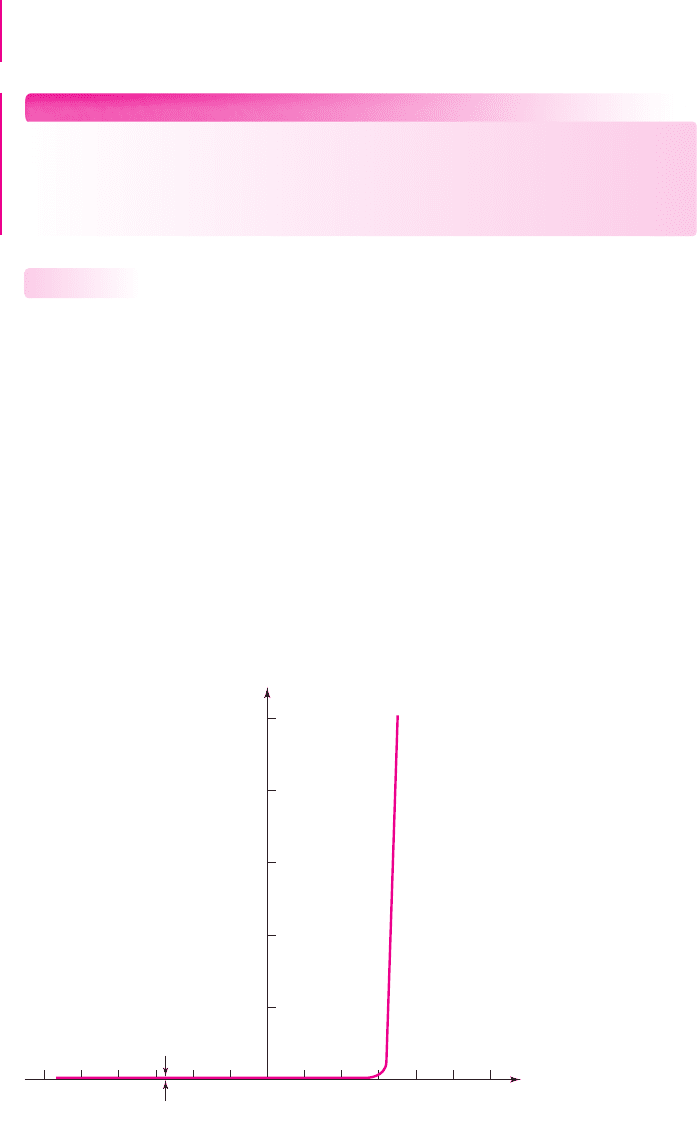
Figure 1.17 is a plot of the derived current–voltage characteristics of a pn junction.
For a forward-bias voltage, the current is an exponential function of voltage. Fig-
ure 1.18 depicts the forward-bias current plotted on a log scale. With only a small
change in the forward-bias voltage, the corresponding forward-bias current increases
by orders of magnitude. For a forward-bias voltage
v
D
> +0.1V
, the
(−1)
term in
Equation (1.18) can be neglected. In the reverse-bias direction, the current is al-
most zero.
Figure 1.19 shows the diode circuit symbol and the conventional current direc-
tion and voltage polarity. The diode can be thought of and used as a voltage con-
trolled switch that is “off” for a reverse-bias voltage and “on” for a forward-bias
voltage. In the forward-bias or “on” state, a relatively large current is produced by a
fairly small applied voltage; in the reverse-bias, or “off” state, only a very small cur-
rent is created.
1.2.5
nea80644_ch01_07-066.qxd 06/08/2009 05:15 PM Page 29 F506 Tempwork:Dont' Del Rakesh:June:Rakesh 06-08-09:MHDQ134-01 Folder:MHDQ134-01:

30 Part 1 Semiconductor Devices and Basic Applications
When a diode is reverse-biased by at least 0.1 V, the diode current is
i
D
=−I
S
. The
current is in the reverse direction and is a constant, hence the name reverse-bias satura-
tion current. Real diodes, however, exhibit reverse-bias currents that are considerably
larger than I
S
. This additional current is called a generation current and is due to electrons
and holes being generated within the space-charge region. Whereas a typical value of I
S
may be
10
−14
A
, a typical value of reverse-bias current may be
10
−9
A
or 1 nA. Even
though this current is much larger than I
S
, it is still small and negligible in most cases.
Temperature Effects
Since both I
S
and V
T
are functions of temperature, the diode characteristics also vary with
temperature. The temperature-related variations in forward-bias characteristics are illus-
trated in Figure 1.20. For a given current, the required forward-bias voltage decreases as
temperature increases. For silicon diodes, the change is approximately 2 mV/°C.
The parameter I
S
is a function of the intrinsic carrier concentration n
i
, which in
turn is strongly dependent on temperature. Consequently, the value of I
S
approxi-
mately doubles for every 5 °C increase in temperature. The actual reverse-bias diode
current, as a general rule, doubles for every 10 °C rise in temperature. As an example
of the importance of this effect, the relative value of n
i
in germanium, is large,
resulting in a large reverse-saturation current in germanium-based diodes. Increases
in this reverse current with increases in the temperature make the germanium diode
highly impractical for most circuit applications.
Breakdown Voltage
When a reverse-bias voltage is applied to a pn junction, the electric field in the space-
charge region increases. The electric field may become large enough that covalent
0
10
–14
i
D
(A)
v
D
(V)
I
S
0.1 0.2 0.3 0.4 0.5 0.6 0.7
10
–13
10
–12
10
–11
10
–10
10
–9
10
–8
10
–7
10
–6
10
–5
10
–4
10
–3
Figure 1.18 Ideal forward-biased I–V characteristics of a pn junction diode, with the current
plotted an a log scale for
I
S
= 10
−14
A
and
n = 1
. The diode current increases
approximately one order of magnitude for every 60-mV increase in diode voltage.
i
D
+
–
v
D
(b)
(a)
n
p
+
–
v
D
i
D
Figure 1.19 The basic pn
junction diode: (a) simplified
geometry and (b) circuit
symbol, and conventional
current direction and voltage
polarity
nea80644_ch01_07-066.qxd 06/08/2009 05:15 PM Page 30 F506 Tempwork:Dont' Del Rakesh:June:Rakesh 06-08-09:MHDQ134-01 Folder:MHDQ134-01:
Chapter 1 Semiconductor Materials and Diodes 31
v
D
i
D
BV
2
BV
1
Low
doped
High
doped
Figure 1.21 Reverse-biased diode characteristics
showing breakdown for a low-doped pn junction and
a high-doped pn junction. The reverse-bias current
increases rapidly once breakdown has occurred.
bonds are broken and electron–hole pairs are created. Electrons are swept into the
n-region and holes are swept into the p-region by the electric field, generating a large
reverse bias current. This phenomenon is called breakdown. The reverse-bias cur-
rent created by the breakdown mechanism is limited only by the external circuit. If
the current is not sufficiently limited, a large power can be dissipated in the junction
that may damage the device and cause burnout. The current–voltage characteristic of
a diode in breakdown is shown in Figure 1.21.
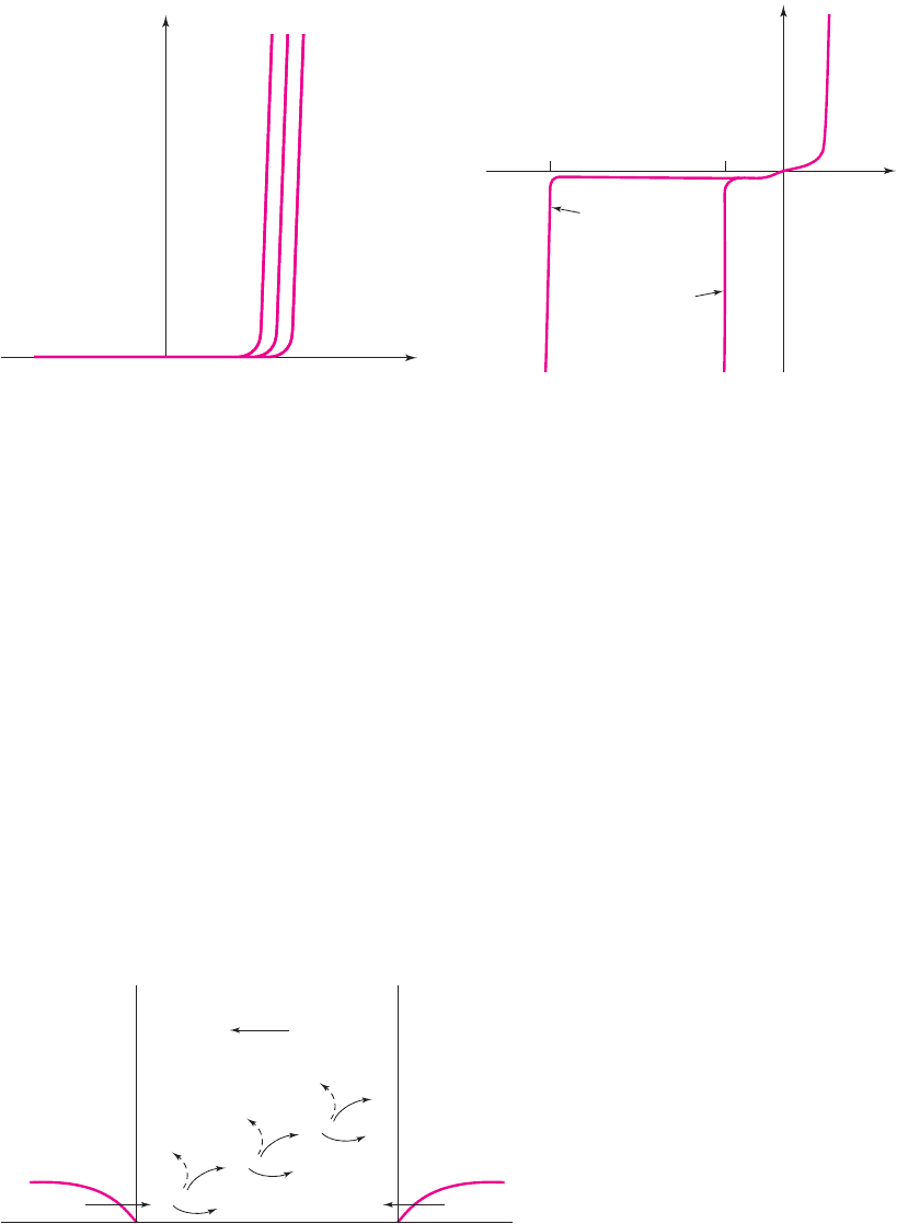
The most common breakdown mechanism is called avalanche breakdown,
which occurs when carriers crossing the space charge region gain sufficient kinetic
energy from the high electric field to be able to break covalent bonds during a
collision process. The basic avalanche multiplication process is demonstrated in
Figure 1.22. The generated electron–hole pairs can themselves be involved in a col-
lision process generating additional electron–hole pairs, thus the avalanche
process. The breakdown voltage is a function of the doping concentrations in the
i
D
T
2
T
1
T
0
v
D
0
T
2
> T
1
> T
0
Figure 1.20 Forward-biased pn junction
characteristics versus temperature. The required
diode voltage to produce a given current decreases
with an increase in temperature.
Figure 1.22 The avalanche multiplication process in the space charge region. Shown are the
collisions of electrons creating additional electron–hole pairs. Holes can also be involved in
collisions creating additional electron–hole pairs.
Diffusion
of holes
Diffusion of
electrons
Space charge region
⊗
⊗
(+)
(–)
(–)
(–)
p
n
pn
n
p
E – Field
(–)
(–)
(+)
⊗
(–)
(–)
(+)
nea80644_ch01_07-066.qxd 06/08/2009 05:15 PM Page 31 F506 Tempwork:Dont' Del Rakesh:June:Rakesh 06-08-09:MHDQ134-01 Folder:MHDQ134-01:
32 Part 1 Semiconductor Devices and Basic Applications
n- and p-regions of the junction. Larger doping concentrations result in smaller
breakdown voltages.
A second breakdown mechanism is called Zener breakdown and is a result of
tunneling of carriers across the junction. This effect is prominent at very high doping
concentrations and results in breakdown voltages less than 5 V.
The voltage at which breakdown occurs depends on fabrication parameters of the
pn junction, but is usually in the range of 50 to 200 V for discrete devices, although
breakdown voltages outside this range are possible—in excess of 1000 V, for example.
A pn junction is usually rated in terms of its peak inverse voltage or PIV. The PIV of a
diode must never be exceeded in circuit operation if reverse breakdown is to be avoided.
Diodes can be fabricated with a specifically designed breakdown voltage and are
designed to operate in the breakdown region. These diodes are called Zener diodes
and are discussed later in this chapter as well as in the next chapter.
Switching Transient
Since the pn junction diode can be used as an electrical switch, an important para-
meter is its transient response, that is, its speed and characteristics, as it is switched
from one state to the other. Assume, for example, that the diode is switched from the
forward-bias “on” state to the reverse-bias “off” state. Figure 1.23 shows a simple
circuit that will switch the applied voltage at time
t = 0
. For
t < 0
, the forward-bias
current i
D
is
i
D
= I
F
=
V
F
−v
D
R
F
(1.19)
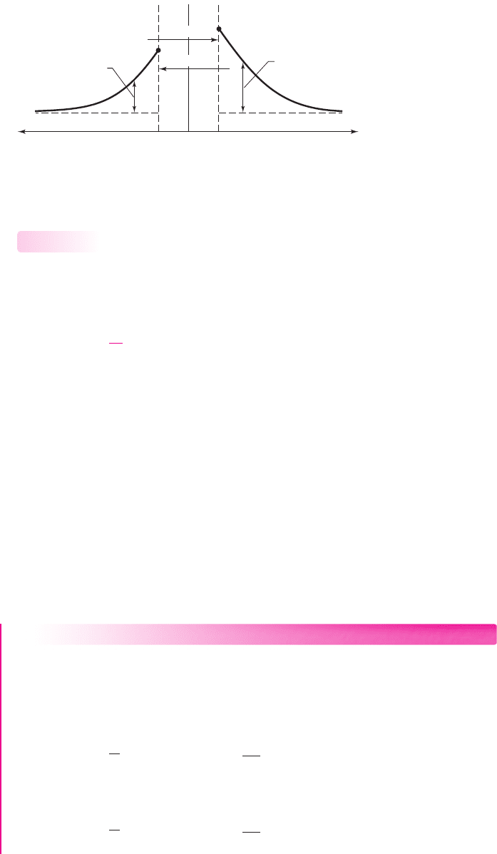
The minority carrier concentrations for an applied forward-bias voltage and an
applied reverse-bias voltage are shown in Figure 1.24. Here, we neglect the change
in the space charge region width. When a forward-bias voltage is applied, excess
minority carrier charge is stored in both the p- and n-regions. The excess charge is the
difference between the minority carrier concentrations for a forward-bias voltage and
those for a reverse-bias voltage as indicated in the figure. This charge must be
removed when the diode is switched from the forward to the reverse bias.
Excess minority
carrier electrons
Excess minority
carrier holes
Forward bias
Reverse bias
x' = 0 x = 0
pn
Minority carrier
concentrations
Figure 1.24 Stored excess minority carrier charge
under forward bias compared to reverse bias. This
charge must be removed as the diode is switched
from forward to reverse bias.
+
+
–
–
V
R
+
–
V
F
v
D
i
D
R
R
t = 0
R
F
I
F
I
R
n
p
Figure 1.23 Simple circuit for switching a
diode from forward to reverse bias
nea80644_ch01_07-066.qxd 06/08/2009 05:15 PM Page 32 F506 Tempwork:Dont' Del Rakesh:June:Rakesh 06-08-09:MHDQ134-01 Folder:MHDQ134-01:
Chapter 1 Semiconductor Materials and Diodes 33
i
D
I
F
–I
R
Time
0.1I
R
t
s
t
f
Figure 1.25 Current characteristics versus time during diode switching
As the forward-bias voltage is removed, relatively large diffusion currents are
created in the reverse-bias direction. This happens because the excess minority car-
rier electrons flow back across the junction into the n-region, and the excess minor-
ity carrier holes flow back across the junction into the p-region.
The large reverse-bias current is initially limited by resistor R
R
to approximately
i
D
=−I
R
∼
=
−V
R
R
R
(1.20)
The junction capacitances do not allow the junction voltage to change instanta-
neously. The reverse current I
R
is approximately constant for
0
+
< t < t
s
, where t
s
is
the storage time, which is the length of time required for the minority carrier con-
centrations at the space-charge region edges to reach the thermal equilibrium values.
After this time, the voltage across the junction begins to change. The fall time t
f
is
typically defined as the time required for the current to fall to 10 percent of its initial
value. The total turn-off time is the sum of the storage time and the fall time.
Figure 1.25 shows the current characteristics as this entire process takes place.
In order to switch a diode quickly, the diode must have a small excess minority
carrier lifetime, and we must be able to produce a large reverse current pulse.
Therefore, in the design of diode circuits, we must provide a path for the transient
reverse-bias current pulse. These same transient effects impact the switching of tran-
sistors. For example, the switching speed of transistors in digital circuits will affect
the speed of computers.
The turn-on transient occurs when the diode is switched from the “off” state to
the forward-bias “on” state, which can be initiated by applying a forward-bias current
pulse. The transient turn-on time is the time required to establish the forward-bias
minority carrier distributions. During this time, the voltage across the junction grad-
ually increases toward its steady-state value. Although the turn-on time for the pn
junction diode is not zero, it is usually less than the transient turn-off time.
Test Your Understanding
TYU 1.6 (a) Determine
V
bi
for a silicon pn junction at
T = 300
K for
N
a
=
10
15
cm
−3
and
N
d
= 5 ×10
16
cm
−3
. (b) Repeat part (a) for a GaAs pn junction.
(c) Repeat part (a) for a Ge pn junction. (Ans. (a) 0.679 V, (b) 1.15 V, (c) 0.296 V).
TYU 1.7 A silicon pn junction diode at
T = 300
K has a reverse-saturation current
of
I
S
= 10
−16
A
. (a) Determine the forward-bias diode current for (i)
V
D
= 0.55 V
,
nea80644_ch01_07-066.qxd 06/08/2009 05:15 PM Page 33 F506 Tempwork:Dont' Del Rakesh:June:Rakesh 06-08-09:MHDQ134-01 Folder:MHDQ134-01:

34 Part 1 Semiconductor Devices and Basic Applications
(ii)
V
D
= 0.65 V
, and (iii)
V
D
= 0.75 V
, (b) Find the reverse-bias diode current for
(i)
V
D
=−0.55 V
and (ii)
V
D
=−2.5V
. (Ans. (a) (i) 0.154
μ
A, (ii) 7.20
μ
A,
(iii) 0.337 mA; (b) (i)
−10
−16
A, (ii)
−10
−16
A).
TYU 1.8 Recall that the forward-bias diode voltage decreases approximately by
2 mV/
◦
C for silicon diodes with a given current. If
V
D
= 0.650 V
at
I
D
= 1mA
for
a temperature of 25
◦
C, determine the diode voltage at
I
D
= 1mA
for
T = 125
◦
C.
(Ans.
V
D
= 0.450 V
)
1.3 DIODE CIRCUITS: DC ANALYSIS AND MODELS
Objective: • Examine dc analysis techniques for diode circuits using
various models to describe the diode characteristics.
In this section, we begin to study the diode in various circuit configurations. As
we have seen, the diode is a two-terminal device with nonlinear i–v characteris-
tics, as opposed to a two-terminal resistor, which has a linear relationship between
current and voltage. The analysis of nonlinear electronic circuits is not as straight-
forward as the analysis of linear electric circuits. However, there are electronic
functions that can be implemented only by nonlinear circuits. Examples include
the generation of dc voltages from sinusoidal voltages and the implementation of
logic functions.
Mathematical relationships, or models, that describe the current–voltage
characteristics of electrical elements allow us to analyze and design circuits without
having to fabricate and test them in the laboratory. An example is Ohm’s law, which
describes the properties of a resistor. In this section, we will develop the dc analysis
and modeling techniques of diode circuits.
This section considers the current–voltage characteristics of the pn junction
diode in order to construct various circuit models. Large-signal models are initially
developed that describe the behavior of the device with relatively large changes in
voltages and currents. These models simplify the analysis of diode circuits and make
the analysis of relatively complex circuits much easier. In the next section, we will
consider a small-signal model of the diode that will describe the behavior of the pn
junction with small changes in voltages and currents. It is important to understand the
difference between large-signal and small-signal models and the conditions when
they are used.
To begin to understand diode circuits, consider a simple diode application. The
current–voltage characteristics of the pn junction diode were given in Figure 1.17.
An ideal diode (as opposed to a diode with ideal I–V characteristics) has the char-
acteristics shown in Figure 1.26(a). When a reverse-bias voltage is applied, the cur-
rent through the diode is zero (Figure 1.26(b)); when current through the diode is
greater than zero, the voltage across the diode is zero (Figure 1.26(c)). An external
circuit connected to the diode must be designed to control the forward current
through the diode.
One diode circuit is the rectifier circuit shown in Figure 1.27(a). Assume that
the input voltage
v
I
is a sinusoidal signal, as shown in Figure 1.27(b), and the diode
is an ideal diode (see Figure 1.26(a)). During the positive half-cycle of the sinusoidal
nea80644_ch01_07-066.qxd 06/08/2009 05:15 PM Page 34 F506 Tempwork:Dont' Del Rakesh:June:Rakesh 06-08-09:MHDQ134-01 Folder:MHDQ134-01:

Chapter 1 Semiconductor Materials and Diodes 35
+
+
–
–
v
O
v
D
v
I
R
+
–
i
D
v
I
02pp 3pwt
wt
+
–
v
R
v
I
v
I
> 0
+
–
i
D
+
–
v
O
= 0
R
v
I
+
–
i
D
= 0
v
I
< 0
02p
3p
v
O
(c)
(a)
(b)
(d) (e)
O
p
Figure 1.27 The diode rectifier: (a) circuit, (b) sinusoidal input signal, (c) equivalent circuit
for
v
I
> 0
, (d) equivalent circuit for
v
I
< 0
, and (e) rectified output signal
input, a forward-bias current exists in the diode and the voltage across the diode is
zero. The equivalent circuit for this condition is shown in Figure 1.27(c). The output
voltage
v
O
is then equal to the input voltage. During the negative half-cycle of the
sinusoidal input, the diode is reverse biased. The equivalent circuit for this condition
is shown in Figure 1.27(d). In this part of the cycle, the diode acts as an open circuit,
the current is zero, and the output voltage is zero. The output voltage of the circuit is
shown in Figure 1.27(e).
Over the entire cycle, the input signal is sinusoidal and has a zero average value;
however, the output signal contains only positive values and therefore has a positive
average value. Consequently, this circuit is said to rectify the input signal, which is
the first step in generating a dc voltage from a sinusoidal (ac) voltage. A dc voltage is
required in virtually all electronic circuits.
As mentioned, the analysis of nonlinear circuits is not as straightforward as that
of linear circuits. In this section, we will look at four approaches to the dc analysis of
diode circuits: (a) iteration; (b) graphical techniques; (c) a piecewise linear modeling
method; and (d) a computer analysis. Methods (a) and (b) are closely related and are
therefore presented together.
i
D
v
D
0
Reverse bias
Conducting
state
+–
v
D
(v
D
< 0, i
D
= 0)
i
D
= 0
+–
v
D
(i
D
> 0, v
D
= 0)
i
D
(a) (b) (c)
Figure 1.26 The ideal diode: (a) the I–V characteristics of the ideal diode, (b) equivalent
circuit under reverse bias (an open circuit), and (c) equivalent circuit in the conducting state
(a short circuit)
nea80644_ch01_07-066.qxd 06/08/2009 05:15 PM Page 35 F506 Tempwork:Dont' Del Rakesh:June:Rakesh 06-08-09:MHDQ134-01 Folder:MHDQ134-01:

36 Part 1 Semiconductor Devices and Basic Applications
Iteration and Graphical Analysis Techniques
Iteration means using trial and error to find a solution to a problem. The graphical
analysis technique involves plotting two simultaneous equations and locating their
point of intersection, which is the solution to the two equations. We will use both
techniques to solve the circuit equations, which include the diode equation. These
equations are difficult to solve by hand because they contain both linear and expo-
nential terms.
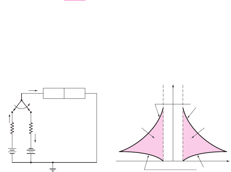
Consider, for example, the circuit shown in Figure 1.28, with a dc voltage V
PS
applied across a resistor and a diode. Kirchhoff’s voltage law applies both to non-
linear and linear circuits, so we can write
V
PS
= I
D
R + V
D
(1.21(a))
which can be rewritten as
I
D
=
V
PS
R
−
V
D
R
(1.21(b))
[Note: In the remainder of this section in which dc analysis is emphasized, the dc
variables are denoted by uppercase letters and uppercase subscripts.]
The diode voltage
V
D
and current
I
D
are related by the ideal diode equation as
I
D
= I
S
e
V
D
V
T
−1
(1.22)
where
I
S
is assumed to be known for a particular diode.
Combining Equations (1.21(a)) and (1.22), we obtain
V
PS
= I
S
R
e
V
D
V
T
−1
+ V
D
(1.23)
which contains only one unknown,
V
D
. However, Equation (1.23) is a transcendental
equation and cannot be solved directly. The use of iteration to find a solution to this
equation is demonstrated in the following example.
EXAMPLE 1.8
Objective: Determine the diode voltage and current for the circuit shown in
Figure 1.28.
Consider a diode with a given reverse-saturation current of
I
S
= 10
−13
A
.
Solution: We can write Equation (1.23) as
5 = (10
−13
)(2 × 10
3
)
e
V
D
0.026
−1
+ V
D
(1.24)
If we first try
V
D
= 0.60 V
, the right side of Equation (1.24) is 2.7 V, so the equa-
tion is not balanced and we must try again. If we next try
V
D
= 0.65 V
, the right
side of Equation (1.24) is 15.1 V. Again, the equation is not balanced, but we can
see that the solution for
V
D
is between 0.6 and 0.65 V. If we continue refining our
guesses, we will be able to show that, when
V
D
= 0.619 V
, the right side of Equa-
tion (1.29) is 4.99 V, which is essentially equal to the value of the left side of the
equation.
1.3.1
+
–
+
–
V
PS
= 5 V
I
D
V
D
R = 2 kΩ
Figure 1.28 A simple diode
circuit
nea80644_ch01_07-066.qxd 06/08/2009 05:15 PM Page 36 F506 Tempwork:Dont' Del Rakesh:June:Rakesh 06-08-09:MHDQ134-01 Folder:MHDQ134-01:

Chapter 1 Semiconductor Materials and Diodes 37
The current in the circuit can then be determined by dividing the voltage differ-
ence across the resistor by the resistance, or
I
D
=
V
PS
− V
D
R
=
5 − 0.619
2
= 2.19 mA
Comment: Once the diode voltage is known, the current can also be determined
from the ideal diode equation. However, dividing the voltage difference across a re-
sistor by the resistance is usually easier, and this approach is used extensively in the
analysis of diode and transistor circuits.
EXERCISE PROBLEM
Ex 1.8: Consider the circuit in Figure 1.28. Let
V
PS
= 4V
,
R = 4k
, and
I
S
= 10
−12
A
. Determine
V
D
and
I
D
, using the ideal diode equation and the itera-
tion method. (Ans.
V
D
= 0.535 V
,
I
D
= 0.866 mA
)
To use a graphical approach to analyze the circuit, we go back to Kirchhoff’s
voltage law, as expressed by Equation (1.21(a)), which was
V
PS
= I
D
R + V
D
. Solv-
ing for the current
I
D
, we have
I
D
=
V
PS
R
−
V
D
R
which was also given by Equation (1.21(b)). This equation gives a linear relation be-
tween the diode current
I
D
and the diode voltage
V
D
for a given power supply volt-
age
V
PS
and resistance R. This equation is referred to as the circuit load line, and is
usually plotted on a graph with the current
I
D
as the vertical axis and the voltage
V
D
as the horizontal axis.
From Equation (1.21(b)), we see that if
I
D
= 0
, then
V
D
= V
PS
which is the
horizontal axis intercept. Also from this equation, if
V
D
= 0
, then
I
D
= V
PS
/R
which is the vertical axis intercept. The load line can be drawn between these two
points. From Equation (1.21(b)), we see that the slope of the load line is
−1/R
.
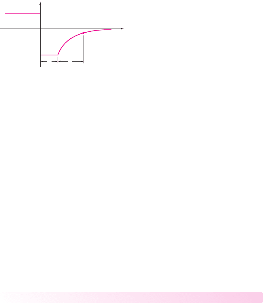
Using the values given in Example (1.8), we can plot the straight line shown in
Figure 1.29. The second plot in the figure is that of Equation (1.22), which is the ideal
diode equation relating the diode current and voltage. The intersection of the load
line and the device characteristics curve provides the dc current
I
D
≈ 2.2
mA
through the diode and the dc voltage
V
D
≈ 0.62 V
across the diode. This point is
referred to as the quiescent point, or the Q-point.
The graphical analysis method can yield accurate results, but it is somewhat
cumbersome. However, the concept of the load line and the graphical approach are
useful for “visualizing” the response of a circuit, and the load line is used extensively
in the evaluation of electronic circuits.
Piecewise Linear Model
Another, simpler way to analyze diode circuits is to approximate the diode’s
current–voltage characteristics, using linear relationships or straight lines. Figure 1.30,
for example, shows the ideal current–voltage characteristics and two linear
approximations.
1.3.2
nea80644_ch01_07-066.qxd 06/08/2009 05:15 PM Page 37 F506 Tempwork:Dont' Del Rakesh:June:Rakesh 06-08-09:MHDQ134-01 Folder:MHDQ134-01: