Neamen D. Microelectronics: Circuit Analysis and Design
Подождите немного. Документ загружается.

538 Part 1 Semiconductor Devices and Basic Applications
Solution (DC Analysis): We find, for each stage,
R
TH
= R
1
R
2
= 5531 = 19.83 k
and
V
TH
=
R
2
R
1
+ R
2
V
CC
=
31
31 + 55
(5) = 1.802 V
Now
I
BQ
=
V
TH
− V
BE
(on)
R
TH
+(1 +β)R
E
=
1.802 − 0.7
19.83 + (201)(1)
⇒ 4.99 μA
so that
I
CQ
= 0.998 mA
Solution (AC Analysis): The small-signal diffusion resistance is
r
π
=
βV
T
I
CQ
=
(200)(0.026)
0.988
= 5.21 k
The input resistance looking into each base terminal is
R
i
= r
π
+(1 +β)R
E
= 5.21 +(201)(1) = 206.2k
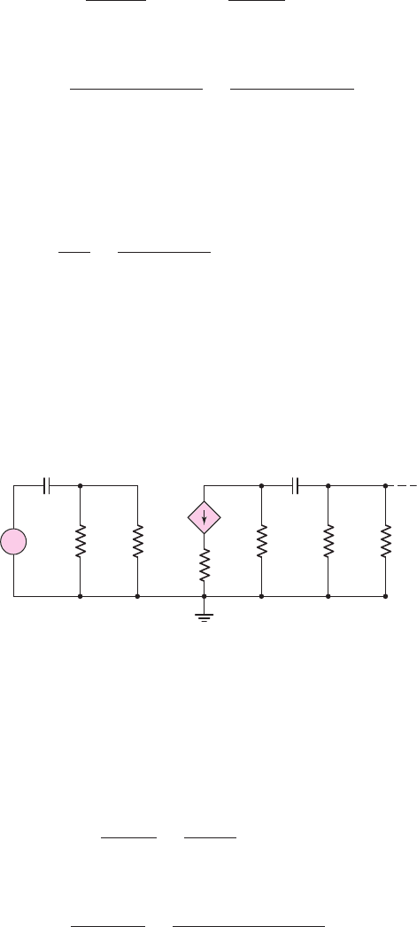
Solution (AC Design): The small-signal equivalent circuit is shown in Figure 7.74.
The time constant of the first stage is
τ
A
= (R
1
R
2
R
i
)C
C1
C
C1
C
C2
R
E1
R
C1
V
i
+
–
g
m
V
p
R
1
⎪⎪ R
2
R
1
⎪⎪ R
2
R
i
R
i
Figure 7.74 Small-signal equivalent circuit of two-stage BJT amplifier with coupling
capacitors for design application
and the time constant of the second stage is
τ
B
= (R
C1
+ R
1
R
2
R
i
)C
C2
If the 3 dB frequency of each stage is to be 20 Hz, then
τ
A
= τ
B
=
1
2π f
3-dB
=
1
2π(20)
= 7.958 ×10
−3
s
The coupling capacitor of the first stage must be
C
C1
=
τ
A
R
1
R
2
R
i
=
7.958 × 10
−3
(5531206.2) × 10
3
⇒ 0.44 μF
nea80644_ch07_469-558.qxd 06/13/2009 08:07 PM Page 538 F506 Hard disk:Desktop Folder:Rakesh:MHDQ134-07:

Chapter 7 Frequency Response 539
and the coupling capacitor of the second stage must be
C
C2
=
τ
B
R
C1
+ R
1
R
2
R
i
=
7.958 × 10
−3
(2.5 + 5531206.2) × 10
3
⇒ 0.386 μF
Comment: This circuit design using two coupling capacitors is a brute-force
approach to a two-stage amplifier design and would not be used in an IC design.
Since the 3 dB frequency for each capacitor is 20 Hz, this circuit is referred to as
a two-pole high-pass filter.
7.8 SUMMARY
• In this chapter, the frequency response of transistor circuits was discussed. The ef-
fects due to circuit capacitors, such as coupling, bypass, and load capacitors, were
determined. In addition, expanded equivalent circuits of BJTs and MOSFETs
were analyzed to determine the frequency response of the transistors.
• A time-constant technique was developed so that Bode plots can be constructed
without the need of deriving complex transfer functions. The high and low cor-
ner frequencies, or 3 dB frequencies, can be determined directly from the time
constants.
• Coupling and bypass capacitors affect the low-frequency characteristics of a cir-
cuit, while load capacitors affect the high-frequency characteristics of a circuit.
• The capacitances included in the small-signal equivalent circuits of both the
bipolar and MOS transistors result in reduced transistor gain at high frequencies.
The cutoff frequency is a figure of merit for the transistor and is defined as the
frequency at which the magnitude of the current gain is unity.
• The Miller effect is a multiplication of the base–collector or gate–drain capaci-
tance due to feedback between the output and input of the transistor. The band-
width of the amplifier is reduced by this affect.
• The common-emitter (common-source) amplifier, in general, shows the greatest
reduction in bandwidth due to the Miller effect. The common-base (common-
gate) amplifier has a larger bandwidth because of a smaller multiplication factor.
The cascode configuration, a combination of a common emitter and common
base, combines the advantages of high gain and wide bandwith.
• As an application, a two-stage BJT amplifier was designed to meet specified
3 dB frequencies.
CHECKPOINT
After studying this chapter, the reader should have the ability to:
✓ Construct the Bode plots of the gain magnitude and phase from a transfer func-
tion written in terms of the complex frequency s.
✓ Construct the Bode plots of the gain magnitude and phase of electronic amplifier
circuits, taking into account circuit capacitors, using the time constant technique.
✓ Determine the short-circuit current gain versus frequency of a BJT and deter-
mine the Miller capacitance of a BJT circuit using the expanded hybrid-π equiv-
alent circuit.
✓ Determine the unity-gain bandwidth of an FET and determine the Miller capac-
itance of an FET circuit using the expanded small-signal equivalent circuit.
✓ Describe the relative frequency responses of the three basic amplifier configura-
tions and the cascode amplifier.
nea80644_ch07_469-558.qxd 06/13/2009 08:07 PM Page 539 F506 Hard disk:Desktop Folder:Rakesh:MHDQ134-07:

540 Part 1 Semiconductor Devices and Basic Applications
REVIEW QUESTIONS
1. Describe the general frequency response of an amplifier and define the low-
frequency, midband, and high-frequency ranges.
2. Describe the general characteristics of the equivalent circuits that apply to the
low-frequency, midband, and high-frequency ranges.
3. Describe what is meant by a system transfer function in the s-domain.
4. What is the criterion that defines a corner, or 3 dB, frequency?
5. Describe what is meant by the phase of the transfer function.
6. Describe the time constant technique for determining the corner frequencies.
7. Describe the general frequency response of a coupling capacitor, a bypass
capacitor, and a load capacitor.
8. Sketch the expanded hybrid-
π
model of the BJT.
9. Describe the short-circuit current gain versus frequency response of a BJT and
define the cutoff frequency.
10. Describe the Miller effect and the Miller capacitance.
11. What effect does the Miller capacitance have on the amplifier bandwidth?
12. Sketch the expanded small-signal equivalent circuit of a MOSFET.
13. Define the cutoff frequency for a MOSFET.
14. What is the major contribution to the Miller capacitance in a MOSFET?
15. Why is there not a Miller effect in a common-base circuit?
16. Describe the configuration of a cascode amplifier.
17. Why is the bandwidth of a cascode amplifier larger, in general, than that of a
simple common-emitter amplifier?
18. Why is the bandwidth of the emitter-follower amplifier the largest of the three
basic BJT amplifiers?
PROBLEMS
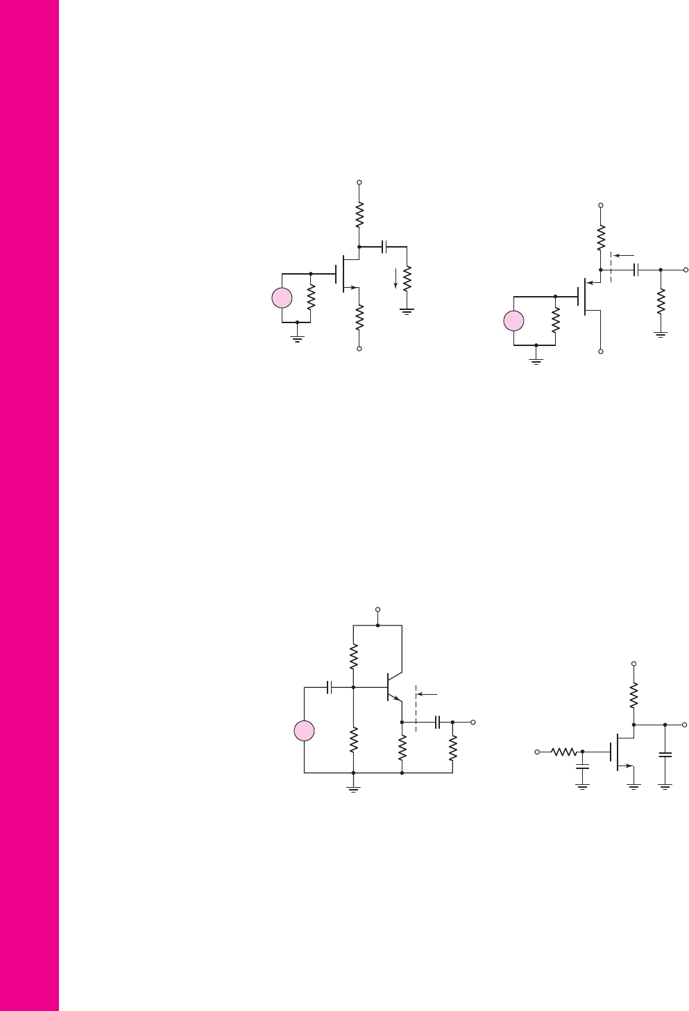
Section 7.2 System Transfer Functions
7.1 (a) Determine the voltage transfer function
T (s) = V
o
(s)/ V
i
(s)
for the cir-
cuit shown in Figure P7.1. (b) Sketch the Bode magnitude plot and deter-
mine the corner frequency. (c) Determine the time response of the circuit to
an input step function of magnitude
V
Io
.
V
o
V
i
R
1
= 1 kΩ
C
1
= 1
m
F
Figure P7.1
V
o
V
i
R
2
= 10 kΩ
C
2
= 10
m
F
Figure P7.2
7.2 Repeat Problem 7.1 for the circuit in Figure P7.2.
7.3 Consider the circuit in Figure P7.3. (a) Derive the expression for the voltage
transfer function
T(s) = V
o
(s)/V
i
(s)
. (b) What is the time constant associ-
ated with this circuit? (c) Find the corner frequency. (d) Sketch the Bode
magnitude plot of the voltage transfer function.
7.4 Consider the circuit in Figure P7.4 with a signal current source. The circuit
parameters are
R
i
= 30
k
,
R
P
= 10
k
,
C
S
= 10 μ
F, and
C
P
= 50
pF.
nea80644_ch07_469-558.qxd 06/13/2009 08:07 PM Page 540 F506 Hard disk:Desktop Folder:Rakesh:MHDQ134-07:
Chapter 7 Frequency Response 541
(a) Determine the open-circuit time constant associated with C
S
and the
short-circuit time constant associated with
C
P
. (b) Determine the corner
frequencies and the magnitude of the transfer function
T (s) = V
o
(s)/I
i
(s)
at midband. (c) Sketch the Bode magnitude plot.
7.5 Consider the circuit shown in Figure P7.5. (a) What is the value of the volt-
age transfer function
V
o
/V
i
at very low frequencies? (b) Determine the volt-
age transfer function at very high frequencies. (c) Derive the expression for
the voltage transfer function
T (s) = V
o
(s)/V
i
(s)
. Put the expression in the
form
T (s) = K(1 +sτ
A
)/(1 + sτ
B
)
. What are the values of
K, τ
A
, and
τ
B
?
v
o
v
i
R
1
= 10 kΩ
R
2
= 20 kΩ
C
1
= 10
m
F
Figure P7.5
v
o
v
i
R
2
= 20 kΩ
R
1
= 10 kΩ
C
2
= 10
m
F
Figure P7.3
R
P
C
P
C
S
I
i
V
o
R
i
Figure P7.4
*7.6 (a) Derive the voltage transfer function
T (s) = V
o
(s)/ V
i
(s)
for the circuit
shown in Figure 7.10, taking both capacitors into account. (b) Let
R
S
= R
P
= 10
k
,
C
S
= 1
μF, and
C
P
= 10
pF. Calculate the actual mag-
nitude of the transfer function at
f
L
= 1/[(2π)(R
S
+ R
P
)C
S
]
and at
f
H
= 1/[(2π)(R
S
R
P
)C
P
]
. How do these magnitudes compare to the
maximum magnitude of
R
P
/(R
S
+ R
P
)
? (c) Repeat part (b) for
R
S
=
R
P
= 10
k
and
C
S
= C
P
= 0.1 μ
F.
7.7 A voltage transfer function is given by
T ( f ) = 1/(1 + jf/ f
T
)
3
. (a) Show
that the actual response at
f = f
T
is approximately 9 dB below the maxi-
mum value. What is the phase angle at this frequency? (b) What is the slope
of the magnitude plot for
f f
T
? What is the phase angle in this fre-
quency range?
7.8 Sketch the Bode magnitude plots for the following functions:
(a)
T
1
(s) =
s
s + 100
(b)
T
2
(s) =
5
s/2000 +1
(c)
T
3
(s) =
200(s + 10)
(s + 1000)
nea80644_ch07_469-558.qxd 06/13/2009 08:08 PM Page 541 F506 Hard disk:Desktop Folder:Rakesh:MHDQ134-07:
542 Part 1 Semiconductor Devices and Basic Applications
7.9 (a) (i) Sketch the Bode magnitude plot for the function
T (s) =
10(s + 10)(s + 100)
(s + 1)(s + 1000)
(ii) What are the corner frequencies? (iii) Determine
|
T (ω)
|
for
ω → 0
.
(iv) Determine
|
T (ω)
|
for
ω →∞
.
(b) Repeat part (a) for the function
T (s) =
8s
2
(0.2s + 1)
2
7.10 (a) Determine the transfer function corresponding to the Bode plot of the
magnitude shown in Figure P7.10. (b) What is the actual gain at
(i)
ω = 50
rad/s, (ii)
ω = 150
rad/s, and (iii)
ω = 100
krad/s.
T ( jw)
10
2
5
5×10
4
w (rad/s)
Figure P7.10
v
i
C
v
o
R
3
R
2
R
1
+
–
+
–
Figure P7.12
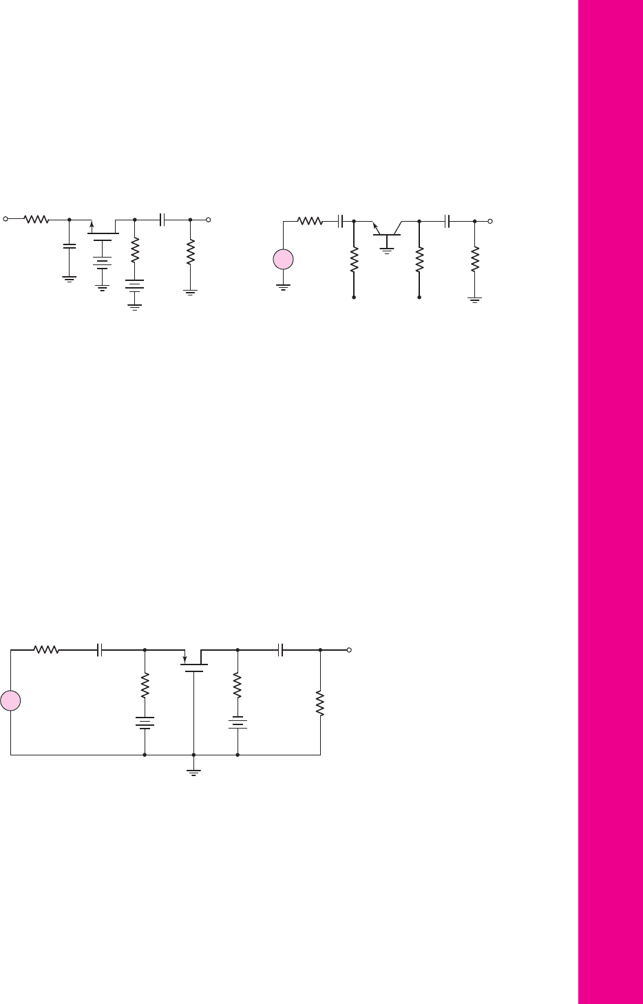
7.11 Consider the circuit shown in Figure 7.15 with parameters
R
S
= 0.5
k
,
r
π
= 5.2
k
,
g
m
= 29
mA/V, and
R
L
= 6
k
. The corner frequencies are
f
L
= 30
Hz and
f
H
= 480
kHz. (a) Calculate the midband voltage gain.
(b) What are the open-circuit and short-circuit time constants? (c) Deter-
mine
C
C
and
C
L
.
*7.12 For the circuit shown in Figure P7.12, the parameters are
R
1
= 10 k
,
R
2
= 10 k
,
R
3
= 40
k
, and
C = 10 μ
F. (a) What is the value of the volt-
age transfer function
V
o
/V
i
at very low frequencies? (b) Determine the
value of the voltage transfer function at very high frequencies. (c) Derive
the expression for the voltage transfer function
T (s) = V
o
(s)/V
i
(s)
. Put the
expression in the form
T (s) = K(1 +sτ
A
)/(1 + sτ
B
)
. What are the values
of
K, τ
A
, and
τ
B
?
7.13 The circuit shown in Figure 7.10 has parameters
R
S
= 1
k
,
R
P
= 10
k
,
and
C
S
= C
P
= 0.01 μ
F. Using PSpice, plot the magnitude and phase of
the voltage transfer function. Determine the maximum value of the voltage
transfer function. Determine the frequencies at which the magnitude is
1/
√
2
of the peak value.
Section 7.3 Frequency Response: Transistor Circuits
7.14 The transistor shown in Figure P7.14 has parameters
V
TN
= 0.4
V,
K
n
= 0.4 mA/V
2
, and
λ = 0
. The transistor is biased at
I
DQ
= 0.8
mA.
(a) What is the maximum voltage gain? (b) What is the bandwidth?
nea80644_ch07_469-558.qxd 06/13/2009 09:03 PM Page 542 F506 Hard disk:Desktop Folder:Rakesh:MHDQ134-07:
Chapter 7 Frequency Response 543
C
L
= 0.08 pF
V
o
V
i
R
C
V
CC
= 2.5 V
Figure P7.15
V
o
V
i
V
+
= 2.5 V
C
L
= 1 pF
R
D
=
1 kΩ
Figure P7.14
V
o
V
i
V
+
= 2.5 V
C
L
= 0.5 pF
I
DQ
=
100 mA
Figure P7.16
v
i
R
S
= 0.5 kΩ
C
C
= 0.1
m
F
V
CC
= 12 V
v
O
R
C
=
1 kΩ
R
E
=
0.1 kΩ
R
1
= 10 kΩ
R
2
= 1.5 kΩ
+
–
Figure P7.17
v
i
C
C
R
in
V
DD
= 9 V
v
O
R
D
R
S
=
0.5 kΩ
R
1
R
2
+
–
Figure P7.18
7.15 Consider the circuit shown in Figure P7.15. The transistor has parameters
β = 120
and
V
A
=∞
. The circuit bandwidth is 800 MHz and the quiescent
collector–emitter voltage is
V
CEQ
= 1.25
V. (a) Determine
R
C
, (b) find I
CQ
,
and (c) determine the maximum gain.
7.16 The transistor in the circuit shown in Figure P7.16 has parameters
V
TN
= 0.4
V,
K
n
= 50 μ
A/V
2
, and
λ = 0.01 V
−1
. (a) Derive the expression
for the voltage transfer function
T (s) = V
o
(s)/V
i
(s)
. (b) Determine the
maximum voltage gain. (c) What is the bandwidth?
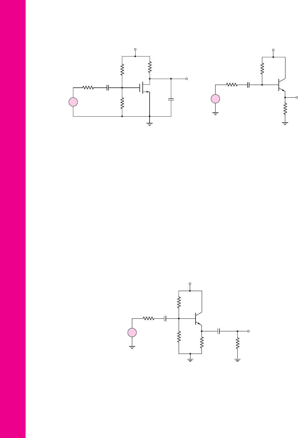
7.17 For the common-emitter circuit in Figure P7.17, the transistor parameters
are:
β = 100
,
V
BE
(on) = 0.7
V, and
V
A
=∞
. (a) Calculate the lower cor-
ner frequency. (b) Determine the midband voltage gain. (c) Sketch the Bode
plot of the voltage gain magnitude.
D7.18 (a) Design the circuit shown in Figure P7.18 such that
I
DQ
= 0.8
mA,
V
DSQ
= 3.2
V,
R
in
= 160
k
, and
f
L
= 16 Hz
. The transistor parameters are
K
n
= 0.5
mA/V
2
, V
TN
= 1.2
V, and
λ = 0
. (b) What is the midband volt-
age gain? (c) Determine the magnitude of the voltage gain at (i)
f = 5
Hz,
(ii)
f = 14
Hz, and (iii)
f = 25
Hz. (d) Sketch the Bode plot of the voltage
gain magnitude and phase.
D7.19 The transistor in the circuit in Figure P7.19 has parameters
K
n
=
0.5 mA/V
2
,
V
TN
= 1
V, and
λ = 0
. (a) Design the circuit such that
I
DQ
=
1 mA and
V
DSQ
= 3
V. (b) Derive the expression for the transfer function
nea80644_ch07_469-558.qxd 06/13/2009 08:08 PM Page 543 F506 Hard disk:Desktop Folder:Rakesh:MHDQ134-07:
544 Part 1 Semiconductor Devices and Basic Applications
T (s) = I
o
(s)/ V
i
(s)
. What is the expression for the circuit time constant?
(c) Determine C
C
such that the lower 3 dB frequency is 10 Hz. (d) Verify the
results of parts (a) and (c) with a computer simulation.
C
C
R
o
v
o
R
G
=
50 kΩ
R
S
= 12 kΩ
+9 V
–9 V
v
i
R
L
=
10 kΩ
+
–
Figure P7.20
v
o
v
i
C
C1
→ ∞
C
C2
= 2
m
F
R
o
V
CC
= 12 V
R
L
=
4 kΩ
R
1
R
2
R
E
=
4 kΩ
+
–
Figure P7.21
*D7.20 The transistor in the circuit in Figure P7.20 has parameters
K
p
=
0.5 mA/V
2
,
V
TP
=−2
V, and
λ = 0
. (a) Determine
R
o
. (b) What is the ex-
pression for the circuit time constant? (c) Determine
C
C
such that the
lower 3 dB frequency is 20 Hz.
7.21 For the circuit in Figure P7.21, the transistor parameters are
β = 120
,
V
BE
(on) = 0.7
V, and
V
A
= 50
V. (a) Design a bias-stable circuit such that
I
EQ
= 1.5
mA. (b) Using the results of part (a), find the small-signal mid-
band voltage gain. (c) Determine the output resistance
R
o
. (d) What is the
lower 3 dB corner frequency?
V
o
V
i
C
L
R
D
R
Si
C
i
V
DD
Figure P7.22
7.22 (a) For the circuit shown in Figure P7.22, write the voltage transfer function
T (s) = V
o
(s)/V
i
(s)
. Assume
λ>0
for the transistor. (b) What is the ex-
pression for the time constant associated with the input portion of the cir-
cuit? (c) What is the expression for the time constant associated with the
output portion of the circuit?
Figure P7.19
C
C
R
G
=
100 kΩ
R
S
R
D
+5 V
–5 V
v
i
R
L
= 4 kΩ
i
o
+
–
nea80644_ch07_469-558.qxd 06/13/2009 08:08 PM Page 544 F506 Hard disk:Desktop Folder:Rakesh:MHDQ134-07:
Chapter 7 Frequency Response 545
7.23 Consider the circuit shown in Figure P7.23. (a) Write the transfer function
T (s) = V
o
(s)/V
i
(s)
. Assume
λ = 0
for the transistor. (b) Determine the ex-
pression for the time constant associated with the input portion of the cir-
cuit. (c) Determine the expression for the time constant associated with the
output portion of the circuit.
v
I
v
O
C
C1
= 4.7
m
F
C
C 2
= 1
m
F
R
S
= 200 Ω
R
C
=
2 kΩ
R
L
=
47 kΩ
R
E
=
4 kΩ
V
–
= –5 V V
+
= 5 V
+
–
Figure P7.24
+
–
v
i
v
o
C
C1
= 4.7
m
F
C
C2
= 1
m
F
R
S
= 200 Ω
R
D
= 1.2 kΩ
R
L
= 50 kΩ
R
1
= 1.2 kΩ
+
5 V
–
–
5 V
+
Figure P7.26
*D7.27 A MOSFET amplifier with the configuration in Figure P7.27 is to be
designed for use in a telephone circuit. The magnitude of the voltage gain
should be 10 in the midband range, and the midband frequency range should
extend from 200 Hz to 3 kHz. [Note: A telephone’s frequency range does
not correspond to a high-fidelity system’s.] All resistor, capacitor, and
MOSFET parameters should be specified.
V
i
V
o
C
C
R
S
C
i
R
D
V
DD
R
L
+
–
V
G
+
–
Figure P7.23
7.24 The parameters of the transistor in the circuit in Figure P7.24 are
V
BE
(on) = 0.7
V,
β = 100
, and
V
A
=∞
. (a) Determine the quiescent and
small-signal parameters of the transistor. (b) Find the time constants asso-
ciated with
C
C1
and
C
C2
. (c) Is there a dominant
−3
dB frequency?
Estimate the
−3
dB frequency.
7.25 A capacitor is placed in parallel with R
L
in the circuit in Figure P7.24. The
capacitance is
C
L
= 10
pF. The transistor parameters are the same as given
in Problem 7.24. (a) Determine the upper −3 dB frequency. (b) Find the
high frequency value at which the small-signal voltage gain magnitude is
one-tenth the midband value.
7.26 The parameters of the transistor in the circuit in Figure P7.26 are
K
p
=
1 mA/V
2
,
V
TP
=−1.5
V, and
λ = 0
. (a) Determine the quiescent and
small-signal parameters of the transistor. (b) Find the time constants associ-
ated with
C
C1
and
C
C2
. (c) Is there a dominant pole frequency? Estimate the
−3
dB frequency.
nea80644_ch07_469-558.qxd 06/13/2009 08:08 PM Page 545 F506 Hard disk:Desktop Folder:Rakesh:MHDQ134-07:
546 Part 1 Semiconductor Devices and Basic Applications
7.28 The circuit in Figure P7.28 is a simple output stage of an audio amplifier.
The transistor parameters are
β = 200
,
V
BE
(on) = 0.7
V, and
V
A
=∞
. De-
termine
C
C
such that the lower
−3
dB frequency is 15 Hz.
7.29 Reconsider the circuit in Figure P7.28. The transistor parameters are
β = 120
,
V
BE
(on) = 0.7V
, and
V
A
=∞
. The circuit parameters are
V
+
=
3.3
V and
R
S
= 100
. (a) Find
R
B
and
R
E
such that
I
EQ
= 0.25
mA and
V
CEQ
= 1.8
V. (b) Using the results of part (a), find the value of
C
C
such
that
f
L
= 20
Hz. (c) Determine the midband voltage gain.
D7.30 The parameters of the transistor in the circuit in Figure P7.30 are
β = 100
,
V
BE
(on) = 0.7
V, and
V
A
=∞
. The time constant associated with
C
C1
is a
factor of 100 larger than the time constant associated with
C
C2
. (a) Deter-
mine
C
C2
such that the
−3
dB frequency associated with this capacitor is
25 Hz. (b) Determine
C
C1
.
D7.31 Consider the circuit shown in Figure P7.30. The time constant associated
with
C
C2
is a factor of 100 larger than the time constant associated with
C
C1
. (a) Determine
C
C1
such that the
−3
dB frequency associated with this
capacitor is 20 Hz. (b) Find
C
C2
.
+
–
v
s
v
o
V
+
= 10 V
C
C
R
S
= 500 Ω
R
B
= 430 kΩ
R
E
= 2.5 kΩ
Figure P7.28
+
–
v
i
v
o
V
DD
= 9 V
R
D
R
1
R
2
C
C
C
L
R
Si
= 200 Ω
Figure P7.27
+
–
v
s
v
o
V
CC
= 5 V
C
C1
C
C2
R
S
= 300 Ω
R
2
= 1.2 kΩ
R
E
= 50 Ω
R
L
= 10 Ω
R
1
= 1.2 kΩ
Figure P7.30
7.32 Consider the circuit shown in Figure P7.32. The transistor parameters are
β = 120
,
V
BE
(on) = 0.7V
, and
V
A
=∞
. (a) Find
R
C
such that
V
CEQ
= 2.2
V. (b) Determine the midband gain. (c) Derive the expression
for the corner frequencies associated with
C
C
and
C
E
. (d) Determine
C
C
nea80644_ch07_469-558.qxd 06/13/2009 08:08 PM Page 546 F506 Hard disk:Desktop Folder:Rakesh:MHDQ134-07:
Chapter 7 Frequency Response 547
and
C
E
such that the corner frequency associated with
C
E
is
f
E
= 10
Hz
and the corner frequency associated with
C
C
is
f
C
= 50
Hz.
+5 V
–5 V
R
D
R
S
v
i
v
O
C
S
= 5
m
F
+
–
Figure P7.33
v
i
R
C
R
L
= 20 kΩ
R
i
=
10 kΩ
I
Q
=
0.2 mA
C
C
C
E
+
–
v
o
V
+
= 3 V
V
−
= −3 V
Figure P7.32
*D7.33 For the transistor in the circuit in Figure P7.33, the parameters are:
K
n
= 0.5
mA/V
2
,
V
TN
= 0.8
V, and
λ = 0
. (a) Design the circuit such that
I
DQ
= 0.5
mA and
V
DSQ
= 4
V. (b) Determine the 3 dB frequencies. (c) If
the
R
S
resistor is replaced by a constant-current source producing the same
I
DQ
quiescent current, determine the 3 dB corner frequencies.
7.34 Figure P7.34 shows the ac equivalent circuit of two identical common-
source circuits in cascade. The transistor parameters are
K
n1
= K
n2
=
0.8
mA/V
2
,
λ
1
= λ
2
= 0.02
V
−1
, and
I
DQ1
= I
DQ2
= 0.5
mA. The circuit
parameters are
R
D
= 5k
and
C
L
= 12
pF. (a) Derive the expressions for
the voltage transfer functions (i)
T
1
(s) = V
o1
(s)/V
i
(s)
, (ii)
T
2
(s) =
V
o
(s)/V
o1
(s)
, and (iii)
T(s) = V
o
(s)/V
i
(s)
. (b) Determine the –3 dB fre-
quencies for (i)
T
1
(s)
, (ii)
T
2
(s)
, and (iii)
T(s)
. (c) Sketch the Bode plot for
the magnitude of the transfer function
T(s)
.
V
o
V
o1
R
D
R
D
V
i
C
L
C
L
M
2
M
1
Figure P7.34
V
+
V
–
R
E
C
E
R
C
v
i
v
O
+
–
Figure P7.35
*7.35 The common-emitter circuit in Figure P7.35 has an emitter bypass ca-
pacitor. (a) Derive the expression for the small-signal voltage gain
A
v
(s) = V
o
(s)/ V
i
(s)
. Write the expression in a form similar to that of
Equation (7.60). (b) What are the expressions for the time constants
τ
A
and τ
B
?
nea80644_ch07_469-558.qxd 06/13/2009 09:03 PM Page 547 F506 Hard disk:Desktop Folder:Rakesh:MHDQ134-07: