Neamen D. Microelectronics: Circuit Analysis and Design
Подождите немного. Документ загружается.

508 Part 1 Semiconductor Devices and Basic Applications
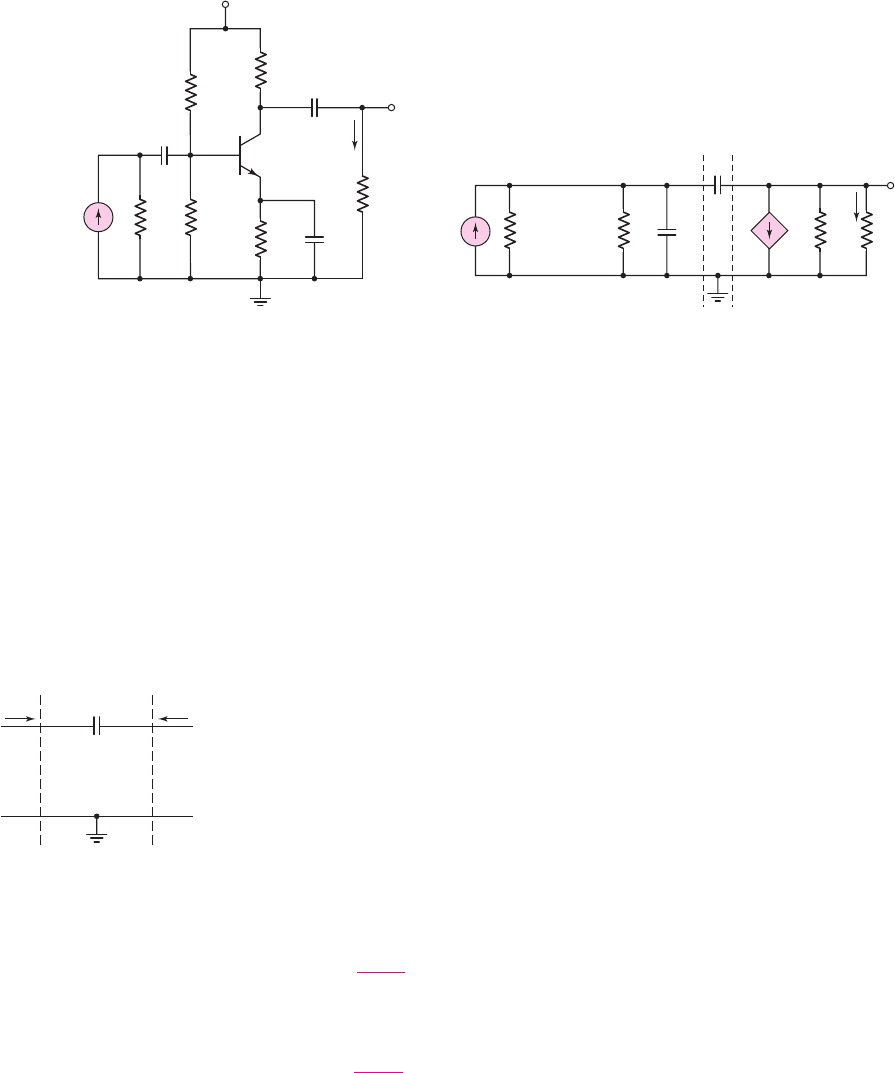
Figure 7.41(a) is a common-emitter circuit with a signal current source at
the input. We will determine the small-signal current gain
A
i
= i
o
/i
s
of the circuit.
Figure 7.41(b) is the small-signal equivalent circuit, assuming the frequency is
sufficiently high for the coupling and bypass capacitors to act as short circuits.
The transistor model is the simplified hybrid-
π
circuit shown in Figure 7.38
(assuming
r
o
=∞
). Capacitor C
μ
is a feedback element that connects the output
back to the input. The output voltage and current will therefore influence the input
characteristics.
The presence of
C
μ
complicates the analysis. Previously, we could write KCL
equations at the input and output nodes and derive an expression for the current gain.
Here, however, we will approach the problem differently. We will treat capacitor
C
μ
as a two-port network and will develop an equivalent circuit, with elements between
the input base and ground and between the output collector and ground. This proce-
dure may appear more complicated, but it will demonstrate the effect of
C
μ
more
clearly.
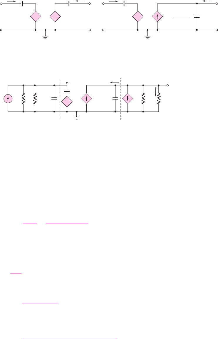
Consider the circuit segment between the two dotted lines in Figure 7.41(b). We
can treat this section as a two-port network, as shown in Figure 7.42. The input volt-
age is
V
π
and the output voltage is V
o
. Also, the input and output currents, I
1
and I
2
,
are defined as shown in the figure.
Writing KVL equations at the input and output terminals, we now have
V
π
= I
1
1
jωC
μ
+ V
o
(7.75(a))
and
V
o
= I
2
1
jωC
μ
+ V
π
(7.75(b))
Using Equations (7.75(a)) and (7.75(b)), we can form a two-port equivalent circuit,
as shown in Figure 7.43(a). We then convert the Thevenin equivalent circuit on the
output to a Norton equivalent circuit, as shown in Figure 7.43(b).
(a)
(b)
i
s
r
s
C
C1
C
E
v
o
R
C
V
CC
R
1
R
2
R
E
C
C2
R
L
i
o
r
p
g
m
V
p
C
m
R
C
V
o
R
L
R
B
=
r
s
⎪⎪ R
1
⎪⎪ R
2
C
p
I
s
I
o
+
–
V
p
Figure 7.41 (a) Common-emitter circuit with current source input; (b) small-signal
equivalent circuit with simplified hybrid-
π
model
C
m
+
–
V
p
+
–
V
o
I
2
I
1
Figure 7.42 Two-terminal
network of capacitor
C
μ
nea80644_ch07_469-558.qxd 06/13/2009 08:07 PM Page 508 F506 Hard disk:Desktop Folder:Rakesh:MHDQ134-07:
Chapter 7 Frequency Response 509
(a)
+
–
V
o
+
–
V
p
V
p
V
o
I
1
I
2
+
–
+
–
C
m
C
m
(b)
+
–
V
o
+
–
V
p
V
o
I
1
I
2
+
–
C
m
C
m
V
p
(1/ jwC
m
)
I
sc
=
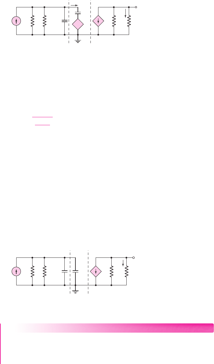
Figure 7.43 (a) Two-port equivalent circuit of capacitor
C
μ
with equivalent output circuits:
(a) Thevenin equivalent and (b) Norton equivalent
C
p
C
m
V
o
I
s
V
o
R
B
+
–
V
p
r
p
R
L
R
C
C
m
+
–
I
o
g
m
V
p
I
sc
=
jwC
m
V
p
I
1
I
2
Figure 7.44 Small-signal equivalent circuit, including the two-port equivalent model of
capictor
C
μ
The equivalent circuit in Figure 7.43(b) replaces the circuit segment between the
dotted lines in Figure 7.41(b), and the modified circuit is shown in Figure 7.44. To
evaluate this circuit, we will make some simplifying approximations.
Typical values of g
m
and
C
μ
are
g
m
= 50 mA/V
and
C
μ
= 0.05
pF. From these
values, we can calculate the frequency at which the magnitudes of the two dependent
current sources are equal. If
ωC
μ
V
π
= g
m
V
π
(7.76(a))
then
f =
g
m
2πC
μ
=
50 × 10
−3
2π(0.05 ×10
−12
)
= 1.59 ×10
11
Hz
⇒ 159 GHz
(7.76(b))
Since the frequency of operation of bipolar transistors is far less than 159 GHz, the
current source
I
sc
= jωC
μ
V
π
is negligible compared to the
g
m
V
π
source.
We can now calculate the frequency at which the magnitude of the impedance of
C
μ
is equal to
R
C
R
L
. If
1
ωC
μ
= R
C
R
L
(7.77(a))
then
f =
1
2πC
μ
(R
C
R
L
)
(7.77(b))
If we assume
R
C
= R
L
= 4k
, which are typical values for discrete bipolar
circuits, then
f =
1
2π(0.05 ×10
−12
)[(4 × 10
3
)(4 × 10
3
)]
= 1.59 ×10
9
Hz
(7.78)
nea80644_ch07_469-558.qxd 06/13/2009 08:07 PM Page 509 F506 Hard disk:Desktop Folder:Rakesh:MHDQ134-07:
r
p
C
p
g
m
V
p
R
L
C
m
V
o
R
C
I
s
V
o
I
o
I
1
R
B
+
–
V
p
+
–
Figure 7.45 Small-signal equivalent circuit, including approximations
r
p
C
p
g
m
V
p
R
L
C
M
R
C
I
s
V
o
I
o
R
B
+
–
V
p
Figure 7.46 Small-signal equivalent circuit, including the equivalent Miller capacitance
510
Part 1 Semiconductor Devices and Basic Applications
If the frequency of operation of the bipolar transistor is very much smaller than
1.59 GHz, then the impedance of
C
μ
will be much greater than
R
C
R
L
and
C
μ
can
be considered an open circuit. Using these approximations, the circuit in Figure 7.44
reduces to that shown in Figure 7.45.
The I
1
versus V
π
characteristic of the circuit segment between the dotted lines is
I
1
=
V
π
− V
o
1
jωC
μ
= jωC
μ
(V
π
− V
o
)
(7.79)
The output voltage is
V
o
=−g
m
V
π
(R
C
R
L
)
(7.80)
Substituting Equation (7.80) into (7.79), we obtain
I
1
= jωC
μ
[1 + g
m
(R
C
R
L
)]V
π
(7.81)
In Figure 7.45, the circuit segment between the dotted lines can be replaced by
an equivalent capacitance given by
C
M
= C
μ
[1 + g
m
(R
C
R
L
)]
(7.82)
as shown in Figure 7.46. Capacitance C
M
is called the Miller capacitance, and the
multiplication effect of C
µ
is the Miller effect.
For the equivalent circuit in Figure 7.46, the input capacitance is now
C
π
+C
M
,
rather than just
C
π
if
C
μ
had been ignored.
EXAMPLE 7.10
Objective: Determine the 3 dB frequency of the current gain for the circuit shown in
Figure 7.46, both with and without the effect of C
M
.
The circuit parameters are:
R
C
= R
L
= 4k
,
r
π
= 2.6k
,
R
B
= 200 k
,
C
π
= 0.8pF
,
C
μ
= 0.05 pF
, and
g
m
= 38.5mA/V
.
nea80644_ch07_469-558.qxd 06/13/2009 08:07 PM Page 510 F506 Hard disk:Desktop Folder:Rakesh:MHDQ134-07:

Chapter 7 Frequency Response 511
Solution: The output current can be written as
I
o
=−(g
m
V
π
)
R
C
R
C
+ R
L
Also, the input voltage is
V
π
= I
s
R
B
r
π
1
jωC
π
1
jωC
M
= I
s
R
B
r
π
1 + jω(R
B
r
π
)(C
π
+C
M
)
Therefore, the current gain is
A
i
=
I
o
I
s
=−g
m
R
C
R
C
+ R
L
R
B
r
π
1 + jω(R
B
r
π
)(C
π
+C
M
)
The 3 dB frequency is
f
3dB
=
1
2π(R
B
r
π
)(C
π
+C
M
)
Neglecting the effect of
C
μ
(C
M
= 0)
, we find that
f
β
=
1
2π[(200 × 10
3
)(2.6 × 10
3
)](0.8 × 10
−12
)
⇒ 77.5 MHz
The Miller capacitance is
C
M
= C
μ
[1 + g
m
(R
C
R
L
)] = (0.05)[1 +(38.5)(44)] = 3.9pF
Taking into account the Miller capacitance, the 3 dB frequency is
f
3 –dB
=
1
2π(R
B
r
π
)(C
π
+C
M
)
=
1
2π[(200 × 10
3
)(2.6 × 10
3
)][0.8 + 3.9](10
−12
)
⇒ 13.2 MHz
Comment: The Miller effect, or multiplication factor of
C
μ
, is 78, giving a Miller
capacitance of
C
M
= 3.9
pF. The Miller capacitance, in this case, is approximately
a factor of five larger than
C
π
. This means that the actual transistor bandwidth is
approximately six times less than the bandwidth expected if
C
μ
is neglected.
The Miller capacitance, from Equation (7.82), can be written in the form
C
M
= C
μ
(1 +|A
v
|)
(7.83)
where
A
v
is the internal base-to-collector voltage gain. The physical origin of the
Miller effect is in the voltage gain factor appearing across the feedback element
C
μ
.
A small input voltage
V
π
produces a large output voltage
V
o
=−|A
v
|·V
π
of the op-
posite polarity at the output of
C
μ
. Thus the voltage across
C
μ
is
(1 +|A
v
|)V
π
,
which induces a large current through
C
μ
. For this reason, the effect of
C
μ
on the
input portion of the circuit is significant.
We can now see one of the trade-offs that can be made in an amplifier design.
The tradeoff is between amplifier gain and bandwidth. If the gain is reduced, then the
Miller capacitance will be reduced and the bandwidth will be increased. We will con-
sider this tradeoff again when we consider the cascode amplifier later in the chapter.
nea80644_ch07_469-558.qxd 06/13/2009 08:07 PM Page 511 F506 Hard disk:Desktop Folder:Rakesh:MHDQ134-07:

512 Part 1 Semiconductor Devices and Basic Applications
Discussion: In Equation (7.80), we assumed that
|jωC
μ
|g
m
, which is valid even
for frequencies in the 100 MHz range. If
jωC
μ
is not negligible, we can write
g
m
V
π
+ V
o
1
R
C
R
L
+ jωC
μ
= 0
(7.84)
Equation (7.84) implies that a capacitance
C
μ
should be in parallel with
R
C
and
R
L
in the output portion of the equivalent circuit in Figure 7.44. For
R
C
= R
L
= 4
k
and
C
μ
= 0.05
pF, we indicated that this capacitance is negligible for
f 1.5
GHz.
However, in special circuits involving, for example, active loads, the equivalent
R
C
and
R
L
resistances may be on the order of 100 k
. This means that the
C
μ
capaci-
tance in the output part of the circuit is not negligible for frequencies even in the low-
megahertz range. We will consider a few special cases in which
C
μ
in the output
circuit is not negligible.
EXERCISE PROBLEM
Ex 7.10: For the circuit in Figure 7.41(a), the parameters are
R
1
= 200
k
,
R
2
= 220
k
,
R
C
= 2.2
k
,
R
L
= 4.7
k
,
R
E
= 1
k
,
r
s
= 100
k
, and
V
CC
= 5
V. The transistor parameters are
β
o
= 100
,
V
BE
(
on
)
= 0.7
V,
V
A
=∞
,
and
C
π
= 1
pF. Consider the simplified hybrid-
π
model of the transistor. (a) De-
termine the midband current gain
A
i
= I
o
/I
i
. (b) Find the Miller capacitance
C
M
for (i)
C
μ
= 0
and (ii)
C
μ
= 0.08
pF. (c) Determine the upper 3 dB frequency for
(i)
C
μ
= 0
and (ii)
C
μ
= 0.08
pF. (Ans. (a)
A
i
=−30.24
; (b) (i)
C
M
= 0
,
(ii)
C
M
= 4.38
pF; (c) (i)
f
3dB
= 60.2
MHz, (ii)
f
3dB
= 11.2
MHz)
Physical Origin of the Miller Effect
Figure 7.47(a) shows the hybrid-
π
equivalent circuit of the bipolar transistor with a
load resistor
R
C
connected at the output. Figure 7.47(b) shows the equivalent circuit
with the Miller capacitance. As a first approximation, the output voltage is
v
o
=−g
m
v
π
R
C
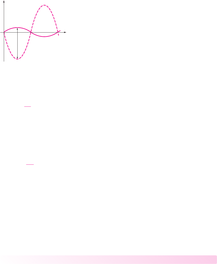
. Assuming sinusoidal signals, Figure 7.48 shows the input signal
v
π
and the output signal
v
o
. As we have noted previously, the output signal is 180 de-
grees out of phase with respect to the input signal. In addition, because of the gain,
the magnitude of the output voltage is larger than the input voltage. The difference
between
v
π
and
v
o
is the voltage across the
C
μ
capacitor as seen in Figure 7.47(a).
7.4.5
r
p
C
p
C
m
g
m
v
p
R
C
v
o
+
–
v
c
+–
v
p
B
E
C
r
p
C
M
C
m
g
m
v
p
R
C
v
o
+
–
v
p
B
E
C
i
c
(a)
(b)
i
c
Figure 7.47 (a) Hybrid-
π
equivalent circuit of a bipolar transistor with a load resistor
R
C
connected to the output. (b) Equivalent circuit with the Miller capacitance.
nea80644_ch07_469-558.qxd 06/13/2009 08:07 PM Page 512 F506 Hard disk:Desktop Folder:Rakesh:MHDQ134-07:
Chapter 7 Frequency Response 513
We may write the sinusoidal signals as
v
π
= V
π
e
jωt
,
v
o
= V
o
e
jωt
,and
v
c
=
V
c
e
jωt
. The current
i
c
through the capacitor
C
μ
can be written as
i
c
= C
μ
dv
c
dt
(7.85(a))
Using phasor notation, we find
I
c
= jωC
μ
V
c
(7.85(b))
This current influences the input impedance looking into the base terminal of the
transistor.
For the two circuits shown in Figures 7.47(a) and 7.47(b) to be equivalent, the
current
i
c
in the two circuits must be the same. From Figure 7.47(b), we can write
i
C
= C
M
dv
π
dt
(7.86(a))
or using phasors, we have
I
c
= jωC
M
V
π
(7.86(b))
For the two capacitor currents in Equations (7.85(b)) and (7.86(b)) to be equal, we
must have
C
μ
V
c
= C
M
V
π
(7.87)
From the signals shown in Figure 7.48, we see that
V
π
< V
c
so that we must
have
C
M
> C
μ
. Because of the 180 degree phase shift and voltage gain, the voltage
across
C
μ
is quite large leading to a relatively significant value of capacitor current
i
c
. In order to have the current in the Miller capacitor
C
M
be the same with a smaller
voltage across
C
M
, the value of
C
M
must be relatively large. This, then, is the physi-
cal origin of the Miller multiplication effect.
Test Your Understanding
TYU 7.6 A bipolar transistor is biased at
I
CQ
= 120 μ
A and its parameters are
β
o
= 120
,
C
μ
= 0.08
pF, and
f
β
= 15
MHz. Determine the capacitance
C
π
. (Ans.
C
π
= 0.328
pF)
v
c
v
p
v
o
t
Figure 7.48 Input signal voltage
v
π
and output signal voltage
v
o
for the circuits in
Figure 7.47
nea80644_ch07_469-558.qxd 06/13/2009 08:07 PM Page 513 F506 Hard disk:Desktop Folder:Rakesh:MHDQ134-07:
514 Part 1 Semiconductor Devices and Basic Applications
TYU 7.7 For the transistor described in Example 7.9 and biased at the same
Q
-point,
determine
h
fe
and the phase at (a)
f = 150
MHz, (b)
f = 500
MHz, and (c)
f = 4
GHz. (Ans. (a)
h
fe
= 89.3
,
φ =−41.9°
; (b)
h
fe
= 38.0
,
φ =−71.5°
;
(c)
h
fe
= 5.0
,
φ =−87.6°)
TYU 7.8 The parameters of a bipolar transistor are:
β
o
= 150
,
f
T
= 1
GHz,
r
π
= 12
k
, and
C
μ
= 0.15
pF. (a) Determine
C
π
and
f
β
. (b) What is the bias cur-
rent in the transistor? (Ans. (a)
C
π
= 1.84
pF,
f
β
= 6.67
MHz; (b)
I
CQ
= 0.325
mA)
7.5 FREQUENCY RESPONSE: THE FET
Objective: • Determine the frequency response of the MOS transis-
tor, and determine the Miller effect and Miller capacitance.
We have considered the expanded hybrid-
π
equivalent circuit of the bipolar transis-
tor that models the high-frequency response of the transistor. We will now develop
the high-frequency equivalent circuit of the FET that takes into account various
capacitances in the device. We will develop the model for a MOSFET, but it also
applies to JFETs and MESFETs.
High-Frequency Equivalent Circuit
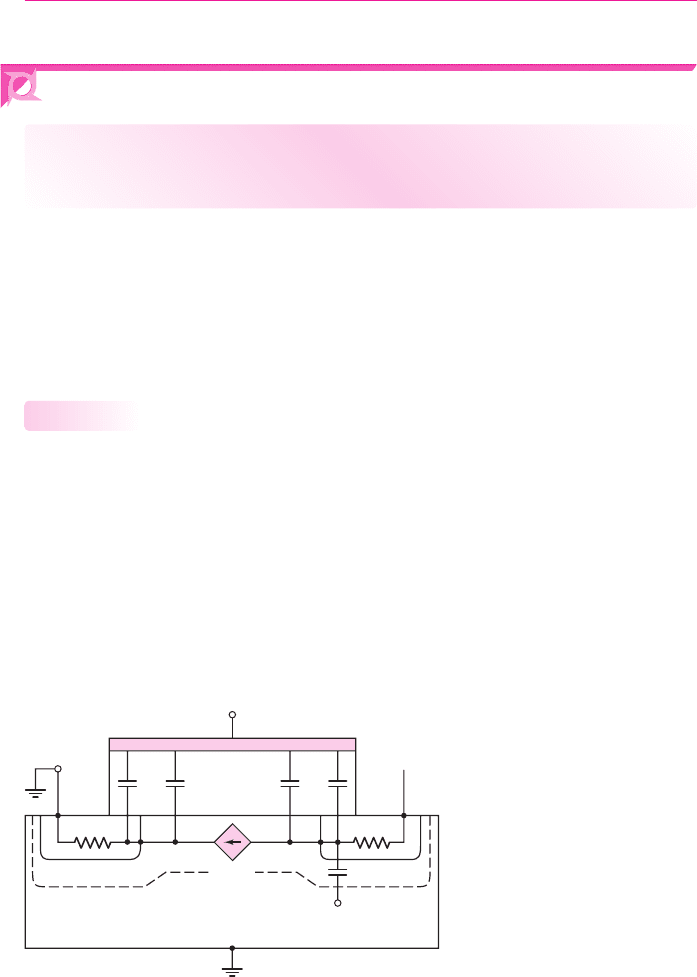
We will construct the small-signal equivalent circuit of a MOSFET from the basic
MOSFET geometry, as described in Chapter 3. Figure 7.49 shows a model based on
the inherent capacitances and resistances in an n-channel MOSFET, as well as the
elements representing the basic device equations. We make one simplifying assump-
tion in the equivalent circuit: The source and substrate are both tied to ground.
Two capacitances connected to the gate are inherent in the transistor. These ca-
pacitances,
C
gs
and
C
gd
, represent the interaction between the gate and the channel
7.5.1
S
D
G
C
gsp
C
gs
C
gd
C
gdp
r
d
C
ds
r
s
n
+
n
+
g
m
V'
gs
p
Figure 7.49 Inherent resistances and capacitances in the n-channel MOSFET structure
nea80644_ch07_469-558.qxd 06/13/2009 08:07 PM Page 514 F506 Hard disk:Desktop Folder:Rakesh:MHDQ134-07:
Chapter 7 Frequency Response 515
inversion charge near the source and drain terminals, respectively. If the device is
biased in the nonsaturation region and
v
DS
is small, the channel inversion charge is
approximately uniform, which means that
C
gs
∼
=
C
gd
∼
=
1
2
WLC
ox
where
C
ox
(F/cm
2
) =
ox
/t
ox
. The parameter
ox
is the oxide permittivity, which for
silicon MOSFETs is
ox
= 3.9
o
, where
o
= 8.85 ×10
−14
F/cm is the permittivity
of free space. The parameter
t
ox
is the oxide thickness in cm.
However, when the transistor is biased in the saturation region, the channel is
pinched off at the drain and the inversion charge is no longer uniform. The value of
C
gd
essentially goes to zero, and
C
gs
approximately equals
(2/3)WLC
ox
. As an ex-
ample, if a device has an oxide thickness of 100 Å, a channel length of
L = 0.18 μ
m,
and a channel width of
W = 20 μ
m, the value of
C
gs
is
C
gs
∼
=
8.3
fF. The value of
C
gs
changes as the device size changes, but typical values are in the tens of femto-
farads range.
The remaining two gate capacitances,
C
gsp
and
C
gdp
, are parasitic or overlap
capacitances, so called because, in actual devices, the gate oxide overlaps the source
and drain contacts, because of tolerances or other fabrication factors. As we will see,
the drain overlap capacitance
C
gdp
lowers the bandwidth of the FET. The parameter
C
ds
is the drain-to-substrate pn junction capacitance, and
r
s
and
r
d
are the series re-
sistances of the source and drain terminals. The internal gate-to-source voltage con-
trols the small-signal channel current through the transconductance.
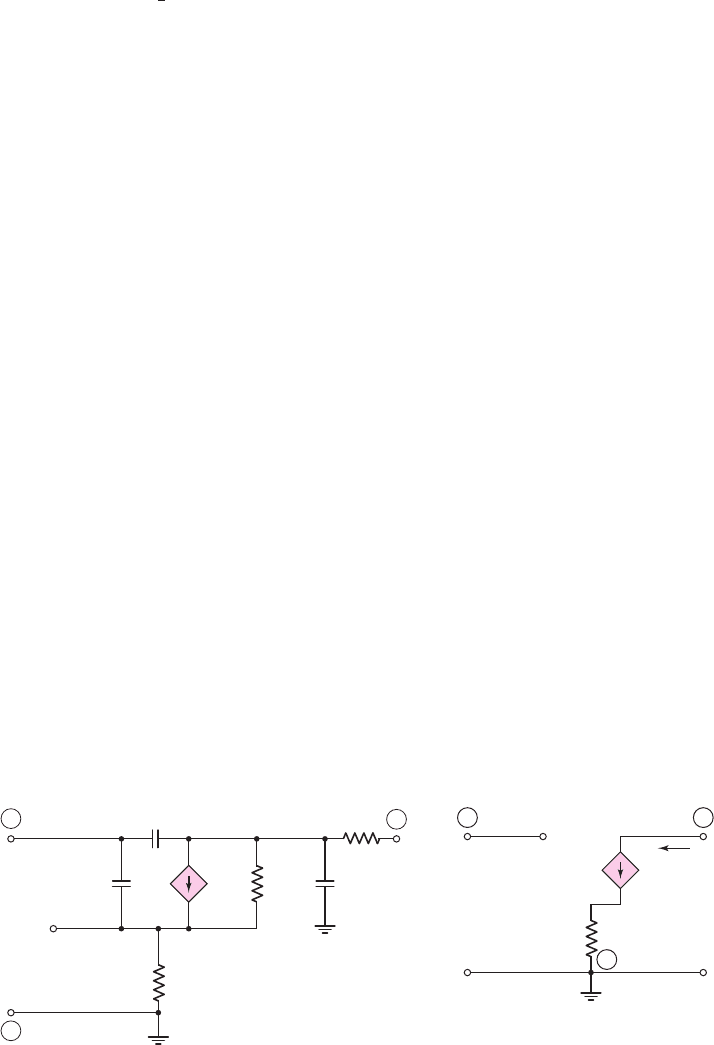
The small-signal equivalent circuit for the n-channel common-source MOSFET
is shown in Figure 7.50. Voltage
V
gs
is the internal gate-to-source voltage that con-
trols the channel current. We will assume that the gate-to-source and gate-to-drain
capacitances,
C
gs
and
C
gd
, contain the parasitic overlap capacitances. One parame-
ter,
r
o
, shown in Figure 7.50 is not shown in Figure 7.49. This resistance is associated
with the slope of
I
D
versus
V
DS
. In the ideal MOSFET biased in the saturation re-
gion,
I
D
is independent of
V
DS
, which means that
r
o
is infinite. However,
r
o
is finite
in short-channel-length devices, because of channel-length modulation, and is there-
fore included in the equivalent circuit.
Source resistance r
s
can have a significant effect on the transistor characteristics.
To illustrate, Figure 7.51 shows a simplified low-frequency equivalent circuit in-
cluding r
s
but not r
o
. For this circuit, the drain current is
I
d
= g
m
V
gs
(7.88)
C
gs
r
o
g
m
V'
gs
C
gd
r
d
+
–
V'
gs
C
ds
D
G
S
+
–
V
gs
r
s
Figure 7.50 Equivalent circuit of the n-channel
common-source MOSFET
I
d
++
–
V
gs
–
r
s
g
m
V'
gs
V'
gs
G D
S
Figure 7.51 Simplified low-frequency
equivalent circuit of the n-channel
common-source MOSFET including
source resistance
r
s
but not resistance
r
o
nea80644_ch07_469-558.qxd 06/13/2009 08:07 PM Page 515 F506 Hard disk:Desktop Folder:Rakesh:MHDQ134-07:
516 Part 1 Semiconductor Devices and Basic Applications
and the relationship between
V
gs
and
V
gs
is
V
gs
= V
gs
+(g
m
V
gs
)r
s
= (1 + g
m
r
s
)V
gs
(7.89)
From Equation (7.88), the drain current can now be written as
I
d
=
g
m
1 + g
m
r
s
V
gs
= g
m
V
gs
(7.90)
Equation (7.90) shows that the source resistance reduces the effective transconduc-
tance, or the transistor gain.
The equivalent circuit of a p-channel MOSFET is exactly the same as that of an
n-channel device, except that all voltage polarities and current directions are re-
versed. The capacitances and resistances are the same for both models.
Unity-Gain Bandwidth
As for the bipolar transistor, the unity-gain frequency or bandwidth is a figure of
merit for the FETs. If we neglect
r
s
,
r
d
,
r
o
,and
C
ds
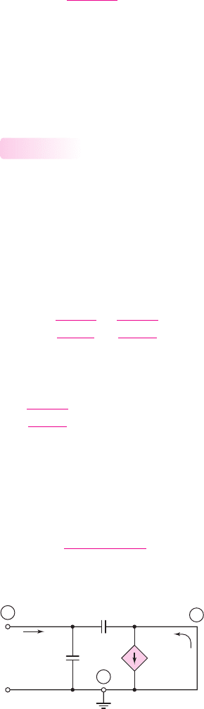
, and connect the drain to signal
ground, the resulting equivalent small-signal circuit is shown in Figure 7.52. Since
the input gate impedance is no longer infinite at high frequency, we can define
the short-circuit current gain. From that we can define and calculate the unity-gain
bandwidth.
Writing a KCL equation at the input node, we find that
I
i
=
V
gs
1
jωC
gs
+
V
gs
1
jωC
gd
= V
gs
[ jω(C
gs
+C
gd
)]
(7.91)
From a KCL equation at the output node, we obtain
V
gs
1
jωC
gd
+ I
d
= g
m
V
gs
(7.92(a))
or
I
d
= V
gs
(g
m
− jωC
gd
)
(7.92(b))
Solving Equation (7.92(b)) for
V
gs
produces
V
gs
=
I
d
(g
m
− jωC
gd
)
(7.93)
7.5.2
C
gs
g
m
V
gs
C
gd
I
d
+
–
V
gs
D
G
S
I
i
Figure 7.52 Equivalent high-frequency small-signal circuit of a MOSFET, for calculating
short-circuit current gain
nea80644_ch07_469-558.qxd 06/13/2009 08:07 PM Page 516 F506 Hard disk:Desktop Folder:Rakesh:MHDQ134-07:

Chapter 7 Frequency Response 517
Substituting Equation (7.93) into (7.91) yields
I
i
= I
d
·
[ jω(C
gs
+C
gd
)]
(g
m
− jωC
gd
)
(7.94)
Therefore, the small-signal current gain is
A
i
=
I
d
I
i
=
g
m
− jωC
gd
jω(C
gs
+C
gd
)
(7.95)
If we assume typical values of
C
gd
= 10
fF and
g
m
= 1
mA/V, and a maximum
frequency of
f = 1
GHz, we find that
ωC
gd
g
m
. The small-signal current gain, to
a good approximation, is then
A
i
=
I
d
I
i
∼
=
g
m
jω(C
gs
+C
gd
)
(7.96)
The unity-gain frequency
f
T
is defined as the frequency at which the magnitude
of the short-circuit current gain goes to 1. From Equation (7.96) we find that
f
T
=
g
m
2π(C
gs
+C
gd
)
(7.97)
The unity-gain frequency or bandwidth is a parameter of the transistor and is inde-
pendent of the circuit.
EXAMPLE 7.11
Objective: Determine the unity-gain bandwidth of an FET.
Consider an n-channel MOSFET with parameters
K
n
= 1.5
mA/V
2
,
V
TN
= 0.4
V,
λ = 0
,
C
gd
= 10
fF, and
C
gs
= 50
fF. Assume the transistor is biased
at
V
GS
= 0.8
V.
Solution: The transconductance is
g
m
= 2K
n
(
V
GS
− V
TN
)
= 2(1.5)
(
0.8 − 0.4
)
= 1.2
mA/V
From Equation (7.97), the unity-gain bandwidth, or frequency, is
f
T
=
g
m
2π(C
gs
+C
gd
)
=
1.2 × 10
−3
2π(50 +10) × 10
−15
= 3.18 ×10
9
Hz
or
f
T
= 3.18 GHz
Comment: As with bipolar transistors, high-frequency FETs require small capaci-
tances and a small device size.
EXERCISE PROBLEM
Ex 7.11: The parameters of an n-channel MOSFET are
K
n
= 1.2
mA/V
2
,
V
TN
= 0.5
V,
λ = 0
,
C
gd
= 8
fF, and
C
gs
= 60
fF. The unity-gain frequency is
found to be
f
T
= 3
GHz. Determine the transconductance and the bias current of
the MOSFET. (Ans.
g
m
= 1.282
mA/V,
I
DQ
= 0.342
mA)
Typically, values of
C
gs
for MOSFETs are in the range of 10 to 50 fF and values
of
C
gd
are typically from 0.1 to 0.5 fF.
nea80644_ch07_469-558.qxd 06/13/2009 08:07 PM Page 517 F506 Hard disk:Desktop Folder:Rakesh:MHDQ134-07: