Neamen D. Microelectronics: Circuit Analysis and Design
Подождите немного. Документ загружается.

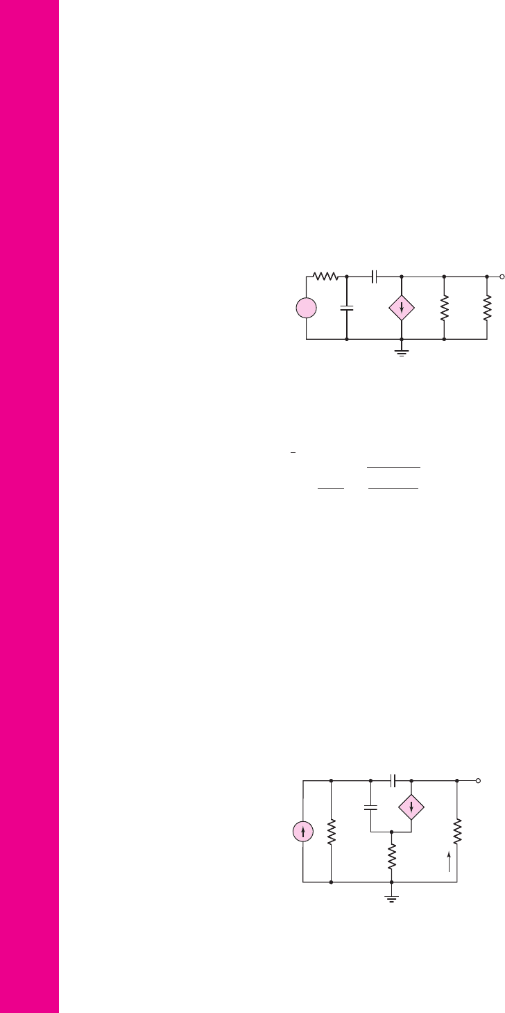
+
–
v
o
v
i
C
C
= 10
m
F
R
S
= 1 kΩ
R
B
= 1 MΩ
R
C
= 5.1 kΩ
C
L
= 10 pF
R
L
=
500 kΩ
V
+
= 12 V
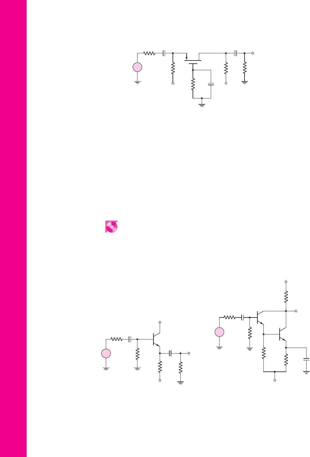
Figure P7.40
548 Part 1 Semiconductor Devices and Basic Applications
D7.36 Consider the circuit in Figure P7.35. The bias voltages are
V
+
= 3
V and
V
−
=−3
V. The transistor parameters are
β = 90
,
V
EB
(on) = 0.7
V and
V
A
=∞
. (a) Design the circuit such that
I
CQ
= 0.15
mA and
V
ECQ
= 2.2
V.
(b) Determine the midband voltage gain. (c) For
C
E
= 3 μ
F, determine the
corner frequencies.
7.37 Consider the common-base circuit in Figure 7.33 in the text. The transistor
parameters are
β = 90
,
V
EB
(on) = 0.7
V, and
V
A
=∞
. A load capacitance
of
C
L
= 3
pF is connected in parallel with
R
L
. (a) Determine the midband
voltage gain. (b) Determine the upper 3 dB frequency.
D7.38 Consider the circuit shown in Figure 7.25(a). The bias voltages are changed
to
V
+
= 3
V and
V
−
=−3
V. The load resistor is
R
L
= 20
k
. The tran-
sistor parameters are
K
p
= 0.1
mA/V
2
,
V
TP
=−0.6
V, and
λ = 0
. (a) De-
sign the circuit such that
I
DQ
= 0.2
mA and
V
SDQ
= 1.9
V. (b) Determine
the value of
C
L
that produces a corner frequency of
f
H
= 4
MHz.
7.39 For the circuit in Figure P7.39, the transistor parameters are:
K
n
=
0.5 mA/V
2
,
V
TN
= 2
V, and
λ = 0
. Determine the maximum value of
C
L
such that the bandwidth is at least
BW = 5
MHz. State any approximations
or assumptions that you make. What is the magnitude of the small-signal
midband voltage gain? Verify the results with a computer simulation.
V
o
v
i
C
C1
=
10
m
F
C
C2
=
10
m
F
C
L
V
DD
= 10 V
R
L
=
4 kΩ
R
i
= 2 kΩ
R
1
= 234 kΩ
R
2
=
166 kΩ
R
S
=
0.5 kΩ
+
–
Figure P7.39
7.40 The parameters of the transistor in the circuit in Figure P7.40 are
β = 100
,
V
BE
(on) = 0.7
V, and
V
A
=∞
. Neglect the capacitance effects of the
transistor. (a) Draw the three equivalent circuits that represent the amplifier
in the low-frequency range, midband range, and the high frequency range.
(b) Sketch the Bode magnitude plot. (c) Determine the values of
|
A
m
|
dB
,
f
L
,
and
f
H
.
7.41 In the common-source amplifier in Figure 7.25(a) in the text, a source bypass
capacitor is to be added between the source terminal and ground potential.
The circuit parameters are
R
S
= 3.2k
,
R
D
= 10 k
,
R
L
= 20 k
, and
C
L
= 10
pF. The transistor parameters are
V
TP
=−2
V,
K
P
= 0.25 mA/V
2
,
and
λ = 0
. (a) Derive the small-signal voltage gain expression, as a function
of
s
, that describes the circuit behavior in the high-frequency range.
(b) What is the expression for the time constant associated with the upper
3 dB frequency? (c) Determine the time constant, upper 3 dB frequency,
and small-signal midband voltage gain.
nea80644_ch07_469-558.qxd 06/13/2009 08:08 PM Page 548 F506 Hard disk:Desktop Folder:Rakesh:MHDQ134-07:
Chapter 7 Frequency Response 549
R
B2
=
10 kΩ
C
B
+
–
v
i
R
B1
=
10 kΩ
C
C2
+10 V
–10 V
R
E1
=
4.7 kΩ
R
E2
=
4.7 kΩ
v
o
+10 V
–10 V
R
C2
= 2.2 kΩ
C
C1
R
S
= 10 kΩ
C
C3
R
L
=
3 kΩ
Q
1
Q
2
+
–
Figure P7.44
v
i
v
o
C
C1
= 1 m F C
C2
= 10 m F
R
S
= 1 kΩ
R
C
=
6.5 kΩ
R
L
=
5 kΩ
R
E
=
10 kΩ
+
–
20 V
+
–
25 V
+
–
Figure P7.42
C
C1
= 1 mF
C
C2
= 1 mF
C
E
= 5
m
F
R
B
= 5 kΩ
R
E
= 1 kΩ
R
S
= 1 kΩ
+4 V
–6 V
v
i
v
o
R
L
=
4 kΩ
R
C
=
4 kΩ
+
–
Figure P7.43
*7.42 Consider the common-base circuit in Figure P7.42. Choose appropriate
transistor parameters. (a) Using a computer analysis, generate the Bode plot
of the voltage gain magnitude from a very low frequency to the midband
frequency range. At what frequency is the voltage gain magnitude 3 dB
below the maximum value? What is the slope of the curve at very low fre-
quencies? (b) Using the PSpice analysis, determine the voltage gain magni-
tude, input resistance
R
i
, and output resistance
R
o
at midband.
*7.43 For the common-emitter circuit in Figure P7.43, choose appropriate transis-
tor parameters and perform a computer analysis. Generate the Bode plot of
the voltage gain magnitude from a very low frequency to the midband fre-
quency range. At what frequency is the voltage gain magnitude 3 dB below
the maximum value? Does one capacitor dominate this 3 dB frequency? If
so, which one?
*7.44 For the multitransistor amplifier in Figure P7.44, choose appropriate tran-
sistor parameters. The lower 3 dB frequency is to be less than or equal to
20 Hz. Assume that all three coupling capacitors are equal. Let
C
B
→∞
.
Using a computer analysis, determine the maximum values of the coupling
capacitors. Determine the slope of the Bode plot of the voltage gain magni-
tude at very low frequencies.
nea80644_ch07_469-558.qxd 06/13/2009 08:08 PM Page 549 F506 Hard disk:Desktop Folder:Rakesh:MHDQ134-07:
550 Part 1 Semiconductor Devices and Basic Applications
Section 7.4 Frequency Response: Bipolar Transistor
7.45 A bipolar transistor has
f
T
= 4
GHz,
β
o
= 120
, and
C
μ
= 0.08
pF when
operated at
I
CQ
= 0.25
mA. Determine
g
m
,
f
β
, and
C
π
.
7.46 A high-frequency bipolar transistor is biased at
I
CQ
= 0.4
mA and has pa-
rameters
C
μ
= 0.075
pF,
f
T
= 2
GHz, and
β
o
= 120
. (a) Determine
C
π
and
f
β
. (b) Determine
h
fe
at (i)
f = 10
MHz, (ii)
f = 20
MHz, and
(iii)
f = 50
MHz.
7.47 (a) The frequency
f
T
of a bipolar transistor is found to be 540 MHz when
biased at
I
CQ
= 0.2
mA. The transistor parameters are
C
μ
= 0.4
pF and
β
o
= 120
. Determine
f
β
and
C
π
. (b) Using the results of part (a), determine
f
T
and
f
β
when the transistor is biased at
I
CQ
= 0.8
mA.
7.48 The circuit in Figure P7.48 is a hybrid-
π
equivalent circuit including the re-
sistance
r
b
. (a) Derive the expression for the voltage gain transfer function
A
v
(s) = V
o
(s)/ V
i
(s)
. (b) If the transistor is biased at
I
CQ
= 1
mA, and if
R
L
= 4
k
and
β
o
= 100
, determine the midband voltage gain for (i)
r
b
=
100
and (ii)
r
b
= 500
. (c) For
C
1
= 2.2
pF, determine the
−3
dB
frequency for (i)
r
b
= 100
and (ii)
r
b
= 500
.
+
–
r
b
R
L
V
o
g
m
V
p
V
i
V
p
r
p
C
1
+
–
Figure P7.48
0.04 V
p
R
L
=
2.5 kΩ
V
i
+
–
V
p
r
p
=
2.5 kΩ
C
p
=
10 pF
r
b
= 200 Ω
C
m
= 0.8 pF
+
–
Figure P7.49
g
m
V
p
R
L
V
i
V
o
+
–
V
p
r
p
C
p
R
S
r
b
C
m
R
B
+
–
Figure P7.50
7.49 Consider the circuit in Figure P7.49. Calculate the impedance seen by the
signal source V
i
at (a)
f = 1
kHz, (b)
f = 10
kHz, (c)
f = 100
kHz, and
(d)
f = 1
MHz.
*7.50 A common-emitter equivalent circuit is shown in Figure P7.50. (a) What is
the expression for the Miller capacitance? (b) Derive the expression for the
voltage gain
A
v
(s) = V
o
(s)/ V
i
(s)
in terms of the Miller capacitance and
other circuit parameters. (c) What is the expression for the upper 3 dB
frequency?
7.51 For the common-emitter circuit in Figure 7.41(a) in the text, assume that
r
s
=∞
,
R
1
R
2
= 5k
, and
R
C
= R
L
= 1
k
. The transistor is biased at
I
CQ
= 5
mA and the parameters are:
β
o
= 200
,
V
A
=∞
,
C
μ
= 5
pF, and
f
T
= 250
MHz. Determine the upper 3 dB frequency for the small-signal
current gain.
nea80644_ch07_469-558.qxd 06/13/2009 08:08 PM Page 550 F506 Hard disk:Desktop Folder:Rakesh:MHDQ134-07:
Chapter 7 Frequency Response 551
*7.52 For the common-emitter circuit in Figure P7.52, assume the emitter bypass
capacitor
C
E
is very large, and the transistor parameters are:
β
o
= 100
,
V
BE
(on) = 0.7
V,
V
A
=∞
,
C
μ
= 2
pF, and
f
T
= 400
MHz. Determine the
lower and upper 3 dB frequencies for the small-signal voltage gain. Use the
simplified hybrid-
π
model for the transistor.
v
i
R
S
= 2 kΩ
C
C1
= 0.1 mF
C
E
→ ∞
+15 V
v
O
R
C
=
4 kΩ
R
E
=
0.2 kΩ
R
1
= 60 kΩ
R
2
= 5.5 kΩ
+
–
Figure P7.52
7.53 Consider the circuit in Figure P7.52. The resistor
R
S
is changed to 500
and all other resistor values are increased by a factor of 10. The transistor
parameters are the same as listed in Problem 7.52. Determine the lower and
upper
−3
dB frequencies for the voltage gain magnitude and find the mid-
band gain.
7.54 The parameters of the circuit shown in Figure P7.52 are changed to
V
+
= 5
V,
R
S
= 0
,
R
1
= 33 k
,
R
2
= 22 k
,
R
C
= 5
k
, and
R
E
= 4k
.
The transistor parameters are
β
o
= 150
,
C
μ
= 0.45
pF, and
f
T
= 800
MHz.
(a) Determine
I
CQ
and
V
CEQ
. (b) Determine
C
π
,
f
β
, and the Miller capaci-
tance
C
M
. (c) Find the upper 3 dB frequency.
Section 7.5 Frequency Response: The FET
7.55 The parameters of an n-channel MOSFET are
k
n
= 80 μA/V
2
,
W = 4 μ
m,
L = 0.8 μ
m,
C
gs
= 50
fF, and
C
gd
= 10
fF. The transistor is biased at
I
DQ
= 0.6
mA. Determine
f
T
.
7.56 Find
f
T
for a MOSFET biased at
I
DQ
= 120 μ
A and
V
GS
− V
TN
= 0.20
V.
The transistor parameters are
C
gs
= 40
fF and
C
gd
= 10
fF.
7.57 Fill in the missing parameter values in the following table for a MOSFET.
Let
K
n
= 1.5
mA/V
2
.
I
D
(μA) f
T
(GHz) C
gs
(fF) C
gd
(fF)
50 60 10
300 60 10
36010
250 2.5 8
nea80644_ch07_469-558.qxd 06/13/2009 08:08 PM Page 551 F506 Hard disk:Desktop Folder:Rakesh:MHDQ134-07:
7.58 (a) An n-channel MOSFET has an electron mobility of 450 cm
2
/V–s and a
channel length of 1.2
μ
m. Let
V
GS
− V
TN
= 0.5V
. Determine the cutoff
frequency
f
T
. (b) Repeat part (a) if the channel length is reduced to
0.18
μ
m.
7.59 A common-source equivalent circuit is shown in Figure P7.59. The transis-
tor transconductance is
g
m
= 3
mA/V. (a) Calculate the equivalent Miller
capacitance. (b) Determine the upper 3 dB frequency for the small-signal
voltage gain.
552 Part 1 Semiconductor Devices and Basic Applications
7.60 Starting with the definition of unity-gain frequency, as given by Equa-
tion (7.97), neglect the overlap capacitance, assume
C
gd
∼
=
0
and
C
gs
∼
=
2
3
WLC
ox
, and show that
f
T
=
3
2π L
·
μ
n
I
D
2C
ox
WL
Since
I
D
is proportional to W, this relationship indicates that to increase
f
T
,
the channel length L must be small.
7.61 The parameters of an ideal n-channel MOSFET are
W/L = 8
,
μ
n
= 400 cm
2
/V–s,
C
ox
= 6.9 ×10
−7
F/cm
2
, and
V
TN
= 0.4
V. (a) Deter-
mine the maximum source resistance such that the transconductance
g
m
is
reduced by no more that 20 percent from its ideal value when
V
GS
= 3
V.
(b) Using the results of part (a), find how much
g
m
is reduced from its ideal
value when
V
GS
= 1
V.
*7.62 Figure P7.62 shows the high-frequency equivalent circuit of an FET, in-
cluding a source resistance r
s
. (a) Derive an expression for the low-
frequency current gain
A
i
= I
o
/I
i
. (b) Assuming R
i
is very large, derive an
expression for the current gain transfer function
A
i
(s) = I
o
(s)/I
i
(s)
.
(c) How does the magnitude of the current gain behave as r
s
increases?
g
m
V
gs
R
D
=
10 kΩ
r
o
=
120 kΩ
V
i
V
o
r
i
= 10 kΩ
+
–
C
gd
= 12 fF
C
gs
=
80 fF
+
–
V
gs
+
–
Figure P7.59
Figure P7.62
g
m
V
gs
R
L
C
gs
C
gd
I
i
V
o
r
s
R
i
+
–
V
gs
I
o
nea80644_ch07_469-558.qxd 06/13/2009 08:08 PM Page 552 F506 Hard disk:Desktop Folder:Rakesh:MHDQ134-07:
Chapter 7 Frequency Response 553
Section 7.6 High-Frequency Response of Transistor Circuits
7.64 The midband voltage gain of a common-source MOSFET amplifier is
A
v
=−15
V/V. The capacitances of the transistor are
C
gs
= 0.2
pF and
C
gd
= 0.04
pF. (a) Determine the input Miller capacitance. (b) What equiv-
alent input resistance (bias resistance and signal source resistance) would
result in an upper corner frequency of 5 MHz?
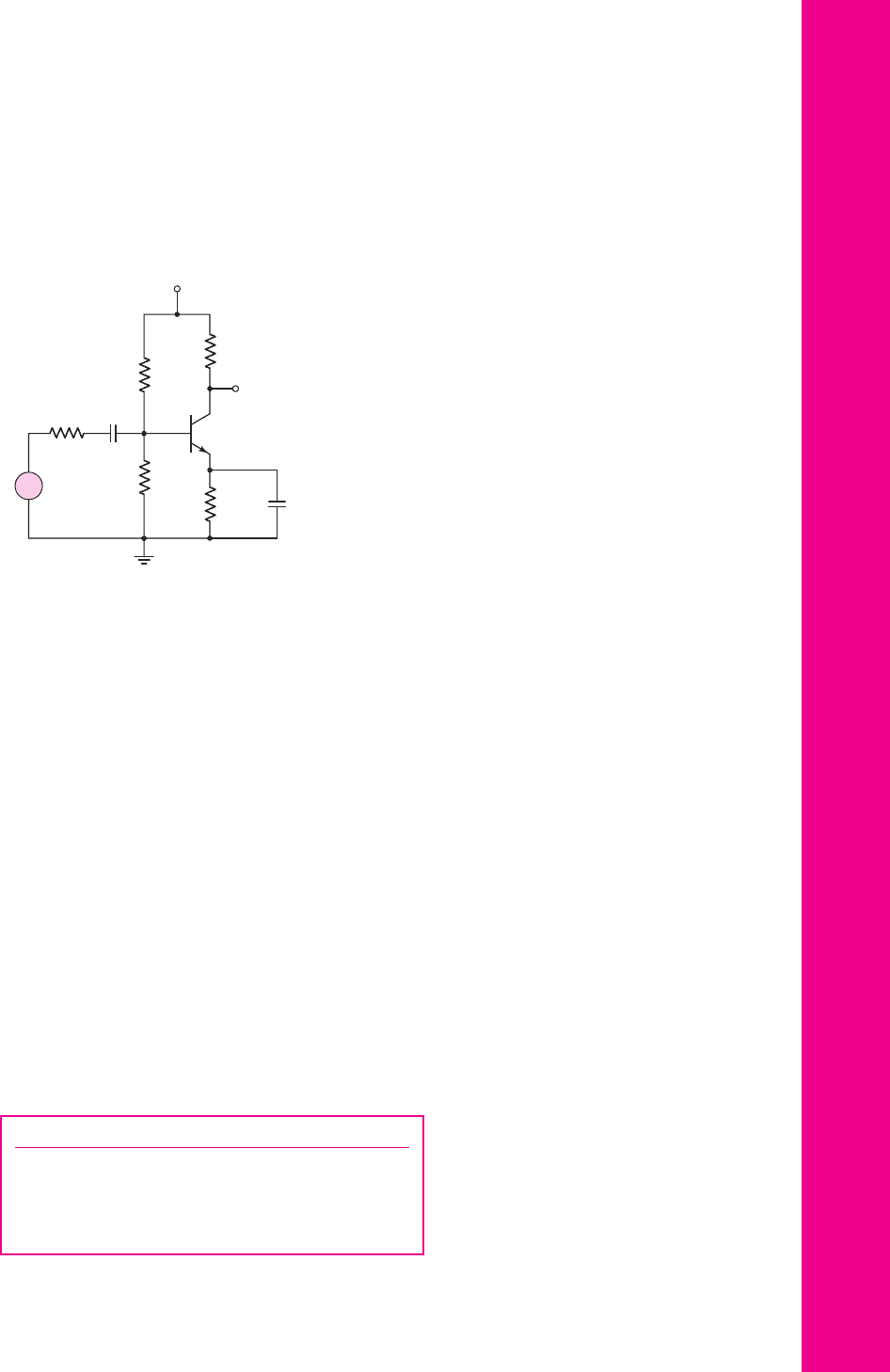
7.65 In the circuit in Figure P7.65, the transistor parameters are:
β = 120
,
V
BE
(on) = 0.7
V,
V
A
= 100
V,
C
μ
= 1
pF, and
f
T
= 600
MHz. (a) Deter-
mine
C
π
and the equivalent Miller capacitance
C
M
. State any approxima-
tions or assumptions that you make. (b) Find the upper 3 dB frequency and
the midband voltage gain.
Figure P7.63
Figure P7.65
v
i
R
i
= 1 kΩ
C
C
= 10 mF
V
DD
= +10 V
v
O
R
D
=
5 kΩ
R
1
= 500 kΩ
R
2
= 225 kΩ
+
–
v
i
R
S
= 2 kΩ
C
C1
= 1 m F
C
C2
= 2 mF
C
E
=
10 mF
+5 V
v
o
R
C
= 4 kΩ
R
1
= 33 kΩ
R
2
= 22 kΩ
R
E
=
4 kΩ
R
L
=
5 kΩ
+
–
7.63 For the FET circuit in Figure P7.63, the transistor parameters are:
K
n
=
1 mA/V
2
,
V
TN
= 2
V,
λ = 0
,
C
gs
= 50
fF, and
C
gd
= 8
fF. (a) Draw the
simplified high-frequency equivalent circuit. (b) Calculate the equivalent
Miller capacitance. (c) Determine the upper 3 dB frequency for the small-
signal voltage gain and find the midband voltage gain.
nea80644_ch07_469-558.qxd 06/13/2009 08:08 PM Page 553 F506 Hard disk:Desktop Folder:Rakesh:MHDQ134-07:
554 Part 1 Semiconductor Devices and Basic Applications
7.67 The parameters of the transistor in the common-source circuit in Fig-
ure P7.67 are:
K
p
= 2
mA/V
2
,
V
TP
=−2
V,
λ = 0.01 V
−1
,
C
gs
= 10
pF,
and
C
gd
= 1
pF. (a) Determine the equivalent Miller capacitance
C
M
.
(b) Find the upper 3 dB frequency and midband voltage gain.
Figure P7.67
v
i
R
G
=
100 kΩ
R
i
= 2 kΩ
C
S
+9 V
–9 V
R
D
= 1 kΩ
R
S
= 1.2 kΩ
v
O
+
–
Figure P7.66
v
i
R
S
= 0.5 kΩ
C
C1
= 4.7 mF
v
o
R
C
= 5 kΩ
V
CC
= +10 V
R
1
= 40 kΩ
R
2
= 5 kΩ
R
E
=
0.5 kΩ
C
E
→ ∞
C
C2
→ ∞
R
L
=
2.5 kΩ
+
–
7.68 The bias voltages of the circuit shown in Figure P7.67 are changed to
V
+
= 3
V and
V
−
=−3
V. The input resistances are
R
i
= 4k
and
R
G
= 200
k
. The transistor parameters are
K
p
= 0.5
mA/V
2
,
V
TP
=
−0.5
V,
λ = 0
,
C
gs
= 0.8
pF, and
C
gd
= 0.08
pF. (a) Design the circuit such
that
I
DQ
= 0.5
mA and
V
SDQ
= 2
V. (b) Find the midband voltage gain.
(c) Determine the equivalent Miller capacitance. (d) Find the upper 3 dB
frequency.
*7.66 In the circuit in Figure P7.66, the transistor parameters are:
β = 120
,
V
BE
(on) = 0.7
V,
V
A
=∞
,
C
μ
= 3
pF, and
f
T
= 250
MHz. Assume the
emitter bypass capacitor
C
E
and the coupling capacitor
C
C2
are very large.
(a) Determine the lower and upper 3 dB frequencies. Use the simplified
hybrid-
π
model for the transistor. (b) Sketch the Bode plot of the voltage
gain magnitude.
nea80644_ch07_469-558.qxd 06/13/2009 08:08 PM Page 554 F506 Hard disk:Desktop Folder:Rakesh:MHDQ134-07:
Chapter 7 Frequency Response 555
7.69 For the PMOS common-source circuit shown in Figure P7.69, the transistor
parameters are:
V
TP
=−2V
,
K
p
= 1
mA/V
2
,
λ = 0
,
C
gs
= 15
pF, and
C
gd
= 3
pF. (a) Determine the upper 3 dB frequency. (b) What is the equiv-
alent Miller capacitance? State any assumptions or approximations that you
make. (c) Find the midband voltage gain.
Figure P7.69
Figure P7.70
Figure P7.72Figure P7.71
C
C1
= 2 mF
C
C2
= 2 mF
C
S
= 10 mF
R
2
= 22 kΩ
R
1
= 8 kΩ
R
i
= 0.5 kΩ
+10 V
–10 V
v
o
R
L
=
5 kΩ
R
D
=
2 kΩ
R
S
= 0.5 kΩ
v
i
+
–
+
–
+5 V
C
B
R
S
= 50 Ω
R
E
=
0.5 kΩ
R
B
= 100 kΩ
I
Q
= 0.5 mA
v
i
R
L
=
1 kΩ
v
o
C
C1
C
C2
+
–
+
–
25 V
+
–
20 V
C
C1
R
S
= 1 kΩ
R
E
=
10 kΩ
R
C
=
6.5 kΩ
v
i
R
L
=
5 kΩ
v
o
C
C2
+
–
v
i
v
o
R
i
= 2 kΩ
R
L
=
4 kΩ
R
D
=
5 kΩ
R
S
=
10 kΩ
V
–
= –5 V V
+
= +5 V
C
C1
= 1 mF C
C2
= 2 mF
+
–
*7.72 In the common-gate circuit in Figure P7.72, the transistor parameters are:
V
TN
= 1
V,
K
n
= 3
mA/V
2
,
λ = 0
,
C
gs
= 15
pF, and
C
gd
= 4
pF. Deter-
mine the upper 3 dB frequency and midband voltage gain.
7.73 Consider the common-gate circuit in Figure P7.73 with parameters
V
+
=
5V,
V
−
=−5V
,
R
S
= 4k
,
R
D
= 2k
,
R
L
= 4k
,
R
G
= 50 k
, and
*7.70 In the common-base circuit shown in Figure P7.70, the transistor parame-
ters are:
β = 100
,
V
BE
(on) = 0.7
V,
V
A
=∞
,
C
π
= 10
pF, and
C
μ
= 1
pF.
(a) Determine the upper 3 dB frequencies corresponding to the input and
output portions of the equivalent circuit. (b) Calculate the small-signal mid-
band voltage gain. (c) If a load capacitor
C
L
= 15
pF is connected between
the output and ground, determine if the upper 3 dB frequency will be dom-
inated by the
C
L
load capacitor or by the transistor characteristics.
*7.71 Repeat Problem 7.70 for the common-base circuit in Figure P7.71. Assume
V
EB
(on) = 0.7
for the pnp transistor. The remaining transistor parameters
are the same as given in Problem 7.70.
nea80644_ch07_469-558.qxd 06/13/2009 08:08 PM Page 555 F506 Hard disk:Desktop Folder:Rakesh:MHDQ134-07:
556 Part 1 Semiconductor Devices and Basic Applications
Figure P7.75
Figure P7.76
v
i
R
B
=
100 kΩ
C
C2
+10 V
–10 V
R
E
=
10 kΩ
v
o
R
L
C
C1
R
S
= 2 kΩ
+
–
C
E
C
C
v
O
v
i
Q
1
Q
2
+10 V
R
E2
=
10 kΩ
R
E1
R
C
= 2 kΩ
R
B
=
20 kΩ
R
S
= 1 kΩ
–10 V
+
–
R
i
= 0.5k
. The transistor parameters are:
K
p
= 1
mA/V
2
,
V
TP
=
−0.8V
,
λ = 0
,
C
gs
= 4
pF, and
C
gd
= 1
pF. Determine the upper 3 dB
frequency and midband voltage gain.
*7.74 For the cascode circuit in Figure 7.65 in the text, circuit parameters are the
same as described in Example 7.15. The transistor parameters are:
β
o
= 120
,
V
A
=∞
,
V
BE
(on) = 0.7
V,
C
π
= 12
pF, and
C
μ
= 2
pF. (a) If
C
L
is an open circuit, determine the 3 dB frequencies corresponding to the
input and output portions of the equivalent circuit. (b) Determine the mid-
band voltage gain. (c) If a load capacitance
C
L
= 15
pF is connected to the
output, determine if the upper 3 dB frequency is dominated by the load
capacitance or by the transistor characteristics.
COMPUTER SIMULATION PROBLEMS
7.75 An emitter-follower amplifier is shown in Figure P7.75. Using a computer
simulation, determine the upper 3 dB frequency and the midband voltage
gain for: (a)
R
L
= 0.2
k
, (b)
R
L
= 2
k
, and (c)
R
L
= 20
k
. Use a
standard transistor. Explain any differences between the results of the
three parts.
Figure P7.73
v
i
v
o
R
i
R
L
R
D
R
S
R
G
C
G
V
–
V
+
C
C1
C
C2
+
–
7.76 The transistor circuit in Figure P7.76 is a Darlington pair configuration.
Using a computer simulation, determine the upper 3 dB frequency and the
nea80644_ch07_469-558.qxd 06/13/2009 08:08 PM Page 556 F506 Hard disk:Desktop Folder:Rakesh:MHDQ134-07:
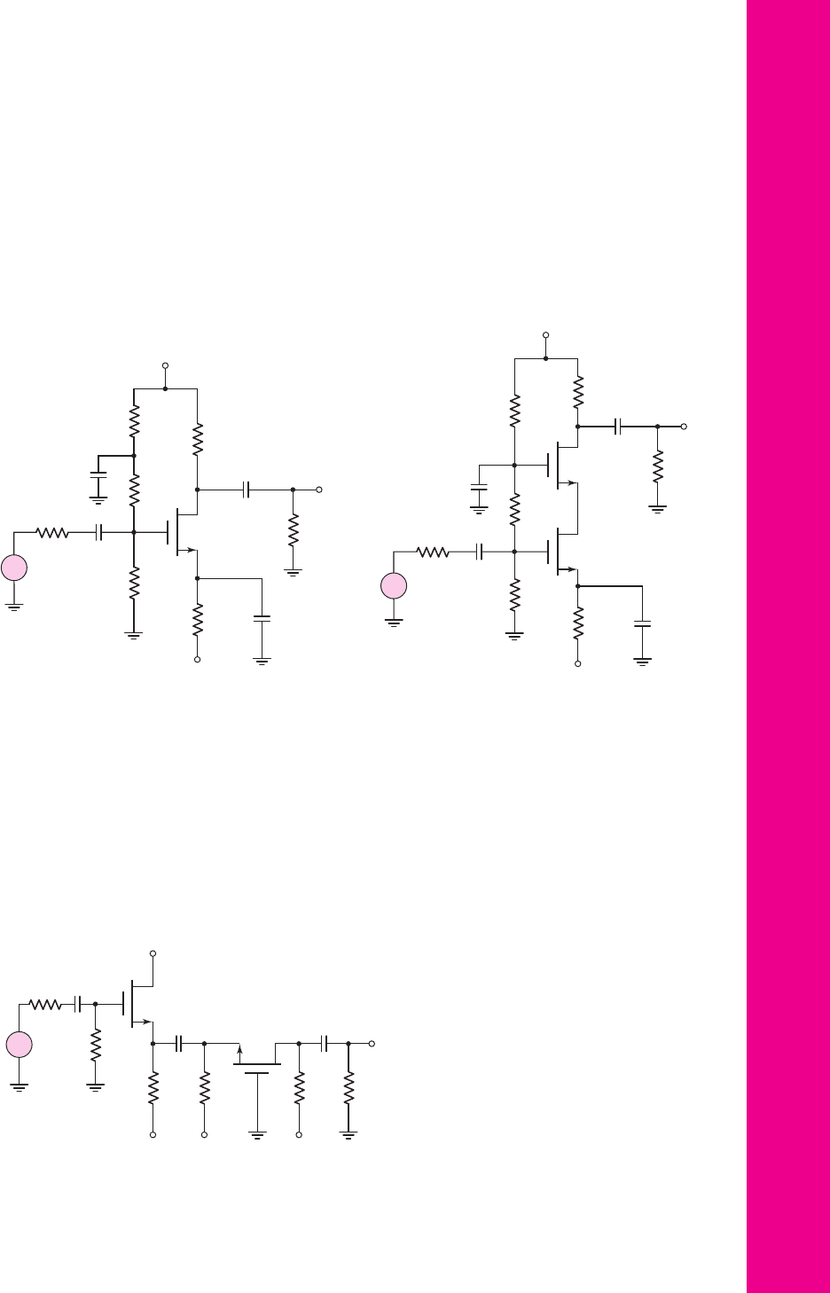
7.78 Consider identical transistors in the circuit in Figure P7.78. Assume the two
coupling capacitors are both equal to
C
C
= 4.7 μ
F. Using a computer sim-
ulation, determine the lower and upper 3 dB frequencies as well as the mid-
band gain. What value of load capacitance will change the bandwidth by a
factor of two?
Chapter 7 Frequency Response 557
Figure P7.78
Figure P7.77
C
S
C
C1
C
G
C
C2
R
3
= 145.5 kΩ
R
1
= 179.5 kΩ
R
i
= 2 kΩ
V
–
= –10 V
v
o
R
L
= 10 kΩ
R
D
= 3 kΩ
V
+
= +10 V
R
2
=
175 kΩ
v
i
R
S
=
10 kΩ
(a)
+
–
(b)
C
S
C
C1
C
G
C
C2
R
3
= 145.5 kΩ
R
1
= 179.5 kΩ
R
i
= 2 kΩ
V
–
= –10 V
v
o
R
L
=
10 kΩ
R
D
= 3 kΩ
R
2
=
175 kΩ
v
i
R
S
=
10 kΩ
M
2
M
1
V
+
= +10 V
+
–
v
i
R
G
=
400 kΩ
+10 V
–10 V –10 V
+10 V
R
S1
=
10 kΩ
R
S2
=
10 kΩ
v
o
R
D
=
5 kΩ
R
L
=
2 kΩ
C
C1R
i
= 2 kΩ
M
1
M
2
C
C2
C
C3
+
–
midband voltage gain for (a)
R
E1
= 10
k
,(b)
R
E1
= 40
k
, and
(c)
R
E1
=∞
. Use standard transistors. Explain any differences between
the results of the three parts.
7.77 Consider the common-source amplifier in Figure P7.77(a) and the cascode
amplifier in Figure P7.77(b). Using standard transistors, determine the upper
3 dB frequency and the midband voltage gain for each circuit using a com-
puter simulation. Compare the 3 dB frequencies and midband voltage gains.
nea80644_ch07_469-558.qxd 06/13/2009 08:08 PM Page 557 F506 Hard disk:Desktop Folder:Rakesh:MHDQ134-07: