Neamen D. Microelectronics: Circuit Analysis and Design
Подождите немного. Документ загружается.


568 Part 1 Semiconductor Devices and Basic Applications
(a) (b) (c)
Figure 8.10 Two packaging schemes: (a) and (b) for power transistors and (c) typical
heat sink
where P is the thermal power through the element. Temperature difference is the
electrical analog of voltage, and power or heat flow is the electrical analog of
current.
Manufacturers’ data sheets for power devices generally give the maximum
operating junction or device temperature T
j,max
and the thermal resistance from the
junction to the case
θ
jc
= θ
dev−case
.
2
By definition, the thermal resistance between the
case and heat sink is
θ
case−snk
, and between the heat sink and ambient is
θ
snk−amb
.
The temperature difference between the device and the ambient can now be
written as follows, when a heat sink is used:
T
dev
− T
amb
= P
D
(θ
dev−case
+θ
case−snk
+θ
snk−amb
)
(8.6)
where P
D
is the power dissipated in the device. Equation (8.6) may also be modeled
by its equivalent electrical elements, as shown in Figure 8.11. The temperature
difference across the elements, such as the case and heat sink, is the dissipated
power P
D
multiplied by the applicable thermal resistance, which is
θ
case−snk
for this
example.
If a heat sink is not used, the temperature difference between the device and
ambient is written as
T
dev
− T
amb
= P
D
(θ
dev−case
+θ
case−amb
)
(8.7)
where
θ
case−amb
is the thermal resistance between the case and ambient.
EXAMPLE 8.2
Objective: Determine the maximum power dissipation in a transistor and determine
the temperature of the transistor case and heat sink.
Consider a power MOSFET for which the thermal resistance parameters are:
θ
dev−case
= 1.75
◦
C/W θ
case−snk
= 1
◦
C/W
θ
snk−amb
= 5
◦
C/W θ
case−amb
= 50
◦
C/W
The ambient temperature is
T
amb
= 30
°C, and the maximum junction or device
temperature is
T
j,max
= T
dev
= 150
°C.
2
In this short discussion, we use a more descriptive subscript notation to help clarify the discussion.
T
dev
T
case
T
snk
T
amb
P
D
q
dev-case
q
case-snk
q
snk-amb
Figure 8.11 Electrical
equivalent circuit for heat
flow from the device to the
ambient
nea80644_ch08_559-614.qxd 06/15/2009 01:31 PM Page 568 F506 Hard disk:Desktop Folder:ALI:MHDQ134-08 Folder:MHDQ134-08:

Chapter 8 Output Stages and Power Amplifiers 569
Solution (Maximum Power): When no heat sink is used, the maximum device power
dissipation is found from Equation (8.7) as
P
D,max
=
T
j,max
− T
amb
θ
dev−case
+θ
case−amb
=
150 − 30
1.75 + 50
= 2.32 W
When a heat sink is used, the maximum device power dissipation is found from
Equation (8.6) as
P
D,max
=
T
j,max
− T
amb
θ
dev−case
+θ
case−snk
+θ
snk−amb
=
150 − 30
1.75 + 1 +5
= 15.5W
Solution (Temperature): The device temperature is
T = 150
°C and the ambient
temperature is
T
amb
= 30
°C. The heat flow is
P
D
= 15.5
W. The heat sink tempera-
ture (see Figure 8.11) is found from
T
snk
− T
amb
= P
D
· θ
snk−amb
or
T
snk
= 30 +(15.5)(5) ⇒ T
snk
= 107.5
◦
C
The case temperature is found from
T
case
− T
amb
= P
D
· (θ
case−snk
+θ
snk−case
)
or
T
case
= 30 +(15.5)(1 +5) ⇒ T = 123
◦
C
Comment: These results illustrate that the use of a heat sink allows more power to
be dissipated in the device, while keeping the device temperature at or below its
maximum limit.
EXERCISE PROBLEM
Ex 8.2: A power BJT is operating with an average collector current of
I
C
= 2
A
and an average collector–emitter voltage of
V
CE
= 8
V. The device parameters are
θ
dev−case
= 3
◦
C/W,
θ
case−snk
= 1
◦
C/W, and
θ
snk−amb
= 4
◦
C/W. The ambient
temperature is
25
◦
C. Determine the temperatures of the (a) device, (b) case, and
(c) heat sink. (Ans. (a)
153
◦
C, (b)
105
◦
C, (c)
89
◦
C)
The maximum safe power dissipation in a device is a function of: (1) the
temperature difference between the junction and case, and (2) the thermal resistance
between the device and the case
θ
dev−case
,or
P
D,max
=
T
j,max
− T
case
θ
dev−case
(8.8)
A plot of P
D,max
versus T
case
, called the power derating curve of the transistor,
is shown in Figure 8.12. The temperature at which the power derating curve crosses
the horizontal axis corresponds to T
j, max
. At this temperature, no additional tempera-
ture rise in the device can be tolerated; therefore, the allowed power dissipation must
be zero, which implies a zero input signal.
nea80644_ch08_559-614.qxd 06/15/2009 01:31 PM Page 569 F506 Hard disk:Desktop Folder:ALI:MHDQ134-08 Folder:MHDQ134-08:

570 Part 1 Semiconductor Devices and Basic Applications
The rated power of a device is generally defined as the power at which the
device reaches its maximum temperature, while the case temperature remains at
room or ambient temperature, that is,
T
case
= 25
°C. Maintaining the case at ambient
temperature implies that the thermal resistance between the case and ambient is zero,
or that an infinite heat sink is used. However, an infinite heat sink is not possible.
With nonzero values of
θ
case−snk
and
θ
snk−amb
, the case temperature rises above the
ambient, and the maximum rated power of the device cannot be achieved. This effect
can be seen by examining the equivalent circuit model in Figure 8.11. If the device
temperature is at its maximum allowed value of T
dev
= T
j,max
, then as T
case
in-
creases, the temperature difference across
θ
dev−case
decreases, which means that
the power through the element must decrease.
EXAMPLE 8.3
Objective: Determine the maximum safe power dissipation in a transistor.
Consider a BJT with a rated power of 20 W and a maximum junction tempera-
ture of
T
j,max
= 175
◦
C. The transistor is mounted on a heat sink with parameters
θ
case−snk
= 1
◦
C/W
and
θ
snk−amb
= 5
◦
C/W
.
Solution: From Equation (8.8), the device-to-case thermal resistance is
θ
dev−case
=
T
j,max
− T
OC
P
D,rated
=
175 − 25
20
= 7.5
◦
C/W
From Equation (8.6), the maximum power dissipation is
P
D,max
=
T
j,max
− T
amb
θ
dev−case
+θ
case−snk
+θ
snk−amb
=
175 − 25
7.5 + 1 +5
= 11.1W
Comment: The actual maximum safe power dissipation in a device may be less than
the rated value. This occurs when the case temperature cannot be held at the ambient
temperature, because of the nonzero thermal resistance factors between the case and
ambient.
P
D,
max
T
case
T
OC
= 25 °C T
j, max
P
D, rated
Figure 8.12 A power derating curve
nea80644_ch08_559-614.qxd 06/15/2009 01:31 PM Page 570 F506 Hard disk:Desktop Folder:ALI:MHDQ134-08 Folder:MHDQ134-08:

Chapter 8 Output Stages and Power Amplifiers 571
EXERCISE PROBLEM
Ex 8.3: The rated power of a power BJT is
P
D,rated
= 50
W, the maximum
allowed junction temperature is
T
j,max
= 200
°C, and the ambient temperature is
T
amb
= 25
◦
C. The thermal resistance between the heat sink and air is
θ
snk−amb
=
2
◦
C/W
, and that between the case and heat sink is
θ
case−snk
= 0.5
◦
C/W
. Find the
maximum safe power dissipation and the temperature of the case. (Ans.
P
D,max
=
29.2 W,
T
case
= 98
°C)
Test Your Understanding
TYU 8.1 Consider the common-source circuit shown in Figure 8.13. The parameters
are
R
D
= 20
and
V
DD
= 24
V. Determine the required current, voltage, and power
ratings of the MOSFET. (Ans.
I
D
(max) = 1.2
A,
V
DS
(max) = 24
V,
P
D
(max) =
7.2 W)
TYU 8.2 The emitter-follower circuit shown in Figure 8.14 is biased with
V
CC
= 12
V.
The transistor current gain is
β = 80
, and the transistor limiting factors are
I
C,max
= 250
mA and
V
CE
(
sus
)
= 30
V. The transistor
Q
-point is to remain within the
safe operating area at all times. (a) Determine the minimum value of
R
E
. (b) Determine
the minimum required transistor power rating. (Ans. (a)
R
E
= 96
, (b)
P
Q
= 1.5
W)
TYU 8.3 (a) Assume the power flow through a material with a thermal resistance pa-
rameter of
θ = 1.8
◦
C/W is
P = 6
W. Determine the resulting temperature difference
across the material. (b) The thermal resistance of a material is
θ = 2.5
◦
C/W. If the
temperature difference across the material is
T = 100
◦
C, find the power flow
through the material. (Ans. (a)
T = 10.8
◦
C, (b)
P = 40
W)
R
D
I
D
V
i
+
–
V
DS
V
DD
Figure 8.13 Figure for
Exercise TYU 8.1 and
Example 8.4
R
E
v
I
v
O
–V
CC
+V
CC
Figure 8.14 Figure for
Exercise TYU 8.2
8.3 CLASSES OF AMPLIFIERS
Objective: • Define various classes of power amplifiers, and investi-
gate the characteristics, including power efficiency, of a few of these
amplifiers.
nea80644_ch08_559-614.qxd 06/15/2009 01:31 PM Page 571 F506 Hard disk:Desktop Folder:ALI:MHDQ134-08 Folder:MHDQ134-08:

572 Part 1 Semiconductor Devices and Basic Applications
Some power amplifiers are classified according to the percent of time the output
transistors are conducting, or “turned on.” Four of the principal classifications are:
class A, class B, class AB, and class C. These classifications are illustrated in Fig-
ure 8.15 for a sinusoidal input signal. In class-A operation, an output transistor is
biased at a quiescent current
I
Q
and conducts for the entire cycle of the input signal.
For class-B operation, an output transistor conducts for only one-half of each sine
wave input cycle. In class-AB operation, an output transistor is biased at a small
quiescent current
I
Q
and conducts for slightly more than half a cycle. In contrast, in
class-C operation an output transistor conducts for less than half a cycle. These
four types of power amplifiers use the output transistors as a current source. We will
analyze the biasing, load lines, and power efficiency of each class of these power
amplifiers.
Another classification of power amplifiers, including class D, class E, and class
F, uses the output transistors as switches. The output of the amplifier is, in general, a
high-
Q
resonant RLC circuit. When the switch is closed, current and power are sup-
plied to the output resonant circuit. In the ideal case, when the switch is closed, there
is zero voltage across the switch, and when the switch is open, there is zero current
through the switch. In both cases, the ideal power dissipated in the switch is zero. The
power efficiency of these amplifiers can then approach 100 percent.
The intent of this chapter is to provide the basic characteristics of a few of these
power amplifiers. As usual, there are other types of power amplifiers and power elec-
tronics that are beyond the scope of this text, including high-frequency radio-frequency
(RF) circuit design.
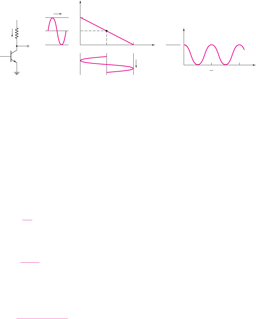
Class-A Operation
The small-signal amplifiers considered in Chapters 4 and 6 were all biased for
class-A operation. A basic common-emitter configuration is shown in Figure 8.16(a).
The bias circuitry has been omitted, for convenience. Also, in this standard class-A
amplifier configuration, no inductors or transformers are used.
8.3.1
i
C
p
I
CQ
0 2p 3p 4p
p
2p 3p 4p
p
2p 3p 4p
p
2p 3p 4p
ω
t
i
C
0
ω
t
i
C
I
CQ
0
ω
t
i
C
0
ω
t
(a) (b)
(c) (d)
Figure 8.15 Collector current versus time characteristics: (a) class-A amplifier, (b) class-B
amplifier, (c) class-AB amplifier, and (d) class-C amplifier
nea80644_ch08_559-614.qxd 06/15/2009 01:31 PM Page 572 F506 Hard disk:Desktop Folder:ALI:MHDQ134-08 Folder:MHDQ134-08:
Chapter 8 Output Stages and Power Amplifiers 573
The dc load line is shown in Figure 8.16(b). The Q-point is assumed to be in the
center of the load line, so that
V
CEQ
= V
CC
/2
. If a sinusoidal input signal is applied,
sinusoidal variations are induced in the collector current and collector–emitter volt-
age. The absolute possible variations are shown in the figure, although values of
v
CE
= 0
and
i
C
= 2I
CQ
cannot actually be attained.
The instantaneous power dissipation in the transistor, neglecting the base
current, is
p
Q
= v
CE
i
C
(8.9)
For a sinusoidal input signal, the collector current and collector-emitter voltage can
be written
i
C
= I
CQ
+ I
p
sin ωt
(8.10(a))
and
v
CE
=
V
CC
2
− V
p
sin ωt
(8.10(b))
If we consider the absolute possible variations, then
I
p
= I
CQ
and
V
p
= V
CC
/2
.
Therefore, the instantaneous power dissipation in the transistor, from Equa-
tion (8.9), is
p
Q
=
V
CC
I
CQ
2
(1 − sin
2
ωt)
(8.11)
Figure 8.16(c) is a plot of the instantaneous transistor power dissipation. Since
the maximum power dissipation corresponds to the quiescent value (see Figure 8.5),
the transistor must be capable of handling a continuous power dissipation of
V
CC
I
CQ
/2
when the input signal is zero.
The power conversion efficiency is defined as
η =
signal load power(
¯
P
L
)
supply power(
¯
P
S
)
(8.12)
where
¯
P
L
is the average ac power delivered to the load and
¯
P
S
is the average power
supplied by the V
CC
power source(s). For the standard class-A amplifier and
R
L
i
C
v
I
v
O
+
–
V
CC
v
CE
i
C
v
CE
V
CC
V
CEQ
I
CQ
2I
CQ
Q-point
DC load line
Time
Time
0
0
T
T
P
Q
Time
0
T
2
T
V
CC
I
CQ
2
(a) (b) (c)
Figure 8.16 (a) Common-emitter amplifier, (b) dc load line, and (c) instantaneous power
dissipation versus time in the transistor
nea80644_ch08_559-614.qxd 06/15/2009 01:31 PM Page 573 F506 Hard disk:Desktop Folder:ALI:MHDQ134-08 Folder:MHDQ134-08:

574 Part 1 Semiconductor Devices and Basic Applications
sinusoidal input signals, the average ac power delivered to the load is
1
2
V
p
I
p
. Using
the absolute possible variations, we have
¯
P
L
(max) =
1
2
V
CC
2
(I
CQ
) =
V
CC
I
CQ
4
(8.13)
The average power supplied by the V
CC
source is
¯
P
S
= V
CC
I
CQ
(8.14)
The maximum attainable conversion efficiency is therefore
η(max) =
1
4
V
CC
I
CQ
V
CC
I
CQ
⇒ 25%
(8.15)
We must keep in mind that the maximum possible conversion efficiency may change
when a load is connected to the output of the amplifier. This efficiency is relatively
low; therefore, standard class-A amplifiers are normally not used when signal powers
greater than approximately 1 W are required.
We must also emphasize that in practice, a maximum signal voltage of
V
CC
/2
and
a maximum signal current of I
CQ
are not possible. The output signal voltage must be lim-
ited to smaller values in order to avoid transistor saturation and cutoff, and the resulting
nonlinear distortion. The calculation for the maximum possible efficiency also neglects
power dissipation in the bias circuitry. Consequently, the realistic maximum conversion
efficiency in a standard class-A amplifier is on the order of 20 percent or less.
Design Pointer: In circuit analysis, the maximum power transfer theorem stated that
the load impedance should be matched to the amplifier output impedance, which pro-
vides a 50 percent power conversion efficiency. However, in the design of power am-
plifiers, this theorem is not practical. For example, if 50 kW is to be delivered to an
antenna, then the circuit would also dissipate 50 kW if the power conversion effi-
ciency were only 50 percent. In general, this amount of power being dissipated in the
amplifier would be unacceptable. Power conversion efficiencies as close to 100 per-
cent as possible are desirable in very high power amplifiers.
EXAMPLE 8.4
Objective: Calculate the actual efficiency of a class-A output stage.
Consider the common-source circuit in Figure 8.13. The circuit parameters are
V
DD
= 10
V and
R
D
= 5
k, and the transistor parameters are:
K
n
= 1
mA/V
2
,
V
TN
= 1
V, and
λ = 0
. Assume the output voltage swing is limited to the range
between the transition point and
v
DS
= 9
V, to minimize nonlinear distortion.
Solution: The load line is given by
V
DS
= V
DD
− I
D
R
D
At the transition point, we have
V
DS
(sat) = V
GS
− V
TN
and
I
D
= K
n
(V
GS
− V
TN
)
2
Combining these expressions, the transition point is determined from
V
DS
(sat) = V
DD
− K
n
R
D
V
2
DS
(sat)
nea80644_ch08_559-614.qxd 06/15/2009 01:31 PM Page 574 F506 Hard disk:Desktop Folder:ALI:MHDQ134-08 Folder:MHDQ134-08:

Chapter 8 Output Stages and Power Amplifiers 575
or
(1)(5)V
2
DS
(sat) + V
DS
(sat) − 10 = 0
which yields
V
DS
(sat) = 1.32 V
To obtain the maximum symmetrical swing under the conditions specified, we want
the Q-point midway between
V
DS
= 1.32
V and
V
DS
= 9
V, o r
V
DSQ
= 5.16 V
The maximum ac component of voltage across the load resistor is then
v
r
= 3.84 sin ωt
and the average power delivered to the load is
¯
P
L
=
1
2
·
(3.84)
2
5
= 1.47 mW
The quiescent drain current is found to be
I
DQ
=
10 − 5.16
5
= 0.968 mA
The average power supplied by the V
DD
source is
¯
P
S
= V
DD
I
DQ
= (10)(0.968) = 9.68 mW
and the power conversion efficiency, from Equation (8.12), is
η =
¯
P
L
P
S
=
1.47
9.68
⇒ 15.2%
Comment: By limiting the swing in the drain–source voltage, to avoid nonsaturation
and cutoff and the resulting nonlinear distortion, we reduce the output stage power
conversion efficiency considerably, compared to the theoretical maximum possible
value of 25 percent for the standard class-A amplifier.
EXERCISE PROBLEM
*Ex 8.4: For the common-source circuit shown in Figure 8.17, the Q-point is
V
DSQ
= 4
V. (a) Find I
DQ
. (b) The minimum value of the instantaneous drain
current must be no less than
1
10
I
DQ
, and the minimum value of the instanta-
neous drain–source voltage must be no less than
v
DS
= 1.5
V. Determine the
v
O
v
I
V
DD
= 10 V
R
L
= 100 Ω
R
D
= 100 Ω
C → ∞
Figure 8.17 Figure for Exercise Ex 8.4
nea80644_ch08_559-614.qxd 06/15/2009 01:31 PM Page 575 F506 Hard disk:Desktop Folder:ALI:MHDQ134-08 Folder:MHDQ134-08:
576 Part 1 Semiconductor Devices and Basic Applications
maximum peak-to-peak amplitude of a symmetrical sinusoidal output voltage.
(c) For the conditions of part (b), calculate the power conversion efficiency,
where the signal power is the power delivered to R
L
. (Ans. (a)
I
DQ
= 60
mA
(b)
V
p−p
= 5.0V
(c)
¯
P
L
= 31.25 mW
,
η = 5.2%
)
Class-A operation also applies to the emitter-follower, common-base, source-
follower, and common-gate configurations. As previously stated, the circuits consid-
ered in Figures 8.13 and 8.16(a) are standard class-A amplifiers in that no inductors
or transformers are used. Later in this chapter, we will analyze inductively-coupled
and transformer-coupled power amplifiers that also operate in the class-A mode. We
will show that, for these circuits, the maximum conversion efficiency is 50 percent.
Class-B Operation
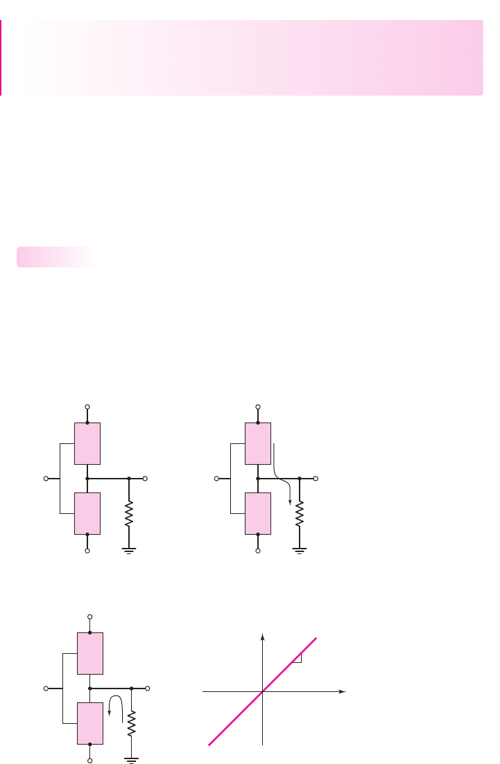
Idealized Class-B Operation
Figure 8.18(a) shows an idealized class-B output stage that consists of a comple-
mentary pair of electronic devices. When
v
I
= 0
, both devices are off, the bias
currents are zero, and
v
O
= 0
. For
v
I
> 0
, device A turns on and supplies current to
the load as shown in Figure 8.18(b). For
v
I
< 0
, device B turns on and sinks current
8.3.2
V
+
+
–
+
–
v
I
v
O
v
B
v
A
V
–
R
L
A
B
(a)
(c) (d)
V
+
v
I
< 0
v
O
< O
V
–
R
L
i
L
A
B
V
+
v
I
> 0 v
O
> 0
V
–
R
L
i
L
A
B
(b)
Slope = 1
v
O
v
I
Figure 8.18 (a) Idealized class-B output stage with complementary pair, A and B, of
electronic devices; (b) device A turns on for
v
I
> 0
, supplying current to the load; (c) device B
turns on for
v
I
< 0
, sinking current from the load; (d) ideal voltage transfer characteristics
nea80644_ch08_559-614.qxd 06/15/2009 01:31 PM Page 576 F506 Hard disk:Desktop Folder:ALI:MHDQ134-08 Folder:MHDQ134-08:
Chapter 8 Output Stages and Power Amplifiers 577
from the load as shown in Figure 8.18(c). Figure 8.18(d) shows the voltage transfer
characteristics. The ideal voltage gain is unity.
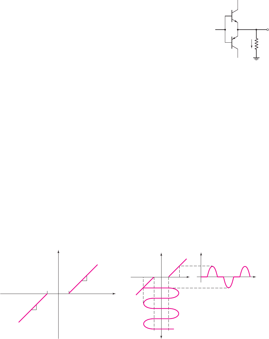
Approximate Class-B Circuit
Figure 8.19 shows an output stage that consists of a complementary pair of bipolar
transistors. When the input voltage is
v
I
= 0
, both transistors are cut off and the output
voltage is
v
O
= 0
. If we assume a B–E cut-in voltage of 0.6 V, then the output voltage
v
O
remains zero as long as the input voltage is in the range
−0.6 ≤ v
I
≤+0.6V
.
If
v
I
becomes positive and is greater than 0.6 V, then Q
n
turns on and operates as
an emitter follower. The load current i
L
is positive and is supplied through Q
n
, and the
B–E junction of Q
p
is reverse biased. If
v
I
becomes negative by more than 0.6 V, then
Q
p
turns on and operates as an emitter follower. Transistor Q
p
is a sink for the load
current, which means that i
L
is negative.
This circuit is called a complementary push–pull output stage. Transistor Q
n
conducts during the positive half of the input cycle, and Q
p
conducts during the
negative half-cycle. The transistors do not both conduct at the same time.
Figure 8.20 shows the voltage transfer characteristics for this circuit. When
either transistor is conducting, the voltage gain, which is the slope of the curve, is
essentially unity as a result of the emitter follower. Figure 8.21 shows the output
voltage for a sinusoidal input signal. When the output voltage is positive, the npn
transistor is conducting, and when the output voltage is negative, the pnp transistor is
conducting. We can see from this figure that each transistor actually conducts for
slightly less than half the time. Thus the bipolar push–pull circuit shown in Fig-
ure 8.19 is not exactly a class-B circuit.
We will see that an output stage using NMOS and PMOS transistors will
produce the same general voltage transfer characteristics.
Crossover Distortion
From Figure 8.20, we see that there is a range of input voltage around zero volts where
both transistors are cut off and
υ
O
is zero. This portion of the curve is called the dead
band. The output voltage for a sinusoidal input voltage is shown in Figure 8.21. The
output voltage is not a perfect sinusoidal signal, which means that crossover distortion
is produced by the dead band region.
V
–
V
+
Q
n
Q
p
v
O
v
I
R
L
i
L
Figure 8.19 Basic
complementary push–pull
output stage
v
O
v
I
0.6–0.6
Q
p
conducting
Q
n
cutoff
Q
n
conducting
Q
p
cutoff
Slope ≅ 1
Slope ≅ 1
Figure 8.20 Voltage transfer characteristics of basic
complementary push–pull output stage
v
O
v
O
t
v
I
t
Figure 8.21 Crossover distortion of basic
complementary push–pull output stage
nea80644_ch08_559-614.qxd 06/15/2009 01:31 PM Page 577 F506 Hard disk:Desktop Folder:ALI:MHDQ134-08 Folder:MHDQ134-08: