Neamen D. Microelectronics: Circuit Analysis and Design
Подождите немного. Документ загружается.

588 Part 1 Semiconductor Devices and Basic Applications
The maximum possible power conversion efficiency is then
η(max) =
¯
P
L
(max)
¯
P
S
=
1
2
·
V
2
CC
R
L
V
2
CC
R
L
=
1
2
⇒ 50%
(8.41)
This demonstrates that, in a standard class-A amplifier, replacing the collector resis-
tor with an inductor doubles the maximum possible power conversion efficiency.
Transformer-Coupled Common-Emitter Amplifier
The design of an inductively coupled amplifier to achieve high power conversion
efficiency may be difficult, depending on the relationship between the supply voltage
V
CC
and the load resistance R
L
. The effective load resistance can be optimized by
using a transformer with the proper turns ratio.
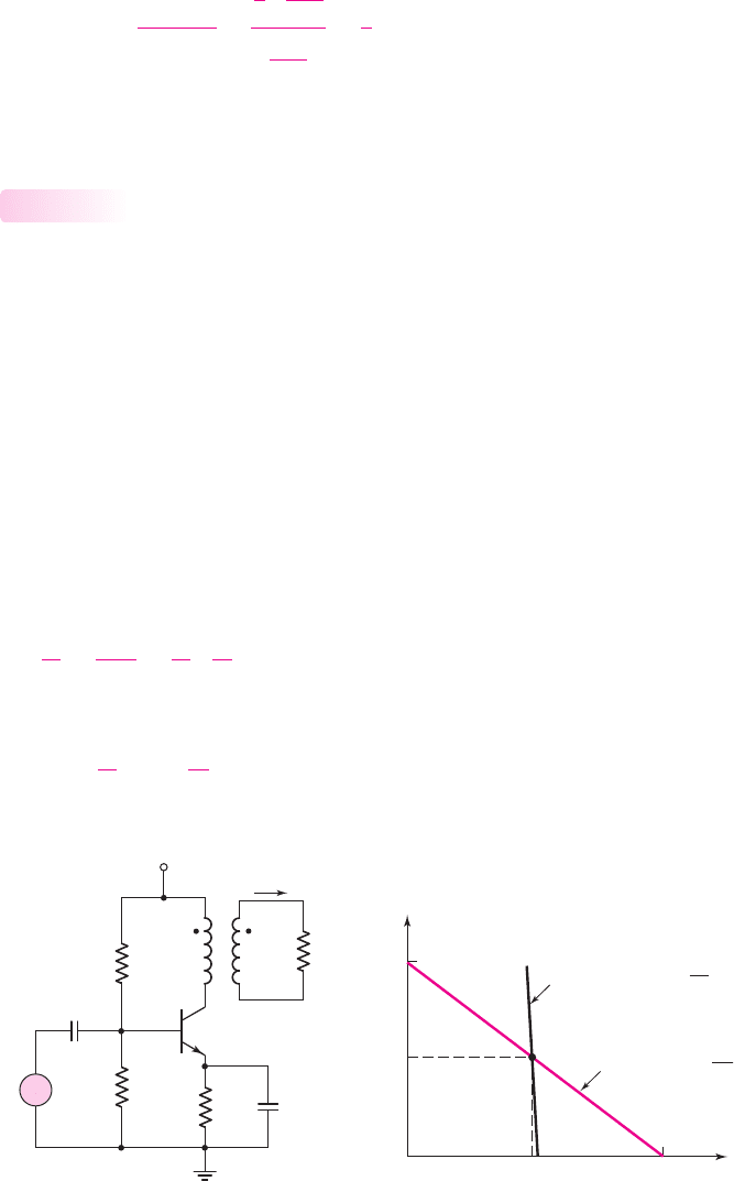
Figure 8.29(a) shows a common-emitter amplifier with a transformer-coupled
load in the collector circuit.
The dc and ac load lines are shown in Figure 8.29(b). If we neglect any resis-
tance in the transformer and assume that R
E
is small, the quiescent collector–emitter
voltage is
V
CEQ
∼
=
V
CC
Assuming an ideal transformer, the currents and voltages in Figure 8.29(a) are
related by
i
L
= ai
C
and
v
2
= v
1
/a
where a is the ratio of primary to secondary turns,
or simply the turns ratio. Dividing voltages by currents, we find
v
2
i
L
=
v
1
/a
ai
C
=
v
1
i
C
·
1
a
2
(8.42)
The load resistance is
R
L
= v
2
/i
L
. We can define a transformed load resistance as
R
L
=
v
1
i
C
= a
2
·
v
2
i
L
= a
2
R
L
(8.43)
8.4.2
(a)
(b)
v
CE
V
CC
I
CQ
i
C
2I
CQ
≈ 2V
CC
DC load line, slope = –
1
R
E
AC load line, slope = –
1
R
L
′
C
C
→ ∞
C
E
→ ∞
V
CC
R
2
R
E
R
1
R
L
a:1
+
–
v
2
+
–
v
1
v
i
+
–
i
L
Figure 8.29 (a) Transformer-coupled common-emitter amplifier and (b) dc and ac load lines
nea80644_ch08_559-614.qxd 06/15/2009 01:31 PM Page 588 F506 Hard disk:Desktop Folder:ALI:MHDQ134-08 Folder:MHDQ134-08:
Chapter 8 Output Stages and Power Amplifiers 589
The turns ratio is designed to produce the maximum symmetrical swing in the output
current and voltage; therefore,
R
L
=
2V
CC
2I
CQ
=
V
CC
I
CQ
= a
2
R
L
(8.44)
The maximum average power delivered to the load is equal to the maximum
average power delivered to the primary of the ideal transformer, as follows:
¯
P
L
(max) =
1
2
V
CC
I
CQ
(8.45)
where V
CC
and I
CQ
are the maximum possible amplitudes of the sinusoidal signals. If
we neglect the power dissipation in the bias resistors R
1
and R
2
, the average power
supplied by the V
CC
source is
¯
P
S
= V
CC
I
CQ
and the maximum possible power conversion efficiency is again
η(max) = 50%
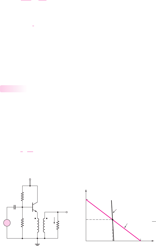
Transformer-Coupled Emitter-Follower Amplifier
Since the emitter follower has a low output impedance, it is often used as the output
stage of an amplifier.A transformer-coupledemitter follower is shownin Figure 8.30(a).
The dc and ac load lines are shown in Figure 8.30(b). As before, the resistance of the
transformer is assumed to be negligible.
The transformed load resistance is again
R
L
= a
2
R
L
. By correctly designing the
turns ratio, we can achieve the maximum symmetrical swing in the output voltage
and current.
The average power delivered to the load is
¯
P
L
=
1
2
·
V
2
p
R
L
(8.46)
8.4.3
v
CE
V
CC
I
CQ
i
C
2I
CQ
2V
CC
DC load line
AC load line, slope =
–
1
R
L
′
(a) (b)
C → ∞
v
i
v
o
V
CC
R
2
R
1
R
L
a:1
+
–
v
e
i
o
+
–
Figure 8.30 (a) Transformer-coupled emitter-follower amplifier and (b) dc and ac load lines
nea80644_ch08_559-614.qxd 06/15/2009 01:31 PM Page 589 F506 Hard disk:Desktop Folder:ALI:MHDQ134-08 Folder:MHDQ134-08:

590 Part 1 Semiconductor Devices and Basic Applications
where V
p
is the peak amplitude of the sinusoidal output voltage. The maximum peak
amplitude of the emitter voltage is V
CC
, so that the maximum peak amplitude of the
output signal is
V
p
(max) = V
CC
/a
The maximum average output signal power is therefore
¯
P
L
(max) =
1
2
·
[V
p
(max)]
2
R
L
=
V
2
CC
2a
2
R
L
(8.47)
The maximum power conversion efficiency for this circuit is also 50 percent.
DESIGN EXAMPLE 8.8
Objective: Design a transformer-coupled emitter-follower amplifier to deliver a
specified signal power.
Consider the circuit shown in Figure 8.30(a), with parameters
V
CC
= 24
V and
R
L
= 8
. The average power delivered to the load is to be 5 W, the peak amplitude
of the signal emitter current is to be no more than 0.9I
CQ
, and that of the signal emit-
ter voltage is to be no more than 0.9V
CC
. Let
β = 100
.
Solution: The average power delivered to the load is given by Equation (8.46). The
peak output voltage must therefore be
V
p
=
2R
L
¯
P
L
=
2(8)(5) = 8.94 V
and the peak output current is
I
p
=
V
p
R
L
=
8.94
8
= 1.12 A
Since
V
e
= 0.9 V
CC
= aV
p
then
a =
0.9 V
CC
V
p
=
(0.9)(24)
8.94
= 2.42
Also, since
I
e
= 0.9I
CQ
= I
p
/a
then
I
CQ
=
1
0.9
·
I
p
a
=
1.12
(0.9)(2.42)
= 0.514 A
The maximum power dissipated in the transistor, for this class-A operation, is
P
Q
= V
CC
I
CQ
= (24)(0.514) = 12.3W
so the transistor must be capable of handling this power.
Bias resistors R
1
and R
2
are found from a dc analysis. The Thevenin equivalent
voltage is
V
TH
= I
BQ
R
TH
+ V
BE
(on)
where
R
TH
= R
1
R
2
and V
TH
= [R
2
/(R
1
+ R
2
)] · V
CC
nea80644_ch08_559-614.qxd 06/15/2009 01:31 PM Page 590 F506 Hard disk:Desktop Folder:ALI:MHDQ134-08 Folder:MHDQ134-08:

Chapter 8 Output Stages and Power Amplifiers 591
We also have
I
BQ
=
I
CQ
β
=
0.514
100
⇒ 5.14 mA
Since
V
TH
< V
CC
and
I
BQ
∼
=
5mA
, then
R
TH
cannot be unduly large. How-
ever, if
R
TH
is small, then the power dissipation in R
1
and R
2
becomes unacceptably
high. We choose
R
TH
= 2.5
k, so that
V
TH
=
1
R
1
(R
TH
)V
CC
=
1
R
1
(2.5)(24) = (5.14)(2.5) + 0.7
Therefore,
R
1
= 4.43
k and R
2
= 5.74 k.
Comment: The average power delivered by V
CC
(neglecting bias resistor effects) is
¯
P
S
= V
CC
I
CQ
= 12.3W
, which means that the power conversion efficiency is
η = 5/12.3 ⇒ 40.7%
. The efficiency will always be less than the 50% maximum
value, if transistor saturation and distortion are to be minimized.
EXERCISE PROBLEM
*Ex 8.8: A transformer-coupled emitter-follower amplifier is shown in Fig-
ure 8.30(a). The parameters are:
V
CC
= 18
V,
V
BE
(on) = 0.7
V,
β = 100
,
a = 10
,
and
R
L
= 8
. (a) Design R
1
and R
2
to deliver the maximum power to the load.
The input resistance seen by the
v
i
source is to be 1.5 k. (b) If the peak ampli-
tude of the emitter voltage
v
E
is limited to 0.9V
CC
, and the peak amplitude of the
emitter current i
E
is limited to 0.9I
CQ
, determine the maximum amplitude of the
output signal voltage, and the average power delivered to the load. (Ans. (a) R
1
=
26.4 k, R
2
=
1.62 k (b) V
p
=
1.62 V, I
p
=
203 mA,
¯
P
L
= 0.164 W)
Test Your Understanding
*TYU 8.7 For the inductively coupled amplifier shown in Figure 8.28(a), the para-
meters are:
V
CC
= 12
V,
V
BE
(on) = 0.7
V,
R
E
= 0.1
k,
R
L
= 1.5
k, and
β = 75
.
(a) Design R
1
and R
2
for maximum symmetrical swing in the output current and volt-
age. (Let
R
TH
= (1 +β)R
E
.) (b) If the peak output voltage amplitude is limited to
0.9V
CC
, and the peak output current amplitude is limited to 0.9I
CQ
, determine the
average power delivered to the load, the average power dissipated in the transistor,
and the power conversion efficiency. (Ans. (a)
R
1
= 39.1
k,
R
2
= 9.43
k
(b)
¯
P
L
= 38.9mW
,
¯
P
Q
= 57.1mW
,
η = 40.5%
)
8.5 CLASS-AB PUSH–PULL COMPLEMENTARY
OUTPUT STAGES
Objective: • Analyze several circuit configurations of class-AB power
amplifiers.
A class-AB output stage eliminates the crossover distortion that occurs in a class-B
circuit. In this section, we will analyze several circuits that provide a small quiescent
bias to the output transistors. Such circuits are used as the output stage of power
nea80644_ch08_559-614.qxd 06/15/2009 01:31 PM Page 591 F506 Hard disk:Desktop Folder:ALI:MHDQ134-08 Folder:MHDQ134-08:
592 Part 1 Semiconductor Devices and Basic Applications
amplifiers, as well as the output stage of operational amplifiers, and will be discussed
in Chapter 13.
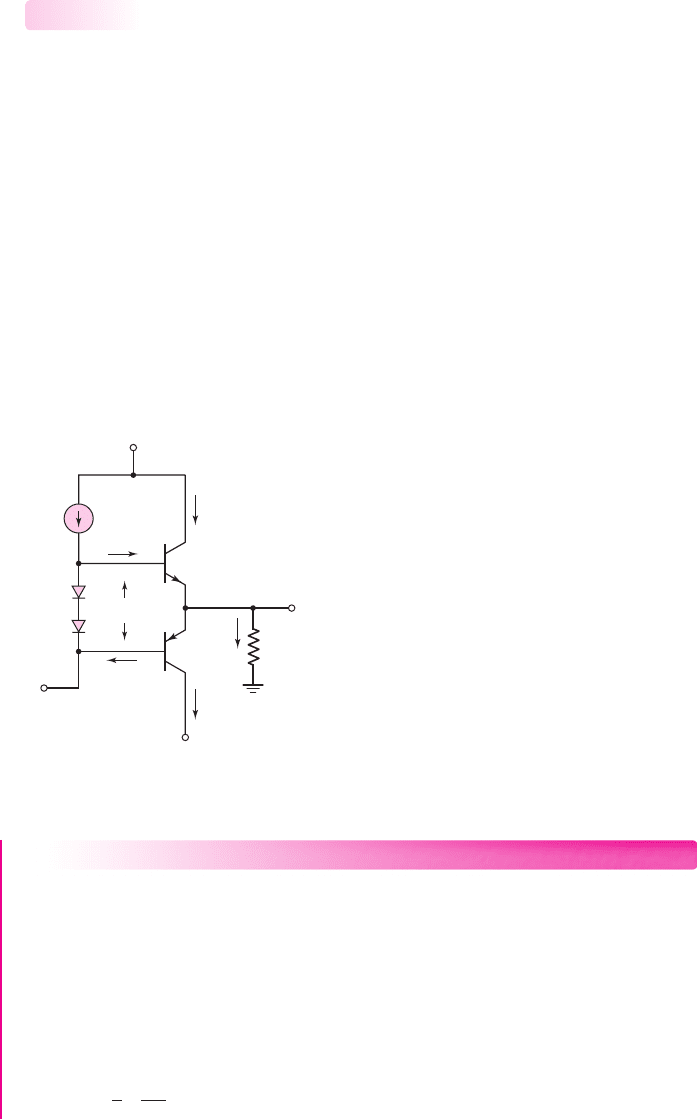
Class-AB Output Stage with Diode Biasing
In a class-AB circuit, the V
BB
voltage that provides the quiescent bias for the output
transistors can be established by voltage drops across diodes, as shown in Fig-
ure 8.31. A constant current I
Bias
is used to establish the required voltage across the
pair of diodes, or the diode-connected transistors, D
1
and D
2
. Since D
1
and D
2
are not
necessarily matched with Q
n
and Q
p
, the quiescent transistor currents may not be
equal to I
Bias
.
As the input voltage increases, the output voltage increases, causing an in-
crease in i
Cn
. This in turn produces an increase in the base current i
Bn
. Since the
increase in base current is supplied by I
Bias
, the current through D
1
and D
2
, and
hence the voltage V
BB
, decreases slightly. Since voltage V
BB
does not remain
constant in this circuit, the relationship between i
Cn
and i
Cp
, as given by Equa-
tion (8.35), is not precisely valid for this situation. The analysis in the previous sec-
tion must therefore be modified slightly, but the basic operation of this class-AB
circuit is the same.
8.5.1
V
+
V
–
i
Cn
i
Bn
I
Bias
D
1
D
2
Q
n
Q
p
R
L
i
Cp
i
Bp
i
L
v
O
v
I
+
–
V
BB
Figure 8.31 Class-AB output stage with quiescent bias established by diodes
DESIGN EXAMPLE 8.9
Objective: Design the class-AB output stage in Figure 8.31 to meet specific design
criteria.
Assume
I
SD
= 3 ×10
−14
A
for D
1
and D
2
,
I
SQ
= 10
−13
A for Q
n
and Q
p
, and
β
n
= β
p
= 75
. Let R
L
=
8 . The average power delivered to the load is to be 5 W.
The peak output voltage is to be no more than 80 percent of V
CC
, and the minimum
value of diode current I
D
is to be no less than 5 mA.
Solution: The average power delivered to the load, from Equation (8.24), is
¯
P
L
=
1
2
·
V
2
p
R
L
nea80644_ch08_559-614.qxd 06/15/2009 01:31 PM Page 592 F506 Hard disk:Desktop Folder:ALI:MHDQ134-08 Folder:MHDQ134-08:

Chapter 8 Output Stages and Power Amplifiers 593
Therefore,
V
p
=
2R
L
¯
P
L
=
2(8)(5) = 8.94 V
The supply voltages must then be
V
CC
=
V
p
0.8
=
8.94
0.8
= 11.2V
At this peak output voltage, the emitter current of Q
n
is approximately equal to the
load current, or
i
En
∼
=
i
L
(max) =
V
p
(max)
R
L
=
8.94
8
= 1.12 A
and the base current is
i
Bn
=
i
En
1 + β
n
=
1.12
76
⇒ 14.7mA
For a minimum
I
D
= 5
mA, we can choose
I
Bias
= 20
mA. For a zero input
signal, neglecting base currents, we find that
V
BB
= 2V
T
ln
I
D
I
SD
= 2(0.026) ln
20 × 10
−3
3 × 10
−14
= 1.416 V
The quiescent collector currents are then
I
CQ
= I
SQ
e
(V
BB
/2)V
T
= 10
−13
e
1.416/2(0.026)
⇒ 67.0mA
For
v
O
= 8.94
V and
i
L
= 1.12
A, the base current is
i
Bn
= 14.7
mA, and
I
D
= I
Bias
−i
Bn
= 5.3mA
The new value of V
BB
is then
V
BB
= 2V
T
ln
I
D
I
SD
= 2(0.026) ln
5.3 × 10
−3
3 × 10
−14
= 1.347 V
The B–E voltage of Q
n
is
v
BEn
= V
T
ln
i
Cn
I
SQ
= (0.026) ln
1.12
10
−13
= 0.781 V
The emitter–base voltage of Q
p
is then
v
EBp
= V
BB
−v
BEn
= 1.347 −0.781 = 0.566 V
and
i
Cp
= I
SQ
e
v
EBp
/V
T
= (10
−13
)e
0.566/0.026
⇒ 0.285 mA
Comment: When the output goes positive, the current in Q
p
decreases significantly,
as expected, but it does not go to zero. There is a factor of approximately 10
3
differ-
ence in the currents between Q
n
and Q
p
.
Design Pointer: If the output signal currents are large, the base currents in the
output transistors may become significant compared to the bias current through the
diodes D
1
and D
2
. The change in the diode bias current should be minimized in order
to keep the small-signal voltage gain of the output stage close to unity.
nea80644_ch08_559-614.qxd 06/15/2009 01:31 PM Page 593 F506 Hard disk:Desktop Folder:ALI:MHDQ134-08 Folder:MHDQ134-08:

594 Part 1 Semiconductor Devices and Basic Applications
EXERCISE PROBLEM
Ex 8.9: The BJT class-AB output stage shown in Figure 8.31 is biased at
V
+
= 5
V and
V
−
=−5
V. The load resistance is
R
L
= 1
k
. The device para-
meters are
I
SD
= 1.2 ×10
−14
A for the diodes and
I
SQ
= 2 ×10
−14
A for the
transistors. (a) Neglecting base currents, determine the value of
I
Bias
that induces
quiescent collector currents of
I
CQ
= 1
mA. (b) Assuming
β
n
= β
p
= 100
, deter-
mine
i
Cn
,
i
Cp
,
v
BEn
,
v
EBp
, and
I
D
for
v
O
= 1.2
V. (c) Repeat part (b) for
v
O
= 3 V
.
(Ans. (a)
I
Bias
= 0.6
mA; (b)
i
Cn
= 1.73
mA,
i
Cp
= 0.547
mA,
v
BEn
= 0.6547
V,
v
EBp
= 0.6248
V,
I
D
= 0.5827
mA; (c)
i
Cn
= 3.24
mA,
i
Cp
= 0.276
mA,
v
BEn
= 0.671
V,
v
EBp
= 0.607
V,
I
D
= 0.5676
mA)
Class-AB Biasing Using the V
BE
Multiplier
An alternative biasing scheme, which provides more flexibility in the design of the
output stage, is shown in Figure 8.32. The bias circuit that provides voltage V
BB
con-
sists of transistor Q
1
and resistors R
1
and R
2
, biased by a constant-current source I
Bias
.
If we neglect the base current in Q
1
, then
I
R
=
V
BE1
R
2
(8.48)
and voltage
V
BB
is
V
BB
= I
R
(R
1
+ R
2
) = V
BE1
1 +
R
1
R
2
(8.49)
Since voltage V
BB
is a multiplication of the junction voltage V
BE1
, the circuit is called
a V
BE
multiplier. The multiplication factor can be designed to yield the required
value of
V
BB
.
8.5.2
V
+
V
–
i
Cn
i
Bn
I
Bias
Q
n
Q
p
R
L
R
1
R
2
i
Cp
I
C1
i
Bp
i
L
I
R
v
O
v
I
+
–
V
BB
Q
1
Figure 8.32 Class-AB output stage with V
BE
multiplier bias circuit
nea80644_ch08_559-614.qxd 06/15/2009 01:31 PM Page 594 F506 Hard disk:Desktop Folder:ALI:MHDQ134-08 Folder:MHDQ134-08:
Chapter 8 Output Stages and Power Amplifiers 595
A fraction of the constant current I
Bias
flows through Q
1
, so that
V
BE1
= V
T
ln
I
C1
I
S1
(8.50)
Also, the quiescent bias currents i
Cn
and i
Cp
are normally small; therefore, we can
neglect
i
Bn
and
i
Bp
. Current
I
Bias
divides between I
R
and I
C1
, satisfying both Equa-
tions (8.48) and (8 50).
As
v
I
increases,
v
O
becomes positive, and
i
Cn
and
i
Bn
increase, which reduces
the collector current in Q
1
. However, the logarithmic dependence of I
C1
, shown in
Equation (8.50), means that
V
BE1
and, in turn
V
BB
remain essentially constant as the
output voltage changes.
DESIGN EXAMPLE 8.10
Objective: Design a Class-AB output stage using the
V
BE
multiplier circuit to meet
a specified total harmonic distortion.
Assume the circuit in Figure 8.32, biased at
V
+
= 15
V and
V
−
=−15 V
, is the
output stage of an audio amplifier that is to drive another power amplifier whose
input resistance is 1 k. The maximum peak sinusoidal output voltage is to be 10 V
and the total harmonic distortion is to be less than 0.1 percent.
Solution: Standard 2N3904 and 2N3906 transistors are to be used. From the results
of Example 8.6, the THD is a function of the output transistor quiescent currents. For
the basic circuit in Figure 8.24, the THD is found to be 0.097 percent for
V
BB
=
1.346
V, quiescent collector currents of 0.88 mA, and a peak sinusoidal output volt-
age of 10 V.
Figure 8.33 is the PSpice circuit schematic. For a peak output voltage of 10 V,
the peak load current is 10 mA. Assuming
β
∼
=
100
, the peak base current is 0.1 mA.
+
–
2N3904
V
2N3904
2N3906
0
2N3906
0
3.48 kΩ
0
+
–
15 V
I
1
1 mA
I
DC
Q
1
Q
3
V
1
0
+
–
–15 V
V
2
V
ou
t
Q
2
Q
4
V
3
R
1
1 k
R
3
3.25 kΩ
R
2
Figure 8.33 PSpice circuit schematic for Example 8.10
nea80644_ch08_559-614.qxd 06/15/2009 01:31 PM Page 595 F506 Hard disk:Desktop Folder:ALI:MHDQ134-08 Folder:MHDQ134-08:

596 Part 1 Semiconductor Devices and Basic Applications
A bias current of 1 mA is chosen to bias the
V
BE
multiplier. The peak 0.1 mA
base current, then, will not greatly disturb the current through the multiplier
circuit.
We may select
I
R
= 0.2
mA (current through R
1
and R
2
) and
I
C3
= 0.8
mA. We
then have
R
1
+ R
2
=
V
BB
I
R
=
1.346
0.2
= 6.73 k
For the 2N3904, we find that
V
BE
∼
=
0.65 V
for a quiescent collector current of
approximately 0.8 mA. Therefore
R
2
=
V
BE3
I
R
=
0.65
0.2
= 3.25 k
so that
R
1
= 3.48
k.
From the PSpice results, we find that the voltage at the base of Q
1
to be
0.6895 V and the voltage at the base of Q
2
to be
−0.6961 V
, which means that
V
BB
=
1.3856
V. This voltage is slightly greater than the design value of
V
BB
= 1.346
V.
Listed below are the quiescent transistor parameters. The quiescent collector
currents of the output transistors are 1.88 mA, approximately twice the design value
of 0.88 mA. The total harmonic distortion is 0.0356 percent, which is well within
the design specification.
NAME Q_Q1 Q_Q2 Q_Q3 Q_Q4
MODEL Q2N3904 Q2N3906 Q2N3904 Q2N3906
IB 1.12E-05 -5.96E-06 6.01E-06 -3.20E-06
IC 1.88E-03 -1.88E-03 7.80E-04 -9.92E-04
VBE 6.78E-01 -7.08E-01 6.59E-01 -6.92E-01
VBC -1.43E+01 1.43E+01 -7.27E-01 1.36E+01
VCE 1.50E+01 -1.50E+01 1.39E+00 -1.43E+01
BETADC 1.67E+02 3.15E+02 1.30E+02 3.10E+02
GM 7.11E-02 7.15E-02 2.98E-02 3.80E-02
RPI 2.66E+03 4.34E+03 5.01E+03 8.09E+03
Comment: Since the resulting
V
BB
voltage is slightly larger than the design value,
the quiescent output transistor currents are approximately double the design value.
Although the THD specification is met, the larger collector currents mean a larger
quiescent power dissipation. For this reason, the circuit may need to be redesigned
slightly to lower the quiescent currents.
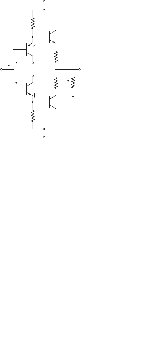
Class-AB Output Stage with Input
Buffer Transistors
The output stage in Figure 8.34 is a class-AB configuration composed of the com-
plementary transistor pair Q
3
and Q
4
. Resistors R
1
and R
2
and the emitter-follower
transistors Q
1
and Q
2
establish the quiescent bias required in this configuration.
Resistors R
3
and R
4
, used in conjunction with short-circuit protection devices not
shown in the figure, also provide thermal stability for the output transistors. The
input signal
v
I
may be the output of a low-power amplifier. Also, since this is an
emitter follower, the output voltage is approximately equal to the input voltage.
8.5.3
nea80644_ch08_559-614.qxd 06/15/2009 01:31 PM Page 596 F506 Hard disk:Desktop Folder:ALI:MHDQ134-08 Folder:MHDQ134-08:
Chapter 8 Output Stages and Power Amplifiers 597
When the input voltage
v
I
increases from zero, the base voltage of Q
3
increases,
and the output voltage
v
O
increases. The load current i
O
is positive, and the emitter
current in Q
3
increases to supply the load current, which causes an increase in the
base current into Q
3
. Since the base voltage of Q
3
increases, the voltage drop across
R
1
decreases, resulting in a smaller current in R
1
. This means that i
E1
and i
B1
also
decrease. As
v
I
increases, the voltage across R
2
increases, and i
E2
and i
B2
increase. A
net input current i
I
is then produced, to account for the reduction in i
B1
and the
increase in i
B2
.
The net input current is
i
I
= i
B2
−i
B1
(8.51)
Neglecting the voltage drops across R
3
and R
4
and the base currents in Q
3
and Q
4
,we
have
i
B2
=
(v
I
− V
BE
) − V
−
(1 + β
n
)R
2
(8.52(a))
and
i
B1
=
V
+
−(v
I
+ V
EB
)
(1 + β
p
)R
1
(8.52(b))
where β
n
and β
p
are the current gains of the npn and pnp transistors, respectively. If
V
+
=−V
−
,
V
BE
= V
EB
,
R
1
= R
2
≡ R
, and
β
n
= β
p
≡ β
, then combining Equa-
tions (8.52(a)), (8.52(b)), and (8.51) produces
i
I
=
(v
I
− V
BE
− V
−
)
(1 + β)R
−
(V
+
−v
I
− V
EB
)
(1 + β)R
=
2v
I
(1 + β)R
(8.53)
V
+
V
+
V
–
V
–
i
B1
i
B2
Q
3
Q
4
R
L
R
3
R
4
R
1
R
2
i
I
i
O
v
O
v
I
i
E1
i
E2
Q
1
Q
2
Figure 8.34 Class-AB output stage with input buffer transistors
nea80644_ch08_559-614.qxd 06/15/2009 01:31 PM Page 597 F506 Hard disk:Desktop Folder:ALI:MHDQ134-08 Folder:MHDQ134-08: