Neamen D. Microelectronics: Circuit Analysis and Design
Подождите немного. Документ загружается.


598 Part 1 Semiconductor Devices and Basic Applications
Since the voltage gain of this output stage is approximately unity, the output current is
i
O
=
v
O
R
L
∼
=
v
I
R
L
(8.54)
Using Equations (8.53) and (8.54), we find the current gain of this output stage to be
A
i
=
i
O
i
I
=
(1 + β)R
2R
L
(8.55)
With
β
in the numerator, this current gain should be substantial. A large current gain
is desirable, since the output stage of power amplifiers must provide the current
necessary to meet the power requirements.
EXAMPLE 8.11
Objective: Determine the currents and the current gain for the output stage with
input buffer transistors.
For the circuit in Figure 8.34, the parameters are:
R
1
= R
2
= 2
k,
R
L
= 100
,
R
3
= R
4
= 0
, and
V
+
=−V
−
= 15 V
. Assume all transistors are matched, with
β = 60
and
V
BE
(npn) = V
EB
(pnp) = 0.6
V.
Solution: For
v
I
= 0
,
i
R1
= i
R2
∼
=
i
E1
= i
E2
=
15 − 0.6
2
= 7.2mA
Assuming all transistors are matched, the bias currents in Q
3
and Q
4
are also approx-
imately 7.2 mA, since the base–emitter voltages of Q
1
and Q
3
are equal and those of
Q
2
and Q
4
are equal.
Solution: For
v
I
= 10
V, the output current is approximately
i
O
=
v
O
R
L
∼
=
10
0.1
= 100 mA
The emitter current in Q
3
is essentially equal to the load current, which means that
the base current in Q
3
is approximately
i
B3
= 100/61 = 1.64 mA
The current in R
1
is
i
R1
=
15 − (10 +0.6)
2
= 2.2mA
which means that
i
E1
= i
R1
−i
B3
= 0.56 mA
and
i
B1
= i
E1
/(1 + β) = 0.56/61 ⇒ 9.18 μA
Since Q
4
tends to turn off when
v
O
increases, we have
i
E2
∼
=
i
R2
=
10 − 0.6 −(−15)
2
= 12.2mA
nea80644_ch08_559-614.qxd 06/15/2009 01:31 PM Page 598 F506 Hard disk:Desktop Folder:ALI:MHDQ134-08 Folder:MHDQ134-08:

Chapter 8 Output Stages and Power Amplifiers 599
and
i
B2
= i
E2
/(1 + β) = 12.2/61 ⇒ 200 μA
The input current is then
i
I
= i
B2
−i
B1
= 200 −9.18
∼
=
191 μA
The current gain is then
A
i
=
i
O
i
I
=
100
0.191
= 524
From Equation (8.55), the predicted current gain is
A
i
=
i
O
i
I
=
(1 + β)R
2R
L
=
(61)(2)
2(0.1)
= 610
Comment: Since the current gain determined from Equation (8.55) neglects
base currents in Q
3
and Q
4
, the actual current gain is less than the predicted value, as
expected. The input current of 191 μA can easily be supplied by a low-power
amplifier.
EXERCISE PROBLEM
Ex 8.11: Consider the class-AB output stage in Figure 8.34. The parameters are:
V
+
=−V
−
= 12 V
,
R
1
= R
2
= 250
,
R
L
= 8
, and
R
3
= R
4
= 0
. Assume
all transistors are matched, with
β = 40
and
V
BE
(npn) = V
EB
(pnp) = 0.7
V.
(a) For
v
I
= 0
, determine i
E1
, i
E2
, i
B1
, and i
B2
. (b) For
v
I
= 5
V, find i
O
, i
E1
, i
E2
, i
B1
,
i
B2
, and i
I
. (c) Using the results of part (b), determine the current gain of the output
stage. Compare this value to that found using Equation (8.55). (Ans. (a)
i
E1
=
i
E2
= 44.1
mA,
i
B1
= i
B2
= 1.08
mA (b)
i
O
= 0.625
A,
i
E1
= 10.0
mA,
i
B1
= 0.244
mA,
i
E2
= 65.2
mA,
i
B2
= 1.59
mA,
i
I
= 1.35
mA (c)
A
i
= 463
,
from Equation (8.55) A
i
= 641)
Class-AB Output Stage Utilizing
the Darlington Configuration
The complementary push–pull output stage uses npn and pnp bipolar transistors.
Usually in IC design, the pnp transistors are fabricated as lateral devices with low β
values that are typically in the range of 5 to 10, and the npn transistors are fabricated
as vertical devices with β values on the order of 200. This means that the npn and pnp
transistors are not well matched, as we have assumed in our analyses.
Consider the two-transistor configuration shown in Figure 8.35(a). Assume the
transistor current gains are β
n
and β
p
for the npn and pnp transistors, respectively. We
can write
i
Cp
= i
Bn
= β
p
i
Bp
(8.56)
and
i
2
= (1 +β
n
)i
Bn
= (1 +β
n
)β
p
i
Bp
∼
=
β
n
β
p
i
Bp
(8.57)
8.5.4
nea80644_ch08_559-614.qxd 06/15/2009 01:31 PM Page 599 F506 Hard disk:Desktop Folder:ALI:MHDQ134-08 Folder:MHDQ134-08:
600 Part 1 Semiconductor Devices and Basic Applications
Terminal 1 acts as the base of the composite three-terminal device, terminal 2 acts as
the collector, and terminal 3 is the emitter. The current gain of the device is then
approximately β
n
β
p
. The equivalent circuit is shown in Figure 8.35(b). We can use
the two-transistor configuration in Figure 8.35(a) as a single equivalent pnp transistor
with a current gain on the same order of magnitude as that of an npn device.
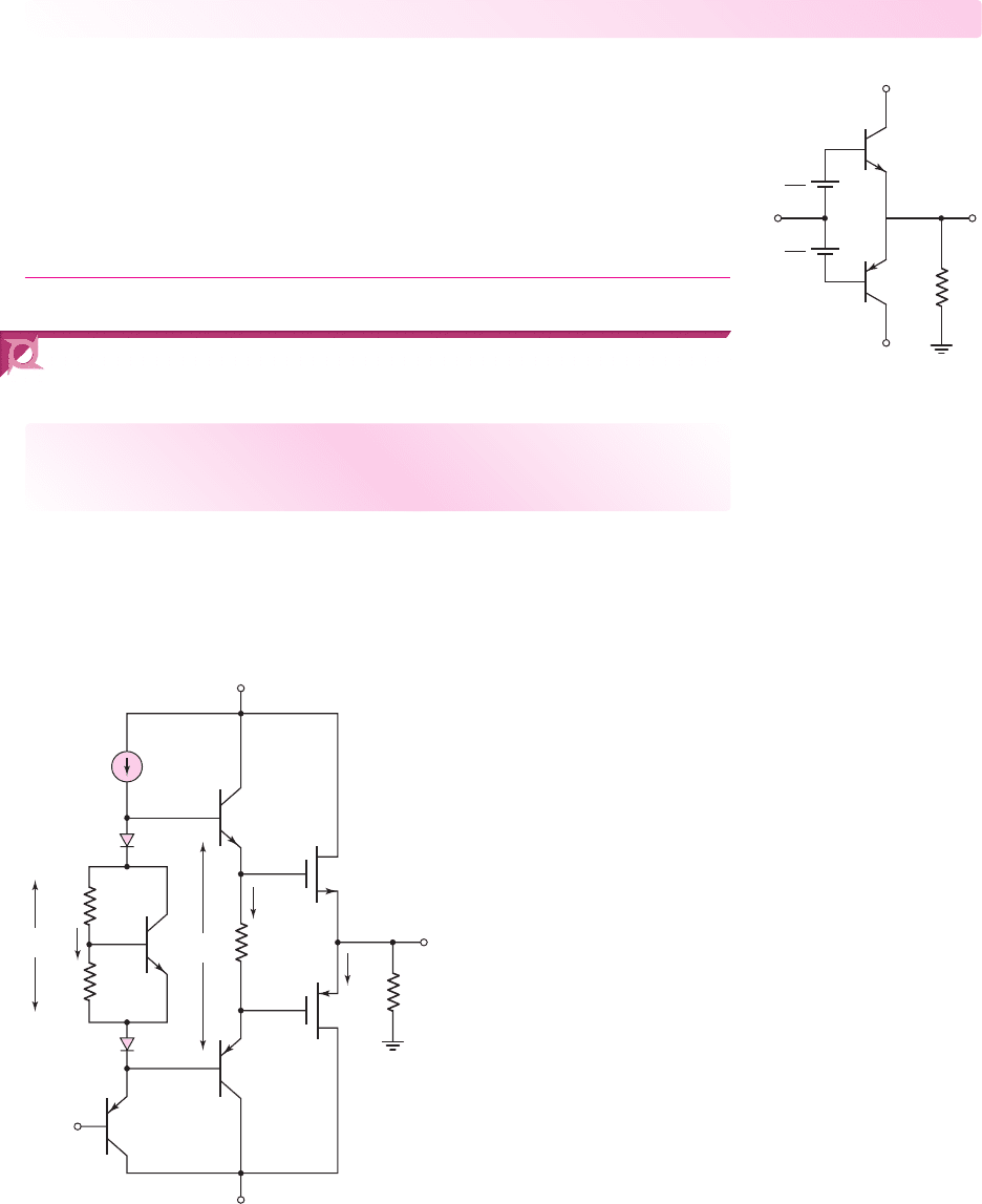
In Figure 8.36, the output stage uses Darlington pairs to provide the necessary
current gain. Transistors Q
1
and Q
2
constitute the npn Darlington emitter-follower
that sources current to the load. Transistors Q
3
, Q
4
, and Q
5
constitute a composite pnp
Darlington emitter follower that sinks current from the load. The three diodes D
1
, D
2
,
and D
3
establish the quiescent bias for the output transistors.
The effective current gain of the three-transistor configuration Q
3
–Q
4
–Q
5
is
essentially the product of the three individual gains. With the low current gain of the
pnp device Q
3
, the overall current gain of the Q
3
–Q
4
–Q
5
configuration is similar to
that of the Q
1
–Q
2
pair.
V
+
V
+
V
–
V
–
I
Bias
D
2
D
3
Q
1
R
L
i
O
v
O
v
I
D
1
Q
6
Q
3
Q
4
Q
5
+
–
V
BB
Q
2
Figure 8.36 Class-AB output stage with Darlington pairs
i
Cp
= i
Bn
i
Cn
i
Bp
i
1
i
Ep
i
2
1
3
2
Q
p
Q
n
(a) (b)
i
B
i
C
i
E
1
3
2
B
E
C
b
≅ b
n
b
p
Figure 8.35 (a) A two-transistor configuration of an equivalent pnp transistor; (b) the
equivalent pnp transistor
nea80644_ch08_559-614.qxd 06/15/2009 01:31 PM Page 600 F506 Hard disk:Desktop Folder:ALI:MHDQ134-08 Folder:MHDQ134-08:
Chapter 8 Output Stages and Power Amplifiers 601
Test Your Understanding
TYU 8.8 Consider the class-AB output stage shown in Figure 8.37. The transistor pa-
rameters are
β
n
= 100
and
I
Sn
= 5 ×10
−16
A for the npn device, and
β
p
= 100
and
I
Sp
= 8 ×10
−16
A for the pnp device. (a) What value of
V
BB
will establish quiescent
collector currents of
I
CQ
= 1
mA with
v
O
= 0
. (b) What are the values of
v
BEn
and
v
EBp
? (c) What must be the value of
v
I
such that
v
O
= 0
. (Ans. (a)
V
BB
= 1.4606
V;
(b)
v
BEn
= 0.7364
V,
v
EBp
= 0.7242
V; (c)
v
I
= 6.1
mV)
TYU 8.9 From Figure 8.36, show that the overall current gain of the three-transistor
configuration composed of Q
3
, Q
4
, and Q
5
is approximately
β = β
3
β
4
β
5
.
8.6 DESIGN APPLICATION: AN OUTPUT STAGE
USING MOSFET
S
Objective: • Design an output stage using power MOSFETs as the
output devices.
Specifications: The output stage configuration to be designed is shown in Fig-
ure 8.38. The current I
Bias
is 5 mA and the zero output quiescent current in M
n
and M
p
is to be 0.5 mA.
I
Bias
Q
1
V
+
= 10 V
V
–
= –10 V
Q
4
Q
2
R
2
I
2
Q
3
V
D
M
P
M
N
R
L
v
O
v
I
R
A
I
R
V
M
V
BB
R
B
+
–
V
D
+
+
–
+
–
–
I
NP
Figure 8.38 Output stage for design application
Q
n
Q
p
v
I
R
L
V
BB
2
V
BB
2
V
–
= –3 V
–
–
+
+
V
+
= 3 V
v
O
Figure 8.37 Figure for
exercise TYU 8.8
nea80644_ch08_559-614.qxd 06/15/2009 01:31 PM Page 601 F506 Hard disk:Desktop Folder:ALI:MHDQ134-08 Folder:MHDQ134-08:

602 Part 1 Semiconductor Devices and Basic Applications
Design Pointer: The output devices are to be MOSFETs because of their superior
power characteristics. The low output resistance of the emitter follower transistors
Q
1
and Q
2
tends to increase switching speed of the output transistors. The voltage
drop across resistor R
2
provides the bias to M
n
and M
p
so that crossover distortion is
minimized.
Choices: MOSFETs with parameters
V
TN
= 0.8
V,
V
TP
=−0.8V
,
K
n
= K
p
=
5 mA/V
2
, and
λ = 0
are available. BJTs with parameters
I
S1
= I
S2
= 10
−12
A
,
I
S3
= I
S4
= 2 ×10
−13
A
, and
β = 150
are available. Also diodes with parameters
I
SD
= 5 ×10
−13
A
are available.
Solution: For
I
NP
= 0.5
mA, the gate-to-source voltages are found from
I
NP
= K
n
(V
GSn
− V
TN
)
2
or
0.5 = 5(V
GSn
−0.8)
2
Since the two output transistors are matched, we have
V
GSn
= V
SGp
= 1.116 V
If we design for I
2
= 2 mA, then the value of resistor R
2
is
R
2
=
2(1.116)
2
= 1.116 k
Considering the BJTs, we find
V
BE1
= V
EB2
= V
T
ln
I
2
I
S1
= (0.026) ln
2 × 10
−3
10
−12
= 0.5568 V
We then have
V
BB
= 2(0.5568) + 2(1.116) = 3.3456 V
Neglecting base currents, the voltages across the diodes are
V
D
= V
T
ln
I
D
I
SD
= (0.026) ln
5 × 10
−3
5 × 10
−13
= 0.5987 V
The voltage across the
V
BE
multiplier circuit is found to be
V
M
= V
BB
−2V
D
= 3.3456 −2(0.5987) = 2.1482 V
We will design the
V
BE
multiplier circuit such that
I
C3
= (0.9)I
Bias
and
I
R
=
(0.1)I
Bias
. Then
V
BE3
= V
T
ln
I
C3
I
S3
= (0.026) ln
(0.9)(5 × 10
−3
)
2 × 10
−13
or
V
BE3
= 0.6198 V
We also have
R
B
=
V
BE3
I
R
=
0.6198
(0.1)(5 × 10
−3
)
= 1.24 k
nea80644_ch08_559-614.qxd 06/15/2009 01:31 PM Page 602 F506 Hard disk:Desktop Folder:ALI:MHDQ134-08 Folder:MHDQ134-08:

Chapter 8 Output Stages and Power Amplifiers 603
From Equation (8.48), we have
V
M
= V
BE3
1 +
R
A
R
B
or
2.1482 = (0.6198)
1 +
R
A
R
B
which yields
R
A
/R
B
= 2.466
, so that
R
A
= 2.466 R
B
= 3.06
k.
We see that
V
EB4
= V
T
ln
I
Bias
I
C4
= (0.026) ln
5 × 10
−3
2 × 10
−13
= 0.6225 V
Then, for
v
O
= 0
, the input voltage
v
I
must be
v
I
=−V
SGP
− V
EB2
− V
EB4
=−1.116 − 0.5568 −0.6225
or
v
I
=−2.295 V
Comment: The required input voltage
v
I
to yield
v
O
= 0
would be designed from
the previous stage of the amplifier. In addition, the circuit required to establish the
I
Bias
current will be considered in Chapter 10. We may notice that, except for
I
Bias
,
all the design parameters are independent of the bias voltages
V
+
and
V
−
.
8.7 SUMMARY
• In this chapter, we analyzed and designed amplifiers and output stages capable
of delivering a substantial amount of power to a load.
• The current, voltage, and power ratings of BJTs and MOSFETs were consid-
ered, and the safe operating area for the transistors was defined in terms of these
limiting parameters. The maximum power rating of a transistor is related to the
maximum allowed device temperature at which the device can operate without
being damaged.
• Several classes of power amplifiers were defined.
• In a class-A amplifier, the output transistor conducts 100 percent of the time.
The theoretical maximum power efficiency for a standard class-A amplifier is 25
percent. This efficiency can be theoretically increased to 50 percent by incorpo-
rating inductors and transformers in the circuit.
• Class-B output stages are composed of complementary pairs of transistors oper-
ating in a push-pull manner. In an ideal class-B operation, each output transistor
conducts 50 percent of the time. For an idealized class-B output stage, the theo-
retical maximum power conversion efficiency is 78.5 percent. However, practi-
cal class-B output stages tend to suffer from crossover distortion effects when
the output is in the vicinity of zero volts.
• The class-AB output stage is similar to the class-B circuit, except that each out-
put transistor is provided with a small quiescent bias and conducts slightly more
than 50 percent of the time. The power conversion efficiency of this circuit is less
than that of a class-B circuit, but is substantially larger than that of the class-A
circuit. In addition, the crossover distortion is greatly reduced.
• As an application, a class-AB output stage using MOSFETs was designed.
nea80644_ch08_559-614.qxd 06/15/2009 01:31 PM Page 603 F506 Hard disk:Desktop Folder:ALI:MHDQ134-08 Folder:MHDQ134-08:

604 Part 1 Semiconductor Devices and Basic Applications
CHECKPOINT
After studying this chapter, the reader should have the ability to:
✓ Describe what factors are related to the maximum transistor current and
maximum transistor voltage.
✓ Define the safe operating area of a transistor and define the power derating
curve.
✓ Define the power conversion efficiency of an output stage.
✓ Describe the operation of a class-A output stage.
✓ Describe the operation of an ideal class-B output stage and discuss the concept
of crossover distortion.
✓ Describe and design a class-AB output stage and discuss why crossover distor-
tion is essentially eliminated.
REVIEW QUESTIONS
1. Discuss the limiting factors for the maximum rated current and maximum rated
voltage in a BJT and MOSFET.
2. Describe the safe operating area for a transistor.
3. Why is an interdigitated structure typically used in a high-power BJT design?
4. Discuss the role of thermal resistance between various junctions in a high-power
transistor structure.
5. Define and describe the power derating curve for a transistor.
6. Define power conversion efficiency for an output stage.
7. Describe the operation of a class-A output stage.
8. Describe the operation of an ideal class-B output stage.
9. Discuss crossover distortion.
10. What is meant by harmonic distortion?
11. Describe the operation of a class-AB output stage and why a class-AB output
stage is important.
12. Describe the operation of a transformer-coupled class-A common-emitter
amplifier.
13. Sketch a class-AB complementary BJT push–pull output stage using a V
BE
multiplier circuit.
14. Sketch a class-AB complementary MOSFET push-pull output stage using all
MOSFETs.
15. What are the advantages of a Darlington pair configuration?
16. Sketch a two-transistor configuration using npn and pnp BJTs that are equivalent
to a single pnp BJT.
PROBLEMS
Section 8.2 Power Transistors
8.1 The maximum current, voltage, and power ratings of a power MOSFET are
4 A, 40 V, and 30 W, respectively. (a) Sketch and label the safe operating area
for this transistor, using linear current and voltage scales. (b) For the com-
mon-source circuit shown in Figure P8.1, determine
R
D
and sketch the load
nea80644_ch08_559-614.qxd 06/15/2009 01:31 PM Page 604 F506 Hard disk:Desktop Folder:ALI:MHDQ134-08 Folder:MHDQ134-08:

Chapter 8 Output Stages and Power Amplifiers 605
line that produces a maximum power in the transistor for (i)
V
DD
= 24
V and
(ii)
V
DD
= 40
V. (c) Using the results of part (b), determine the maximum
possible drain current for (i)
V
DD
= 24
V and (ii)
V
DD
= 40
V.
8.2 The common-emitter circuit in Figure P8.2 is biased at
V
CC
= 24
V. The
maximum transistor power is rated at
P
Q,max
= 25
W. The other parame-
ters of the transistor are
β = 60
and
V
BE
(
on
)
= 0.7
V. (a) Determine
R
L
and
R
B
such that the transistor is biased at the maximum power
point. (b) For
V
p
= 12
mV, determine the average power dissipated in the
transistor.
8.3 For the transistor in the common-emitter circuit in Figure P8.2, the parame-
ters are:
β = 80
,
P
D,max
= 10
W,
V
CE
(
sus
)
= 30
V, and
I
C,max
= 1.2
A.
(a) Design the values of
R
L
and
R
B
for
V
CC
= 30
V. What is maximum
power dissipated in the transistor? (b) Using the value of
R
L
in part (a), find
I
C,max
and
V
CC
if
P
D,max
= 5
W. (c) Calculate the maximum undistorted ac
power that can be delivered to
R
L
in parts (a) and (b) for the assumption that
i
C
≥ 0
and
0 ≤ v
CE
≤ V
CC
.
8.4 Sketch the safe operating region for a MOSFET. Label three arbitrary points
on the maximum hyperbola. Assume each of the labeled points is a Q-point
and draw a tangent load line through each point. Discuss the advantages
or disadvantages of each point relative to the maximum possible signal
amplitude.
8.5 A power MOSFET is connected in a common-source configuration as
shown in Figure P8.1. The parameters are: I
D,max
=
4 A, V
DS,max
=
50 V,
P
D,max
=
35 W, V
TN
=
4 V, and K
n
=
0.25 A/V
2
. The circuit parameters are
V
DD
=
40 V and R
L
=
10 . (a) Sketch and label the safe operating area for
this transistor, using linear current and voltage scales. Also sketch the load
line on the same graph. (b) Calculate the power dissipated in the transistor
for V
GG
=
5, 6, 7, 8, and 9 V. (c) Is there a possibility of damaging the
transistor? Explain.
D8.6 Consider the common-source circuit shown in Figure P8.6. The transistor
parameters are V
TN
=
4 V and K
n
=
0.2 A/V
2
. (a) Design the bias circuit
such that the Q-point is in the center of the load line. (b) What is the power
dissipated in the transistor at the Q-point? (c) Determine the minimum rated
I
D,max
, V
DS,max
, and P
D,max
values. (d) If
v
i
= 0.5 sin ωt V
, calculate the ac
R
B
R
L
C
v
S
= V
p
sin
w
t
(V)
V
CC
+
–
Figure P8.2
V
DD
V
GG
R
D
Figure P8.1
nea80644_ch08_559-614.qxd 06/15/2009 01:31 PM Page 605 F506 Hard disk:Desktop Folder:ALI:MHDQ134-08 Folder:MHDQ134-08:

606 Part 1 Semiconductor Devices and Basic Applications
power delivered to R
L
, and determine the average power dissipated in the
transistor.
R
2
C → ∞
v
i
R
1
R
L
= 20 Ω
V
DD
= 50 V
v
O
+
–
Figure P8.6
8.7 A particular transistor is rated for a maximum power dissipation of 60 W if
the case temperature is at 25 °C. Above 25 °C, the allowed power dissipa-
tion is reduced by 0.5W/°C. (a) Sketch the power derating curve. (b) What
is the maximum allowed junction temperature? (c) What is the value of
θ
dev−case
?
8.8 A MOSFET has a rated power of 50 W and a maximum specified junction
temperature of 150 °C. The ambient is T
amb
=
25 °C. Find the relationship
between the actual operating power and
θ
case−amb
.
8.9 For a power MOSFET,
θ
dev−case
= 1.5
◦
C/W,
θ
snk−amb
= 2.8
◦
C/W, and
θ
case−snk
= 0.6
◦
C/W. The ambient temperature is
25
◦
C
. (a) If the maximum
junction temperature is limited to
T
j,max
= 120
◦
C, determine the maximum
allowed power dissipation. (b) Using the results of part (a), determine the
temperature of the case and heat sink.
8.10 A power BJT must dissipate 30 W of power. The maximum allowed junc-
tion temperature is
T
j,max
= 150
◦
C, the ambient temperature is
25
◦
C, and
the device-to-case thermal resistance is
θ
dev−case
= 2.8
◦
C/W. (a) Find the
maximum permissible thermal resistance between the case and ambient.
(b) Using the results of part (a), determine the junction temperature if the
power dissipated in the transistor is 20 W.
8.11 The quiescent collector current in a BJT is
I
CQ
= 3
A. The maximum al-
lowed junction temperature is
T
j,max
= 150
◦
C and the ambient temperature
is
T
amb
= 25
◦
C. Other parameters are
θ
snk−amb
= 3.8
◦
C/W,
θ
case−snk
=
1.5
◦
C/W, and
θ
dev−case
= 4
◦
C/W. (a) Determine the power that can be
safely dissipated in the transistor. (b) Using the results of part (a), determine
the maximum collector-emitter voltage that may be applied.
Section 8.3 Classes of Amplifiers
8.12 For the class-A amplifier shown in Figure 8.16(a), show that the maximum
theoretical conversion efficiency for a symmetrical square-wave input
signal is 50 percent.
nea80644_ch08_559-614.qxd 06/15/2009 01:31 PM Page 606 F506 Hard disk:Desktop Folder:ALI:MHDQ134-08 Folder:MHDQ134-08:
Chapter 8 Output Stages and Power Amplifiers 607
8.13 Consider the emitter-follower amplifier shown in Figure P8.13. (a) Assuming
β 1
, show that the small-signal voltage gain can be written in the form
A
v
=
I
C
R
L
I
C
R
L
+ V
T
=
R
L
R
L
+
1
g
m
(b) If
R
L
= 8
, determine the minimum collector current that produces
a small-signal voltage gain of (i)
A
v
= 0.9
, (ii)
A
v
= 0.95,
and
(iii)
A
v
= 0.9970
.
8.14 Consider the emitter-follower amplifier shown in Figure P8.13. An average
power of 0.5 W is to be delivered to a load of
R
L
= 8
. (a) What are the
peak values of ac output voltage and ac load current? (b) The minimum col-
lector current occurs when
V
O
reaches the maximum negative value. If the
minimum collector current is to be 10 percent of
I
O
, determine
I
O
. (Use the
results of part (a).)
8.15 Consider the emitter-follower amplifier in Figure P8.13. Since the base-emitter
voltage is a function of collector current, the voltage gain changes as the col-
lector current changes. This effect results in distortion of the output signal. As-
sume
R
L
= 8
and
I
O
= 0.25
A. Defining the voltage gain as (Problem 8.13)
A
v
=
R
L
R
L
+
1
g
m
find the voltage gain for (a)
V
O
=+1.6
V, (b)
V
O
= 0
, and (c)
V
O
=−1.6
V.
8.16 Consider the class-A emitter-follower circuit shown in Figure P8.16. As-
sume all transistors are matched with
V
BE
(on) = 0.7
V,
V
CE
(sat) = 0.2
V,
and
V
A
=∞
. Neglect base currents. Determine the maximum and mini-
mum values of output voltage and the corresponding input voltages for the
circuit to operate in the linear region.
R = 1 kΩ
V
+
= 5 V
V
–
= –5 V
i
E1
I
Q
Q
3
Q
1
v
I
Q
2
R
L
= 1 kΩ
i
L
v
O
Figure P8.16
R = 1 kΩ
+5 V
–5 V
M
3
M
1
v
I
M
2
R
L
=
1 kΩ
v
O
Figure P8.17
V
+
V
O
R
L
V
I
I
O
V
–
Figure P8.13
8.17 Consider the class-A source-follower circuit shown in Figure P8.17. The
transistors are matched with parameters
V
TN
= 0.5
V,
K
n
= 12
mA/V
2
, and
λ = 0
. Determine the maximum and minimum values of output voltage
nea80644_ch08_559-614.qxd 06/15/2009 01:31 PM Page 607 F506 Hard disk:Desktop Folder:ALI:MHDQ134-08 Folder:MHDQ134-08: