Neamen D. Microelectronics: Circuit Analysis and Design
Подождите немного. Документ загружается.


608 Part 1 Semiconductor Devices and Basic Applications
and the corresponding input voltages for the circuit to operate in the linear
region.
8.18 A class-A emitter follower biased with a constant current source is shown in
Figure P8.16. Assume circuit parameters of
V
+
= 12
V,
V
−
=−12
V, and
R
L
= 20
. The transistor parameters are
β = 40
and
V
BE
(
on
)
= 0.7
V.
The minimum current in
Q
1
is to be
i
E1
= 50
mA and the minimum collector-
emitter voltage is to be
v
CE
(
min
)
= 0.7
V. (a) Determine the value of
R
that
will produce the maximum possible output voltage swing. What is the value
of
I
Q
? What are the maximum and minimum values of
i
E1
? (b) Using the
results of part (a), calculate the conversion efficiency.
8.19 The circuit parameters for the class-A emitter follower shown in Figure
P8.16 are
V
+
= 24
V,
V
−
=−24
V, and
R
L
= 200
. The transistor para-
meters are
β = 50
,
V
BE
(
on
)
= 0.7
V, and
V
CE
(
sat
)
= 0.2
V. The output
voltage is to vary between
+20
V and
−20
V. The minimum current in
Q
1
is to be
i
E1
= 20
mA. (a) Find the minimum required
I
Q
and the minimum
value of
R
. (b) For
v
O
= 0
, find the power dissipated in the transistor
Q
1
and the power dissipated in the current source (
Q
2
,
Q
3
, and
R)
. (c) Deter-
mine the conversion efficiency for a symmetrical sine-wave output voltage
with a peak value of 20 V.
8.20 Consider the BiCMOS follower circuit shown in Figure P8.20. The BJT
transistor parameters are
V
BE
(on) = 0.7
V,
V
CE
(sat) = 0.2
V,
V
A
=∞
,
and the MOSFET parameters are
V
TN
=−1.8V
,
K
n
= 12
mA/V
2
,
λ = 0
.
Determine the maximum and minimum values of output voltage and the
corresponding input voltages for the circuit to operate in the linear region
for (a)
R
L
=∞
and (b)
R
L
= 500
. (c) What is the smallest value of R
L
possible if a 2 V peak sine wave is produced at the output? What is the
corresponding conversion efficiency?
+5 V
–5 V
Q
1
v
I
M
1
R
L
v
O
Figure P8.20
V
+
V
–
v
O
v
I
R
L
i
B
i
A
v
A
+
–
v
B
+
–
A
B
Figure P8.22
8.21 For the idealized class-B output stage in Figure 8.18 in the text, show that
the maximum theoretical conversion efficiency for a symmetrical square-
wave input signal is 100 percent.
8.22 Consider an idealized class-B output stage shown in Figure P8.22. (The
effective turn-on voltages of devices A and B are zero, and the effective
nea80644_ch08_559-614.qxd 06/15/2009 01:31 PM Page 608 F506 Hard disk:Desktop Folder:ALI:MHDQ134-08 Folder:MHDQ134-08:

Chapter 8 Output Stages and Power Amplifiers 609
“saturation” voltages of
v
A
and
v
B
are zero.) Assume
V
+
= 5
V and
V
−
=
−5V
. Assume a symmetrical sine wave is produced at the output. (a) What
is the peak output voltage at maximum power conversion efficiency?
(b) What is the peak output voltage when each device dissipates the maxi-
mum power? (c) If the maximum allowed power dissipation in each device
is 2 W and the output voltage is at its maximum value, what is the smaller
permitted value of output load resistance?
8.23 Consider an idealized class-B output stage shown in Figure P8.22. (See
Problem 8.22 for definitions of “ideal.”) The output stage is to deliver 50 W
of average power to a 24 load for a symmetrical input sine wave. Assume
the supply voltages are
±n
volts, where n is an integer. (a) The power
supply voltages are to be at least 3 V greater than the maximum output volt-
age. What must be the power supply voltages? (b) What is the peak current
in each device? (c) What is the power conversion efficiency?
8.24 Consider the class-B output stage with complementary MOSFETs shown in
Figure P8.24. The transistor parameters are
V
TN
= V
TP
= 0
and
K
n
= K
p
=
0.4 mA/V
2
. Let
R
L
= 5
k. (a) Find the maximum output voltage such that
M
n
remains biased in the saturation region. What are the corresponding
values of i
L
and
v
I
for this condition? (b) Determine the conversion effi-
ciency for a symmetrical sine-wave output signal with the peak value found
in part (a).
V
+
= 10 V
V
–
= –10 V
v
O
v
I
R
L
i
L
M
n
M
p
Figure P8.24
8.25 For the class-B output stage shown in Figure P8.24, the bias voltages are
V
+
= 12
V and
V
−
=−12
V. The load resistance is
R
L
= 50
, and the
transistor parameters are
V
TN
= V
TP
= 0
and
K
n
= K
p
= 4
mA/V
2
.
(a) Plot
v
O
versus
v
I
for
−10 ≤ v
I
≤+10
V. (b) What is the voltage gain,
A
v
= dv
O
dv
I
, at (i)
v
I
= 0
, (ii)
v
I
= 1
V, and (iii)
v
I
= 10
V?
8.26 A simplified class-AB output stage with BJTs is shown in Figure 8.24. The
circuit parameters are
V
CC
= 5
V and
R
L
= 1
k
. For each transistor,
I
S
= 2 ×10
−15
A. (a) Determine the value of
V
BB
that produces
i
Cn
= i
Cp
= 1
mA when
υ
I
= 0
. What is the power dissipated in each tran-
sistor? (b) For
v
O
=−3.5
V, determine
i
L
,
i
Cn
,
i
Cp
, and
v
I
. What is the
power dissipated in
Q
n
,
Q
p
, and
R
L
?
8.27 A simplified class-AB output stage with enhancement-mode MOSFETs is
shown in Figure 8.26. The circuit parameters are
V
DD
= 12
V and
nea80644_ch08_559-614.qxd 06/15/2009 01:31 PM Page 609 F506 Hard disk:Desktop Folder:ALI:MHDQ134-08 Folder:MHDQ134-08:

610 Part 1 Semiconductor Devices and Basic Applications
R
L
= 1
k
. The transistor parameters are
V
TN
=−V
TP
= 1.5
V and
K
n
= K
p
= 4
mA/V
2
. (a) (i) Determine the value of
V
BB
such that
i
Dn
= i
Dp
= 1
mA when
v
I
= 0
. (ii) What is the power dissipated in each
transistor? (b) (i) Determine the maximum output voltage such that
M
n
re-
mains biased in the saturation region. (ii) What are the values of
i
Dn
,
i
Dp
,
i
L
,
and
v
I
for this case? (iii) Calculate the power dissipated in
M
n
,
M
p
, and
R
L
for this case.
8.28 Consider the class-AB output stage in Figure P8.28. The diodes and
transistors are matched, with parameters
I
S
= 6 ×10
−12
A
, and
β = 40
.
(a) Determine R
1
such that the minimum current in the diodes is 25 mA
when
v
O
= 24
V. Find i
N
and i
P
for this condition. (b) Using the results of
part (a), determine the diode and transistor currents when
v
O
= 0
.
V
+
–12 V
v
O
v
I
R
L
=
500 Ω
M
1
M
2
+12 V
I
Bias
M
3
M
4
Figure P8.29
+30 V
–30 V
D
1
D
2
Q
n
Q
p
R
L
= 8 Ω
R
1
R
1
v
O
v
S
i
P
i
N
C → ∞
+
–
Figure P8.28
*8.29 An enhancement-mode MOSFET class-AB output stage is shown in Fig-
ure P8.29. The threshold voltage of each transistor is
V
TN
=−V
TP
= 1V
and the conduction parameters of the output transistors are
K
n1
= K
p2
=
5 mA/V
2
. Let I
Bias
=
200 μA. (a) Determine K
n3
=
K
p4
such that the quies-
cent drain currents in M
1
and M
2
are 5 mA. (b) Using the results of part (a),
find the small-signal voltage gain
A
v
= dv
O
/dv
I
evaluated at: (i)
v
O
= 0
,
and (ii)
v
O
= 5
V.
D8.30 Consider the MOSFET class-AB output stage in Figure 8.26. The parame-
ters are:
V
DD
= 10
V and
R
L
= 100
. For transistors M
n
and M
p
,
V
TN
=
−V
TP
= 1V
. The peak amplitude of the output voltage is limited to 5 V.
Design the circuit such that the small-signal voltage gain is
A
v
=
dv
O
/dv
I
= 0.95
when
v
O
= 0
.
8.31 The parameters of the amplifier shown in Figure 8.28(a) are
V
CC
= 12
V,
R
E
= 20
,
R
1
= 14
k
, and
R
2
= 10
k
. The transistor parameters are
β = 90
and
V
BE
(on) = 0.7
V. (a) Determine the quiescent value
I
CQ
.
(b) Find the value of
R
L
such that the maximum power will be delivered to
the load. (c) What is the maximum power that can be delivered to the load
if the output voltage is to remain in the range
1 ≤ v
O
≤ 23
V? (d) Using the
results of part (c) and neglecting currents in the bias resistors, what is the
conversion efficiency?
nea80644_ch08_559-614.qxd 06/15/2009 01:31 PM Page 610 F506 Hard disk:Desktop Folder:ALI:MHDQ134-08 Folder:MHDQ134-08:

Chapter 8 Output Stages and Power Amplifiers 611
D8.32 For the inductively coupled amplifier in Figure 8.28(a), the parameters
are:
V
CC
= 15
V,
R
E
= 0.1
k, and R
L
=
1 k. The transistor parameters
are
β = 100
and
V
BE
= 0.7
V. Design R
1
and R
2
to deliver the maximum
power to the load. What is the maximum power that can be delivered to
the load?
8.33 Consider the transformer-coupled common-emitter circuit shown in Fig-
ure P8.33 with parameters
V
CC
= 12
V,
R
E
= 20
,
R
L
= 8
,
R
1
=
2.3
k
, and
R
2
= 1.75
k
. The transistor parameters are
β = 40
and
V
BE
(on) = 0.7
V. (a) Determine the quiescent value
I
CQ
. (b) Determine
the turns ratio
a
such that the maximum power is delivered to the load.
(c) Determine the maximum power that can be delivered to the load if the
voltage
v
1
is to remain in the range
2 ≤ v
1
≤ 20
V. (d) Using the results
of part (c) and neglecting currents in the bias resistors, find the conversion
efficiency.
8.34 The parameters for the transformer-coupled common-emitter circuit in Fig-
ure P8.33 are V
CC
=
36 V and n
1
: n
2
=
4 : 1. The signal power delivered to
the load is 2 W. Determine: (a) the rms voltage across the load; (b) the rms
voltage across the transformer primary; and (c) the primary and secondary
currents. (d) If
I
CQ
= 150
mA, what is the conversion efficiency?
8.35 A BJT emitter follower is coupled to a load with an ideal transformer, as
shown in Figure P8.35. The bias circuit is not shown. The transistor cur-
rent gain is β = 49, and the transistor is biased such that I
CQ
= 100 mA.
(a) Derive the expressions for the voltage transfer functions
v
e
/v
i
and
v
o
/v
i
.
(b) Find n
1
: n
2
for maximum ac power transfer to R
L
. (c) Determine the
small-signal output resistance looking back into the emitter.
C → ∞
C
E
→ ∞
v
i
V
CC
R
2
R
E
R
1
R
L
n
1
:n
2
+
–
Figure P8.33
v
o
v
e
R
L
= 50 Ω
v
i
V
CC
n
1
n
2
Figure P8.35
C → ∞
v
i
V
CC
= 12 V
R
2
R
1
R
L
=
8 Ω
i
o
10:1
+
–
Figure P8.36
D8.36 Consider the transformer-coupled emitter follower in Figure P8.36. Assume
an ideal transformer. The transistor parameters are β
=
100 and
V
BE
=
0.7 V. (a) Design the circuit to provide a current gain at
A
i
= i
o
/i
i
= 80
.
(b) If the magnitude of the signal emitter current is limited to 0.9 I
CQ
to pre-
vent distortion, determine the power delivered to the load, and the conver-
sion efficiency.
D8.37 A class-A transformer-coupled emitter follower must deliver 2 W to an 8
speaker. Let V
CC
=
18 V, β
=
100, and
V
BE
= 0.7
V. (a) Determine the
nea80644_ch08_559-614.qxd 06/15/2009 01:31 PM Page 611 F506 Hard disk:Desktop Folder:ALI:MHDQ134-08 Folder:MHDQ134-08:

612 Part 1 Semiconductor Devices and Basic Applications
required transformer ratio n
1
: n
2
. (b) Determine the minimum transistor
power rating.
D8.38 Repeat Problem 8.36 if the primary side of the transformer has a resistance
of 100 .
Section 8.5 Class-AB Push–Pull Complementary Output Stages
8.39 Consider the circuit in Figure 8.31. The circuit parameters are
I
Bias
= 1
mA,
R
L
= 100
,
V
+
= 10
V, and
V
−
=−10
V. The diode and transistor para-
meters are
I
SD
= 5 ×10
−16
A and
I
SQ
= 7 ×10
−15
A, respectively.
Neglecting base currents, find (a)
V
BB
and (b) the transistor quiescent col-
lector currents (for
v
O
= 0)
.
D8.40 The circuit in Figure 8.31 is to be designed such that the quiescent collector
currents are 4 mA (
v
O
= 0)
. Assume
I
SQ
= 2 ×10
−15
A and
I
SD
=
4 × 10
−16
A. Neglecting base currents, (a) determine the required value of
I
Bias
, (b) the resulting value of
V
BB
, and (c) the required value of
v
I
.
8.41 The value of
I
Bias
in the circuit shown in Figure 8.31 is 0.5 mA. Assume
diode and transistor parameters of
I
SD1
= 10
−16
A,
I
SD2
= 4 ×10
−16
A,
I
SQn
= 8 ×10
−16
A, and
I
SQp
= 1.6 ×10
−15
A. For
v
O
= 0
and neglect-
ing base currents, determine (a)
V
BB
, (b)
v
BEn
and
v
EBp
, (c) the quiescent
collector currents, and (d) the required value of
v
I
.
8.42 The transistors in the output stage in Figure 8.34 are all matched. Their
parameters are β
=
60 and
I
S
= 5 ×10
−13
A
. Resistors R
1
and R
2
are replaced
by 3 mA ideal current sources, and R
3
=
R
4
=
0. Let V
+
=
10 V and
V
−
=−10 V
. (a) Determine the quiescent collector currents in the four tran-
sistors for
v
I
= v
O
= 0
. (b) For a load resistance of R
L
=
200 and a peak
output voltage of 6 V, determine the current gain and voltage gain of the circuit.
*8.43 Consider the circuit in Figure 8.34. The supply voltages are V
+
=
10 V and
V
−
=−10 V
, and the R
3
and R
4
resistor values are zero. The transistor
parameters are: β
1
=
β
2
=
120, β
3
=
β
4
=
50,
I
S1
= I
S2
= 2 ×10
−13
A
,
and
I
S3
= I
S4
= 2 ×10
−12
A
. (a) The range in output current is
−1 ≤
i
O
≤+1A
. Determine the values of R
1
and R
2
such that the currents in Q
1
and Q
2
do not vary by more than 2 : 1. (b) Using the results of part (a),
determine the quiescent collector currents in the four transistors for
v
I
=
v
O
= 0
. (c) Calculate the output resistance, excluding R
L
, for a quiescent
output voltage of zero. Assume the source resistance of v
I
is zero.
8.44 Using the parameters given in Example 8.11 for the circuit in Figure 8.34,
calculate the input resistance when the quiescent output voltage is zero.
8.45 (a) Redesign the class-AB output stage in Figure 8.34 using enhancement-
mode MOSFETs. Let
R
3
= R
4
= 0
. Sketch the circuit. (b) Assume bias
voltages of
V
+
= 10
V and
V
−
=−10
V. Assume the threshold voltages of
the n-channel devices are
V
TN
= 1
V and the threshold voltages of the
p-channel devices are
V
TP
=−1
V. Also assume the conduction parameters
are
K
p1
= K
n2
= 2
mA/V
2
and
K
n3
= K
p4
= 5
mA/V
2
. Determine
R
1
and
R
2
such that the quiescent drain currents in the output transistors are 5 mA
(for
v
I
= v
O
= 0)
. (c) Using the results of part (b), find the currents in
M
1
and
M
2
. (d) If
R
L
= 150
, determine the current in each transistor, the
input voltage
v
I
, and the power delivered to the load if
v
O
= 3.5
V.
8.46 Consider the class-AB MOSFET output stage shown in Figure P8.46. The cir-
cuit parameters are
I
Bias
= 0.2
mA and
R
L
= 1
k
. The transistor parameters
nea80644_ch08_559-614.qxd 06/15/2009 01:32 PM Page 612 F506 Hard disk:Desktop Folder:ALI:MHDQ134-08 Folder:MHDQ134-08:

are
k
n
= 100 μ
A/V
2
,
k
p
= 40 μ
A/V
2
,
V
TN
= 0.8
V, and
V
TP
=−0.8
V. Fo r
the quiescent condition, assume
v
GS3
= v
SG4
and
v
GS1
= v
SG2
. When
v
I
=−1.5
V,
v
O
= 0
and
i
D1
= i
D2
= 0.5
mA. Determine the width-to-
length ratio of each transistor.
8.47 Figure P8.47 shows a composite pnp Darlington emitter follower that sinks
current from a load. Parameter I
Q
is the equivalent bias current and Z is the
equivalent impedance in the base of Q
1
. Assume the transistor parameters
are: β(pnp)
=
10, β(npn)
=
50, V
AP
=
50 V, and V
AN
=
100 V, where V
AP
and V
AN
are the Early voltages of the pnp and npn devices, respectively.
Calculate the output resistance R
o
.
Chapter 8 Output Stages and Power Amplifiers 613
V
+
= 10 V
V
–
= –10 V
v
O
v
I
R
L
M
1
M
2
I
Bias
M
3
M
4
Figure P8.46
V
+
V
–
R
L
R
o
v
O
Q
1
Q
2
Q
3
I
Q
= 4 mA
Z = 25 kΩ
Figure P8.47
Figure P8.48
*8.48 Consider the class-AB output stage in Figure P8.48. The parameters are:
V
+
= 12 V,
V
−
=−12 V
, R
L
= 100 , and I
Bias
= 5 mA. The transistor and
diode parameters are
I
S
= 10
−13
A
. The transistor current gains are β
n
=
100 and β
p
= 20 for the npn and pnp devices, respectively. (a) For
v
O
= 0
,
determine V
BB
, and the quiescent collector current and base–emitter voltage
for each transistor. (b) Repeat part (a) for
v
O
= 10
V. What is the power de-
livered to the load and what is the power dissipated in each transistor?
V
+
V
–
I
Bias
R
L
v
O
v
I
+
–
V
BB
Q
1
Q
3
D
1
D
2
Q
2
nea80644_ch08_559-614.qxd 06/15/2009 01:32 PM Page 613 F506 Hard disk:Desktop Folder:ALI:MHDQ134-08 Folder:MHDQ134-08:

*8.49 For the class-AB output stage in Figure 8.36, the parameters are:
V
+
= 24 V
,
V
−
=−24 V
, R
L
=
20 , and I
Bias
= 10 mA. The diode and
transistor parameters are
I
S
= 2 ×10
−12
A
. The transistor current gains are
β
n
=
20 and β
p
=
5 for the npn and pnp devices, respectively. (a) For
v
O
= 0
, determine
V
BB
, and the quiescent collector current and base–
emitter voltage for each transistor. (b) An average power of 10 watts is to be
delivered to the load. Determine the quiescent collector current in each tran-
sistor and the instantaneous power dissipated in Q
2
, Q
5
, and R
L
when the
output voltage is at its peak negative amplitude.
COMPUTER SIMULATION PROBLEMS
8.50 (a) Using a computer simulation, plot the voltage transfer characteristics of
the complementary push-pull output stage shown in Figure 8.19 to demon-
strate the crossover distortion. (b) Repeat part (a) for the class-AB output
stage in Figure 8.24. Use several values of
V
BB
.
8.51 Using a computer simulation, plot the voltage transfer characteristics of the
class-AB output stage with a
V
BE
multiplier bias circuit. Use the parameters
described in Example 8.10.
8.52 Using a computer simulation, verify the results of Example 8.11.
8.53 Using a computer simulation, plot the voltage transfer characteristics of the
class-AB output stage with Darlington pairs shown in Figure 8.36.
DESIGN PROBLEMS
[Note: Each design should be correlated with a computer analysis.]
*D8.54 Design an audio amplifier to deliver an average of 10 W to an 8 speaker.
The bandwidth is to cover the range from 20 Hz to 18 kHz. Specify mini-
mum current gains, and current, voltage, and power ratings of all transistors.
*D8.55 Design a class-A transformer-coupled emitter-follower amplifier to deliver
10 W to an 8 speaker. The ambient temperature is
25
◦
C and the
maximum junction temperature is
T
j,max
= 150
◦
C. Assume the thermal
resistance values are:
θ
dev−case
= 3.2
◦
C/W,
θ
case−snk
= 0.8
◦
C/W, and
θ
snk−amb
= 4
◦
C/W. Specify the power supply voltage, transformer turns
ratio, bias resistor values, and transistor current, voltage, and power ratings.
*D8.56 Design the class-AB output stage with the
V
BE
multiplier in Figure 8.32 to
deliver an average of 1 W to an 8 load. The peak output voltage must be
no more than 80 percent of
V
+
. Let
V
−
=−V
+
. Specify the circuit and
transistor parameters.
*D8.57 Design the circuit shown in Figure P8.46 to deliver 2 W to a 20 ohm load.
The maximum output voltage should be a symmetrical 8 V sine wave.
614 Part 1 Semiconductor Devices and Basic Applications
nea80644_ch08_559-614.qxd 06/15/2009 01:32 PM Page 614 F506 Hard disk:Desktop Folder:ALI:MHDQ134-08 Folder:MHDQ134-08:

Prologue
II
II
PROLOGUE TO
ELECTRONIC DESIGN
PREVIEW
In Part 1, we dealt, for the most part, with discrete electronic circuits; that is, circuits
containing discrete resistors, capacitors, and transistors. The analysis of these funda-
mental circuits provided a basic understanding of circuit operation and characteristics.
Some design discussions were also included to introduce the concept of electronic
circuit design. As part of the design discussion, various tradeoffs were considered.
In Part 2, we will develop, analyze, and design more complex analog electronic
circuits. We will combine and expand the basic circuits considered in Part 1, to form
these more complex circuits. Although, for the most part, we will continue to analyze
and design discrete circuits, these circuits are usually fabricated as integrated cir-
cuits. In this short prologue, we discuss some fundamental aspects of the electronic
design process.
DESIGN APPROACH
The design process can be viewed from two directions, as indicated in Figure PR2.1.
The top-down design process begins with a proposed overall system concept. The whole
system is divided into subsystems, of which one may include the electronics associated
with the project. The electronics is then divided into its own set of subsystems.
System
Subsystems
Individual ICs
Discrete
semiconductor
devices
Semiconductor
materials
Electronic
subsystems
using ICs
Bottom-up
design
Top-down
design
Figure PR2.1 Top-down and bottom-up approaches to electronic design
615
nea80644_pro02_615-618.qxd 06/15/2009 03:54 PM Page 615 F506 Hard disk:Desktop Folder:MHDQ134-PROL-PRII:

616 Prologue II Prologue to Electronic Design
The top-down approach usually relies on existing technologies and devices,
which means that the electronic subsystems are usually designed with existing ICs.
New or customized ICs may be designed and fabricated for a specialized application,
although this may increase the cost of the system.
The design engineer must be able to evaluate existing design strategies and tech-
nologies to determine if they are able to meet the design or performance objectives.
Insight into the operation and characteristics of basic circuits is essential for circuit
design, and for being able to make appropriate choices in a top-down design process.
The bottom-up design process usually begins in a research laboratory with the
development of new and unique semiconductor materials. Silicon-based devices and
circuits still dominate electronics technology, but compound semiconductors are
gaining importance in specialized applications. These compound semiconductor
materials are being used in the development and design of new discrete devices, such
as high-performance JFETs and improved optoelectronic devices. These new devices
may be incorporated into integrated circuits, which may eventually lead to the devel-
opment of new systems based on the characteristics and properties of the new devices.
SYSTEM DESIGN
Consider a top-down approach in which the design of an electronic circuit or system
begins with a proposed design for a large system, such as a new airplane. Designing
and building such a system may involve hundreds or even thousands of engineers
from the initial concept to the final working system. The concept begins with a set of
specifications or performance objectives. The large total airplane system can be
broken into subsystems, such as those shown in Figure PR2.2.
The specifications for the electronics subsystem are usually dictated by the
overall system specifications, which may include such things as size, weight, and
power consumption. Design is an iterative process, and trade-offs are an integral part
of the process, all the way from the overall system to each individual circuit. As work
progresses, the overall system or subsystem specifications may be refined or
modified. During the design, issues may arise that were not anticipated and design
trade-offs may be required. For example, there may be trade-offs between airplane
performance and cost. High performance may require very expensive electronics and
Structure
Engines
Electronics
Airplane
specifications
Radar systems
Voice
communication
systems
Performance
monitoring
systems
Figure PR2.2 System and subsystem block diagrams for an airplane
nea80644_pro02_615-618.qxd 06/15/2009 03:54 PM Page 616 F506 Hard disk:Desktop Folder:MHDQ134-PROL-PRII:
Prologue II Prologue to Electronic Design 617
higher than expected costs in the development of high-performance engines. Once the
system or subsystem requirements are finalized, design engineers then evaluate vari-
ous approaches for meeting the design specifications. There is seldom a unique solu-
tion for a design, and engineering creativity is an integral part of this phase.
Once suitable approaches are selected for an overall subsystem, such as the elec-
tronics subsystem, it may then be broken down into smaller subsystems. For example,
the initial electronics breakdown may include radar systems, voice communications,
and aircraft performance monitoring systems, such as shown in Figure PR2.2. The
specifications for each subsystem are developed from the overall set of specifications.
ELECTRONIC DESIGN
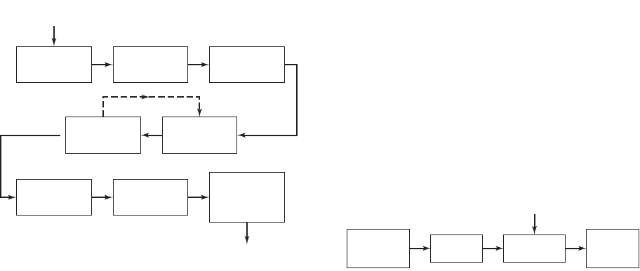
A flowchart of the general electronic design process is shown in Figure PR2.3. This
chart can apply to an entire system or to an individual circuit. A set of specifications
is developed for each electronic system, and then each system is divided into many
simpler circuits. For example, one relatively simple electronic system may be a high
temperature warning indicator. If the temperature of an engine or a particular engine
part becomes greater than some predetermined value, a warning light would go on in
the cockpit.
Initial design approaches are considered and a circuit configuration is proposed,
based on the experience and creativity of the circuit design engineer. This is where
experience in the analysis of many different types of electronic circuits becomes
important. Knowledge of particular characteristics, such as input impedance, output
impedance, gain characteristics, and bandwidth, for many types of circuits, is used to
choose a particular circuit configuration.
Figure PR2.4 shows a block diagram for a particular circuit configuration that
can serve as a starting point for the design of the temperature indicator. The block
showing the amplifier may be further divided to show a proposed configuration for
the circuit. Component values can then be chosen.
Problem
statement
Develop
specifications
Initial design
approach
Develop block
diagram
Performance
simulation
Design of
each block
Prototype
construction
Prototype
testing
Final design
and
construction
Working
system
Figure PR2.3 Flowchart of the design process
Preset
value
Temperature
transducer
Amplifier Comparator
Warning
light
Figure PR2.4 Block diagram of a temperature
warning light circuit
nea80644_pro02_615-618.qxd 06/15/2009 03:54 PM Page 617 F506 Hard disk:Desktop Folder:MHDQ134-PROL-PRII: