Neamen D. Microelectronics: Circuit Analysis and Design
Подождите немного. Документ загружается.


Figure 12.29 Example of a discrete
transistor series–series feedback circuit
R
L
R
C
R
E
V
fb
+
–
+
–
R
if
R
of
I
o
V
i
V
o
R
B
=
R
1
⎪⎪
R
2
g
m
V
p
V
p
r
p
+
–
Figure 12.30 Small-signal equivalent circuit, discrete
transistor series–series feedback configuration
v
i
v
o
C → ∞
C → ∞
V
CC
R
2
R
E
R
L
R
C
R
1
i
o
+
+
–
–
v
fb
v
be
+
–
the amplifier. Assuming the collector and emitter currents are nearly equal and R
i
is
very large, we can write that
I
o
=
V
fb
R
E
= h
FE
I
b
= h
FE
A
g
V
ε
(12.73)
Also,
V
ε
= V
i
− V
fb
= V
i
− I
o
R
E
(12.74)
Substituting Equation (12.74) into Equation (12.73) yields
I
o
= h
FE
A
g
(V
i
− I
o
R
E
)
(12.75)
which can be rearranged to yield the closed-loop transfer function,
A
gf
=
I
o
V
i
=
(h
FE
A
g
)
1 + (h
FE
A
g
)R
E
(12.76)
which has the same form as that of the ideal theory. In this example, we see that in
this feedback network, the transistor current gain is part of the basic amplifier gain.
Discrete Circuit Representation
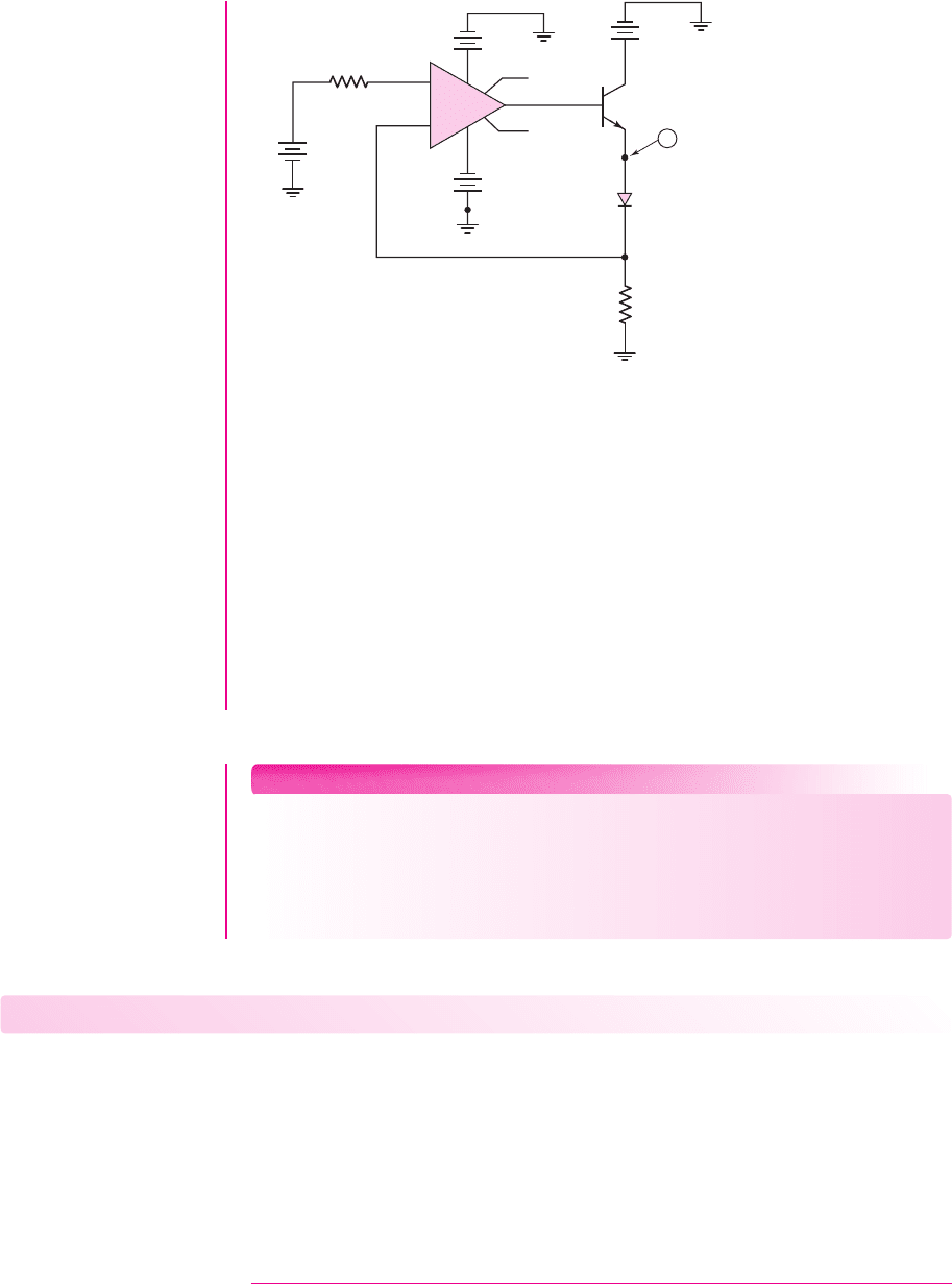
Figure 12.29 shows a single bipolar transistor circuit that is an example of a series–
series feedback configuration. This circuit is similar to those evaluated in Chapters
5 and 6. The input signal is the input voltage v
i
, the feedback voltage is
v
fb
, and the
error signal is the base–emitter voltage. The series output connection samples the
output current; therefore, the feedback voltage is a function of the output current.
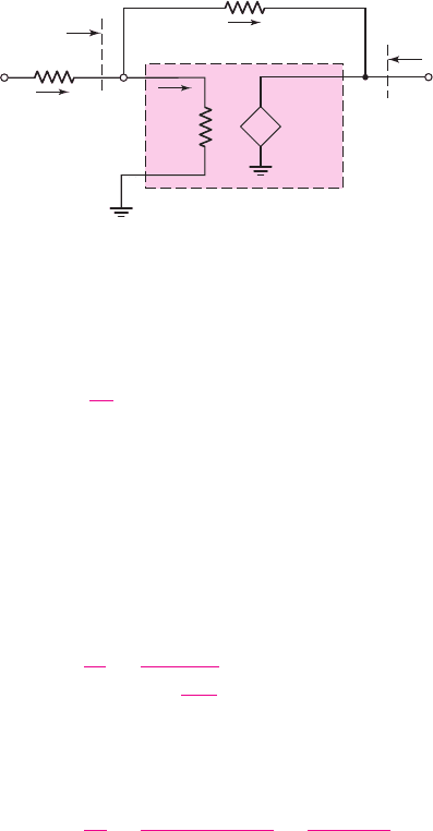
The small-signal equivalent circuit is shown in Figure 12.30. The Early voltage
of the transistor is assumed to be infinite. The output current can be written
I
o
=−(g
m
V
π
)
R
C
R
C
+ R
L
(12.77)
12.6.2
888 Part 2 Analog Electronics
nea80644_ch12_851-946.qxd 6/23/09 1:45 PM Page 888 pmath DATA-DISK:Desktop Folder:23/06/09:MHDQ134-12:

and the feedback voltage is
V
fb
=
V
π
r
π
+ g
m
V
π
R
E
(12.78)
A KVL equation around the B–E loop yields
V
i
= V
π
+ V
fb
= V
π
1 +
1
r
π
+ g
m
R
E
(12.79)
Solving Equation (12.79) for
V
π
, substituting that into Equation (12.77), and
rearranging terms produces the expression for the transconductance transfer
function,
A
gf
=
I
o
V
i
=
−g
m
R
C
R
C
+ R
L
1 +
1
r
π
+ g
m
R
E
(12.80)
Again, the closed-loop transfer function of the discrete transistor feedback
circuit cannot be put in exactly the same form as that of the ideal series–series feed-
back network. Resistor R
C
introduces loading on the output, and
r
π
introduces load-
ing on the input. If both R
C
and
r
π
become large, then Equation (12.80) changes to
the ideal form, where the feedback transfer function is
β
z
=−R
E
and the basic
amplifier transconductance is
A
g
=−g
m
.
EXAMPLE 12.11
Objective: Determine the transconductance gain of a transistor feedback circuit.
Consider the circuit in Figure 12.29, with transistor parameters
h
FE
= 100
,
V
BE
(on) = 0.7
V, and
V
A
=∞
. The circuit parameters are:
V
CC
= 10
V,
R
1
=
55 k
,
R
2
= 12 k
,
R
E
= 1k
,
R
C
= 4k
, and
R
L
= 4k
.
Solution: From a dc analysis of the circuit, the quiescent values are
I
CQ
=
0.983
mA and
V
CEQ
= 5.08
V. The transistor small-signal parameters are found to be
r
π
= 2.64
k
and
g
m
= 37.8
mA/V.
From Equation (12.80), the transconductance transfer function is
A
gf
=
−(37.8)
4
4 + 4
1 +
1
2.64
+37.8
(1)
=−0.482 mA/V
As a first approximation, we have
A
gf
=
1
β
z
=
1
−R
E
=
1
−1k
=−1 mA/V
The term
R
C
/(R
C
+ R
L
)
introduces the largest discrepancy between the actual and
ideal transconductance values.
Chapter 12 Feedback and Stability 889
nea80644_ch12_851-946.qxd 6/23/09 1:45 PM Page 889 pmath DATA-DISK:Desktop Folder:23/06/09:MHDQ134-12:

This circuit is often used as a voltage amplifier. The output voltage is directly
proportional to the output current. Therefore,
A
v f
=
v
o
v
i
=
i
o
R
L
v
i
= A
gf
R
L
which yields
A
v f
= (−0.482)(4) =−1.93
Comment: The circuit in Figure 12.29 is an example of a series–series feedback
topology, even though in many cases we treat this circuit as a voltage amplifier.
When an emitter resistor is included, the small-signal voltage gain decreases,
because of the feedback effect of R
E
. However, the transconductance and voltage
gain become insensitive to the transistor parameters, also a result of the feedback
effect of R
E
. A 100 percent increase in the transistor current gain
h
FE
produces a 0.5
percent change in the closed-loop voltage gain.
EXERCISE PROBLEM
Ex 12.11: For the circuit in Figure 12.31, the transistor parameters are
K
n
= 2
mA/V
2
,
V
TN
= 2
V, and
λ = 0
. (a) Determine (i)
I
DQ
and (ii) the
transconductance transfer function
A
gf
= i
o
/v
i
. (b) If the conductance parameter
decreases by 10 percent to
K
n
= 1.8
mA/V
2
, determine (i) the new value of
I
DQ
and (ii) the percent change in
A
gf
. (Ans. (a) (i)
I
DQ
= 2.31
mA, (ii)
A
gf
=
−0.7904
mA/V; (b) (i)
I
DQ
= 2.22
mA, (ii)
−2.68%)
890 Part 2 Analog Electronics
C → ∞
C → ∞
R
D
= 2 kΩ
R
S
=
0.4 kΩ
R
L
=
2 kΩ
R
1
= 30 kΩ
R
2
=
20 kΩ
+5 V
–5 V
v
i
i
o
+
–
Figure 12.31 Figure for Exercise Ex 12.11
The input resistance
R
if
of the series input feedback connection includes R
E
multiplied by
(1 + h
FE
)
, where h
FE
is the transistor current gain. The input resis-
tance increases significantly because of the series connection.
The output resistance of a series output feedback connection is usually very
large. However, resistance R
C
reduces the output resistance and introduces a loading
nea80644_ch12_851-946.qxd 6/23/09 1:45 PM Page 890 pmath DATA-DISK:Desktop Folder:23/06/09:MHDQ134-12:

effect. The reduced output resistance demonstrates that discrete transistor feedback
circuits do not conform exactly to ideal feedback circuits. Nevertheless, overall cir-
cuit characteristics improve when feedback is used.
DESIGN EXAMPLE 12.12
Objective: Design a driver amplifier to supply current to an LED.
Specifications: The available voltage source is variable from 0 to 5 V and has an
output resistance of
200
. The required diode current is 10 mA when the maximum
input voltage is applied. The required closed-loop transconductance gain is then
A
gf
= I
o
/V
i
= (10 ×10
−3
)/5 → 2mS
.
Choices: An op-amp with the characteristics described in Example 12.8 and a BJT
with
h
FE
= 100
are available.
Solution (Design Approach): To minimize loading effects on the input, an amplifier
with a large input resistance is required; to minimize loading effects on the output,
a large output resistance is required. For these reasons, a series–series feedback
configuration, or transconductance amplifier, is selected.
The closed-loop gain is
A
gf
= 2 ×10
−3
∼
=
1/β
z
and the resistance feedback transfer function is
β
z
= 500
The dependent open-loop voltage source of the op-amp, as shown in Figure 12.17,
can be transformed to an equivalent dependent op-loop transconductance source for
the transconductance amplifier, as shown in Figure 12.12. We find that
A
g
= A
v
/R
o
The parameters specified for the op-amp yield
A
g
= 100 A/V
The loop gain for the series–series configuration is
A
g
β
z
= (100)(500) = 5 × 10
4
Referring to Table 12.1, the expected input resistance is
R
if
= (10)(5 ×10
4
) k → 500 M
and the expected output resistance is
R
of
= (100)(5 ×10
4
)→ 5M
These input and output resistances should minimize any loading effects at the ampli-
fier input and output.
For this example, we may use the amplifier configuration shown in Figure 12.27,
in which the load resistor R
L
is replaced by an LED. In the ideal case,
β
z
= R
E
= 500
Chapter 12 Feedback and Stability 891
nea80644_ch12_851-946.qxd 6/23/09 1:45 PM Page 891 pmath DATA-DISK:Desktop Folder:23/06/09:MHDQ134-12:
Computer Simulation Verification: Figure 12.32 shows the circuit used in the
computer simulation. Again, a standard
μA-741
op-amp was used in the circuit and
a standard diode was used in place of an LED. When the input voltage reached 5 V,
the current through the diode was 10.0 mA, which was the design value. The input
resistance
R
if
was found to be approximately
2400 M
and the output resistance
R
of
was found to be approximately
60 M
. Both of these values are larger than pre-
dicted because of the differences in the assumed op-amp parameters and those of the
μA-741
op-amp.
Comment: Again, an almost ideal feedback circuit can be designed by using an
op-amp.
EXERCISE PROBLEM
*Ex 12.12: Design a transconductance feedback amplifier with a gain of
A
gf
=
10
mS. The source resistance is
R
S
= 500
, and the load is an LED. State any
necessary assumptions. Use an op-amp with the characteristics described in
Example 12.8. From a computer simulation analysis, determine the closed-loop
transconductance, input resistance, and output resistance of your design.
Test Your Understanding
TYU 12.10 Consider the op-amp circuit in Figure 12.27 with parameters
R
E
= 1
k
and
A
g
= 10
2
mA
/
V. Assume the transistor current gain is
h
FE
= 180
. The input
voltage is
V
i
= 1.5
V. (a) (i) Determine the transfer function
A
gf
= I
o
/V
i
and the
output current
I
o
. (ii) Determine the value of the error voltage
V
ε
. (b) If the transis-
tor current gain decreases by 20 percent to
h
FE
= 144
, (i) determine the new values
of
A
gf
and
I
o
, and the percent change in these values and (ii) determine the new
value of
V
ε
. (Ans. (a) (i)
A
gf
= 0.9999444
mA
/
V,
I
o
= 1.4999166
mA, (ii)
V
ε
=
83.4 μ
V; (b) (i)
A
gf
= 0.9999306
mA
/
V,
I
o
= 1.4998959
mA,
−0.00138%
change,
(ii)
V
ε
= 104 μ
V)
892 Part 2 Analog Electronics
–
+
0 V
200 Ω
500 Ω
2
3
7
5
I
0
0
10 V
10 V
10 V
0
0
6
1
4
0
v
1
v
2
v
3
v
4
v–
v+
U
1
mA – 741
R
S
R
E
o
S2
o
S1
Q
1
2N3904
D
1
1N914
+
–
+
–
+
–
+
–
Figure 12.32 Circuit used in the computer simulation analysis for Example 12.12
nea80644_ch12_851-946.qxd 6/23/09 1:45 PM Page 892 pmath DATA-DISK:Desktop Folder:23/06/09:MHDQ134-12:

12.7 TRANSRESISTANCE (SHUNT–SHUNT)
AMPLIFIERS
Objective: • Analyze op-amp and discrete transistor circuit examples
of shunt–shunt (transresistance) feedback amplifiers.
In this section, we will analyze an op-amp and a discrete circuit representation of the
shunt–shunt feedback amplifier. The shunt-shunt circuit is a transresistance ampli-
fier; therefore, we must derive the output voltage to input current transfer function.
For the ideal configuration, this function is given by Equation (12.40) as
A
zf
=
A
z
(1 + β
g
A
z
)
where A
z
is the basic amplifier transresistance gain, and
β
g
is the feedback transfer
function. With this feedback connection, both the input and output resistance
decrease compared to the basic amplifier values.
Op-Amp Circuit Representation
Figure 12.33(a) shows the basic inverting op-amp circuit that we analyzed in Chapter 9.
We treated this as a voltage amplifier whose voltage gain is
A
v
=−V
o
/V
i
. However,
this circuit is actually an example of a shunt–shunt configuration. The defining input
signal is the input current I
i
.
Figure 12.33(b) shows the same circuit without the input resistance. From this
configuration, we see the input shunt connection. The input current splits between the
feedback current
I
fb
and the error current
I
ε
. The shunt output connection samples
the output voltage; therefore, the feedback current is a function of the output voltage.
In the ideal feedback circuit, the amplification factor A
z
is very large, and the
transresistance transfer function is, from Equation (12.40),
A
zf
=
V
o
I
i
∼
=
1
β
g
(12.81)
For the ideal inverting op-amp circuit, V
1
is at virtual ground, and
V
o
=−I
fb
R
2
Also for the ideal op-amp,
I
fb
= I
i
, and the ideal transresistance transfer function is
A
zf
=
V
o
I
i
=−R
2
(12.82)
12.7.1
Chapter 12 Feedback and Stability 893
–
+
V
o
V
i
I
e
I
i
I
fb
V
1
A
R
2
R
1
R
if
R
of
–
+
V
o
I
e
I
i
I
fb
R
2
(a) (b)
Figure 12.33 (a) The basic inverting op-amp circuit and (b) the circuit showing the shunt
input connection
nea80644_ch12_851-946.qxd 6/23/09 1:45 PM Page 893 pmath DATA-DISK:Desktop Folder:23/06/09:MHDQ134-12:
Comparing Equation (12.82) to Equation (12.81), we see that the feedback
transfer function for the ideal inverting op-amp circuit is
β
g
=−
1
R
2
(12.83)
We can take a finite amplifier gain into account by considering the equivalent
circuit in Figure 12.34. The parameter
A
z
is the open-loop transresistance gain fac-
tor, and is negative since the error current
I
ε
is considered to be positive entering the
inverting terminal. We can write
V
o
= A
z
I
ε
=−
|
A
z
|
I
ε
,
I
ε
= I
i
− I
fb
, and
V
o
=
A
z
I
i
− I
fb
=−
|
A
z
|
I
i
− I
fb
. If we assume that voltage
V
1
is at virtual ground,
then
I
fb
=−V
o
/R
2
. Combining equations, we see that the closed-loop transresis-
tance transfer function is
A
zf
=
V
o
I
i
=
−
|
A
z
|
1 +
|
A
z
|
R
2
(12.84)
From Equation (12.83), the feedback transfer function is
β
g
=−1/R
2
, and Equation
(12.84) becomes
A
zf
=
V
o
I
i
=
−
|
A
z
|
1 + (−
|
A
z
|
)β
g
=
A
z
1 + A
z
β
g
(12.85)
This feedback circuit is one example in which the open-loop gain of the basic am-
plifier,
A
z
= V
o
/I
ε
, is negative. The feedback transfer function,
β
g
=−1/R
2
, is also
negative, but the loop gain
T = A
z
β
g
is positive for this negative feedback circuit.
The transresistance transfer function for the inverting op-amp circuit has the
same form as that for the ideal shunt–shunt configuration. In addition, since V
1
is at
virtual ground, the input resistance including feedback,
R
if
, is essentially zero, and
we have shown that the output resistance with feedback,
R
of
, is very small. These
small resistance values are a result of the shunt–shunt configuration. Therefore, our
analysis of the inverting op-amp circuit produces results consistent with ideal
shunt–shunt feedback characteristics.
The inverting amplifier circuit in Figure 12.33 is most often thought of as a volt-
age amplifier. The input current I
i
is directly proportional to the input voltage V
i
,
which means that the voltage transfer function (gain) and transresistance transfer
function have the same characteristics. Even though we are usually concerned with
the voltage gain, the inverting amplifier is an example of a shunt–shunt feedback
topology which is a transresistance amplifier.
894 Part 2 Analog Electronics
A
oL
V
d
= A
z
I
e
= -| A
z
|I
e
V
i
V
o
R
i
V
d
R
2
I
i
V
1
I
fb
–
+
–
+
R
if
R
of
I
e
R
1
+
–
Figure 12.34 Equivalent circuit, op-amp shunt–shunt feedback configuration
nea80644_ch12_851-946.qxd 6/23/09 1:45 PM Page 894 pmath DATA-DISK:Desktop Folder:23/06/09:MHDQ134-12:
Discrete Circuit Representation
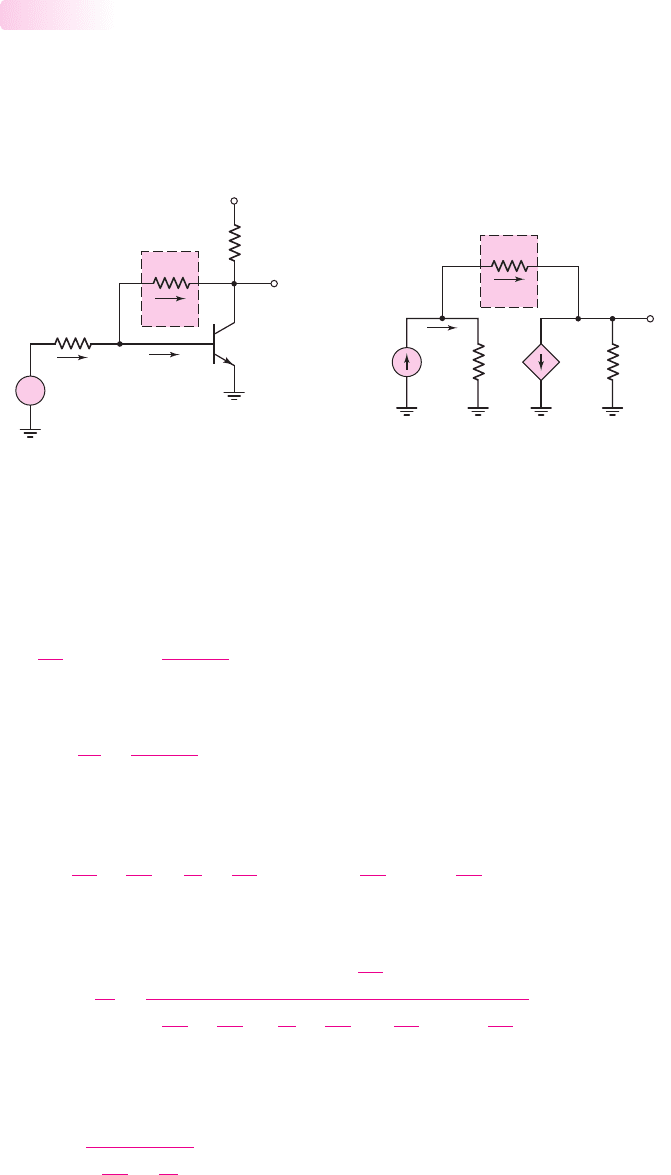
Figure 12.35 shows a single bipolar transistor circuit, which is an example of a
shunt–shunt feedback configuration. The input signal current is i
i
, the feedback current
is
i
fb
, and the error signal current is
i
ε
and is the signal base current. The shunt output
samples the output voltage; therefore, the feedback current is a function of v
o
.
12.7.2
Chapter 12 Feedback and Stability 895
v
i
v
o
R
C
R
F
R
S
V
CC
i
fb
i
e
i
i
+
–
Figure 12.35 Example of a discrete transistor
shunt–shunt feedback circuit
Figure 12.36 Small-signal equivalent
circuit, discrete transistor shunt–shunt
feedback configuration
I
i
V
o
R
F
I
fb
+
–
g
m
V
p
V
p
r
p
I
e
R
C
The small-signal equivalent circuit is shown in Figure 12.36. The input signal is
assumed to be an ideal signal current source. Also the Early voltage of the transistor
is assumed to be infinite.
Writing a KCL equation at the output node, we find
V
o
R
C
+ g
m
V
π
+
V
o
− V
π
R
F
= 0
(12.86)
A KCL equation at the input node yields
I
i
=
V
π
r
π
+
V
π
− V
o
R
F
(12.87)
Solving Equation (12.87) for
V
π
and substituting that result into Equation (12.86),
we obtain
V
o
1
R
C
+
1
R
F
1
r
π
+
1
R
F
+
g
m
−
1
R
F
I
i
+
V
o
R
F
= 0
(12.88)
The transresistance transfer function is then
A
zf
=
V
o
I
i
=
−
g
m
−
1
R
F
1
R
C
+
1
R
F
1
r
π
+
1
R
F
+
1
R
F
g
m
−
1
R
F
(12.89)
The open-loop transresistance gain factor A
z
is found by setting
R
F
=∞
.
We find
A
z
=
−g
m
1
R
C
1
r
π
=−g
m
r
π
R
C
=−h
FE
R
C
(12.90)
nea80644_ch12_851-946.qxd 6/23/09 1:45 PM Page 895 pmath DATA-DISK:Desktop Folder:23/06/09:MHDQ134-12:

where
h
FE
is the common-emitter transistor current gain. Multiplying both numer-
ator and denominator of Equation (12.89) by (
r
π
R
C
), we obtain the closed-loop
transresistance gain,
A
zf
=
V
o
I
i
=
+
A
z
+
r
π
R
C
R
F
1 +
R
C
R
F
1 +
r
π
R
F
−
1
R
F
A
z
+
r
π
R
C
R
F
(12.91)
The closed-loop transresistance gain for the single-transistor feedback circuit
cannot be put into the ideal form, as given in Equation (12.40), without further
approximations. In an ideal feedback circuit, the feedback network does not load the
basic amplifier. Also, the forward transmission occurs entirely through the basic am-
plifier. However, in a discrete transistor feedback circuit, these ideal assumptions are
not entirely valid; therefore, the form of the transfer function is usually not exactly
the same as that of the ideal configuration.
We may assume that the feedback resistor is fairly large, which means that the
feedback does not drastically perturb the circuit. We may then assume
h
FE
= g
m
r
π
(r
π
/R
F
)
If we also assume that
R
C
R
F
and
r
π
R
F
, then Equation (12.91) reduces to
A
zf
=
V
o
I
i
∼
=
A
z
1 + (A
z
)
−1
R
F
(12.92)
Consequently, the feedback transfer function is approximately
β
g
∼
=
−1
R
F
(12.93)
Equation (12.93) demonstrates that the approximate value of the feedback transfer
function depends only on a resistance value.
Although the actual closed-loop transfer function does not fit the ideal form, the
magnitude of that function depends less on the individual transistor parameters than
does the open-loop gain. This characteristic is one of the general properties of feed-
back circuits.
Also, since the input current is proportional to the input voltage, we can use this
circuit as a voltage amplifier.
EXAMPLE 12.13
Objective: Determine the transresistance and voltage gain of a single-transistor
shunt–shunt feedback circuit.
Consider the circuit in Figure 12.37(a). The transistor parameters are:
h
FE
= 100
,
V
BE
(on) = 0.7
V, and
V
A
=∞
. Since the input signal current is directly proportional
to the input voltage, the voltage gain of this shunt–shunt configuration has the same
general properties as the transresistance transfer function.
As with many circuits considered in this chapter, several capacitors are included.
In the circuit in Figure 12.37(a), R
1
and C
C2
may be removed. Resistor R
F
can be
used for biasing, and the circuit can be redesigned to provide the same feedback
properties.
896 Part 2 Analog Electronics
nea80644_ch12_851-946.qxd 6/24/09 10:33 AM Page 896 pmath DATA-DISK:Desktop Folder:24/06/09:MHDQ134-12:
Solution: By including C
C2
in the circuit, the feedback is a function of the ac signal
only, which means that the transistor quiescent values are not affected by feedback.
The quiescent parameters are found to be
I
CQ
= 0.492
mA and
V
CEQ
= 5.08
V, and
the small-signal parameters are
r
π
= 5.28 k
and
g
m
= 18.92
mA/V.
In the small-signal equivalent circuit, which is shown in Figure 12.37(b), the
Thevenin equivalent input source is converted to a Norton equivalent circuit. Writing
a KCL equation at the output, we obtain
V
o
10
+(18.9)V
π
+
V
o
− V
π
82
= 0
A KCL equation at the input yields
I
i
=
V
π
10
+
V
π
4.96
+
V
π
5.28
+
V
π
− V
o
82
Combining these two equations and eliminating
V
π
, we find the small-signal trans-
resistance gain, which is
A
zf
=
V
o
I
i
=−65.87 k
Since this unit of gain is not as familiar as voltage gain, we determine the volt-
age gain from
I
i
= V
i
/R
S
= V
i
/10
Chapter 12 Feedback and Stability 897
(a)
+
–
R
2
= 5.5 kΩ
R
E
= 0.5 kΩ
R
1
= 51 kΩ
R
C
= 10 kΩ
V
CC
= 10 V
+
–
C
E
→ ∞
R
if
R
of
R
S
= 10 kΩ
C
C1
→ ∞
C
C2
→ ∞
R
F
= 82 kΩ
1
7
3
6
2
4
5
v
i
v
o
(b)
R
F
= 82 kΩ
R
C
=
10 kΩ
R
S
=
10 kΩ
18.9V
p
(mA)
+
–
V
p
r
p
=
5.28 k
Ω
R
1
⎪⎪
R
2
=
4.96 k
Ω
V
o
V
i
R
S
=I
i
Figure 12.37 (a) Circuit for Example 12.13 and (b) small-signal equivalent circuit
nea80644_ch12_851-946.qxd 6/23/09 1:45 PM Page 897 pmath DATA-DISK:Desktop Folder:23/06/09:MHDQ134-12: