Graef M. Introduction to conventional transmission electron microscopy
Подождите немного. Документ загружается.


228 The transmission electron microscope
phosphor screen is about 50 µm (the smallest detail that can be resolved on the
screen depends on the phosphor grain size). The apparent image brightness on the
viewing screen depends on the microscope acceleration voltage (a higher voltage
corresponds to a dimmer image) and on the thickness of the lead glass viewing
window.
3.11.3 Photographic emulsions
Photographic emulsions are perhaps the most commonly used electron detectors.
Although digital detection systems are becoming increasingly important, it is doubt-
ful that photographic film will be replaced completely in the near future by purely
digital systems. In this section, we will describe briefly how a photographic emul-
sion reacts to an incident electron and how one may extract quantitative information
from the exposed and developed negative.
When an incident electron beam with current density j
0
hits a photographic
emulsion, then the total exposure E is defined as the product of current density
(also known as illuminance) and exposure time τ:
E = j
0
τ.
The energy of the absorbed electrons locally converts at least one and often more
than one silver halide grains into metallic silver. Those regions of the emulsion that
have been converted to metallic silver are then developed, which essentially means
that the entire halide grain is converted to metallic silver by a suitable reducing
agent (i.e. the developer). Grains that have not been exposed are then removed
by the fixing or fixation process, and the exposed regions appear as dark patches
on the transparent acetate support film. For extensive details on the theory of the
photographic process we refer the interested reader to the book Fundamentals of
Photographic Theory by James and Higgins [JH68].
When the developed negative is illuminated by a light source of intensity I
0
,a
fraction I (x, y) is transmitted, depending on the density of metallic silver at the
location (x, y). We define the photographic density D by
D(x, y) = log
10
I
0
I (x, y)
.
The ratio I /I
0
is known as the intensity transmittance of the negative. The pho-
tographic density can be measured by a densitometer or a scanner equipped with
a transparency adapter. Instead of using the actual intensity of the light source as
I
0
, it is often easier to use the scanned intensity from a region near the edge of
the negative (a region which was not exposed to electrons, but underwent the same
development and fixation process as the exposed region).
3.11 Electron detectors 229
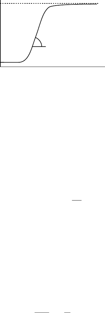
Optical Density D
D
fog
log E
D
max
slope = electron speed k
Fig. 3.44. Schematic representation of the Hurter–Driffield curve, relating optical density
D to the logarithm of the exposure E. The fog level represents the density of an unexposed
but developed region of the negative. The maximum density level is typically
around
D ≈ 3.
The relation between the density D and the exposure E is commonly represented
by a logarithmic plot of D versus log E, known as the Hurter–Driffield curve or the
characteristic curve. A schematic example of such a curve is shown in Fig. 3.44.
For exposure to light, such a curve properly describes the relation between E and
D. Up to a minimum exposure level, the film density is constant and equal to a
small number, known as the fog level. Then the curve becomes linear with slope k,
the film speed, sometimes known as the photographic contrast. Electron speeds for
modern emulsions are in the range 0.3–1.1
µm
2
per electron. For large exposures,
all halide grains are converted into metallic silver and the film saturates at a limiting
density D
max
. The practical value of the saturation density is between D
max
= 2 and
3 for most applications, D = 3 indicating that only
1
1000
of the illuminated intensity
is transmitted through the negative. The precise shape of the characteristic curve
depends in a sensitive way on the experimental conditions during development
and fixation (temperature, time, etc.), and it is not a trivial matter to extract reliable
intensity data from photographic negatives. For an extensive discussion of this topic
the reader is referred to the early work by Frieser, Klein, and Zeitler [FKZ59] and
the more recent approach to quantitative analysis of electron negatives by Campbell,
Cohen and King [CCK97]. Zeitler [Zei92] has shown that for electron exposures
at densities of less than 1.5 the relation between D and E is essentially linear.
It is possible to define and measure the point spread function for an electron
negative. It can be shown (e.g. [Zei92]) that the radially symmetric PSF T (r)is
given by
T (r) =
1
2π x
2
0
K
0
r
x
0
, (3.86)
where K
0
is a modified Bessel function and x
0
is a decay length, which depends on
the electron energy. The corresponding modulation transfer function T (q)isgiven
230 The transmission electron microscope
by the Fourier transform:
T (q) =
1
1 + q
2
x
2
0
. (3.87)
This function has no zero-crossings and can, therefore, be deconvolved from the
recorded transmittance. In practice, such a deconvolution will be performed nu-
merically, which means that the negative must be digitized, either by means of
a densitometer, or by regular scanning using a transparency adapter. Whichever
digitization method is used, the reader should be aware that the scanning device
itself may impose its own modulation transfer function on the digitized image. For
densitometers such an instrumental MTF is well understood and can be determined
easily. For flat-bed scanners on the other hand, the MTF depends on the details of
the illumination and also on the discreteness of the detector array, typically a diode
array.
3.11.4 Digital detectors
Charge-coupled device detectors, commonly known as CCD detectors, have been
around since 1970, when Boyle and Smith proposed the first charge-coupled semi-
conductor device [BS70]. While there have been many advances in the performance
of CCD detectors since their invention, the basic operational principles have not
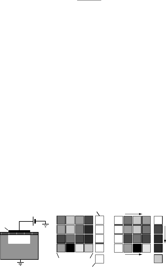
changed significantly. A silicon substrate (Fig. 3.45a) is lightly doped with about
10
15
acceptor atoms cm
−3
so that it acts as a p-type semiconductor. A thin (100
nm) silicon dioxide layer is deposited on top of the substrate, followed by a metal
gate. When a positive voltage is applied to the gate the majority carriers, holes in
the case of a p-type semiconductor, are repelled from the area underneath the gate
V
SiO
2
Metal gate
p-type Si
depletion
region
shift all
elements
Active detector
area
read-out
circuitry
extra column
(a) (b) (c)
Fig. 3.45. (a) Schematic representation of the structure of a single element of a CCD device;
(b) all elements of a 4 × 4 detector array are exposed to incident light; (c) the array is first
shifted one element to the right, and then the elements of the vertical column are shifted
into the read-out circuitry. Then the array is shifted again, until all elements have passed
through the read-out circuitry.
3.11 Electron detectors 231
and a depletion layer is formed. The bias voltage therefore creates a potential well,
the depth of which is determined by the bias voltage, the thickness of the oxide
layer and the size of the metal contact [BL80]. This potential well can subsequently
be filled with minority carriers (electrons), which will form a thin layer close to
the oxide. As the number of electrons increases, the depletion region shrinks, until
a maximum number of electrons has been accumulated. At this point the potential
well is saturated and can accept no additional electrons.
When an array of CCD elements is exposed to light, the potential wells will be
filled with electrons, and the number of electrons in each well will be proportional
to the incident light intensity for that particular well. Once the exposure has been
completed, the charge in each CCD element must be determined. This is accom-
plished by a clever combination of voltage changes applied to neighboring detector
elements. For a detailed discussion of this mechanism as well as a description of
other CCD geometries we refer to [BL80] or [HM79]. All the charges accumulated
along a line of CCD elements are simultaneously shifted one element sideways
(Fig. 3.45b), and the final column is shifted down towards the read-out circuitry
which measures the total charge in each individual element (Fig. 3.45c). When all
elements have been read, the CCD device is ready for the next exposure.
Scientific CCD detectors are typically square detectors, with element sizes in the
range of 10–25
µm on the side. For TEM imaging, the beam electrons are first con-
verted into photons in a phosphor or YAG (yttrium aluminum garnet) scintillator.
Subsequently, the photons hit the active area of the CCD elements and generate
electrons that fill the potential wells in the depleted regions of the p-type semicon-
ductor. The scintillator is coupled to the CCD detector array through a fiber-optic
coupling, or is directly cemented onto the array. To reduce electronic noise, CCD de-
tectors are cooled down to the range −30 to −50
◦
C using Peltier cooling elements.
The dominant sources of noise are in the scintillator electron–photon conversion
and the detector photon–electron conversion processes.
Modern CCD detectors can have as many as 4096 × 4096 detector elements, and
each element has a dynamic range of 12, 14, or 16 bits. A single image from such
a detector will occupy 32 megabytes (33 554 432 bytes) of memory or disk space.
File compression algorithms may be used to reduce the file size, but care must be
taken to use only lossless compression algorithms when raw image data is stored.
†
Image analysis should only be performed on raw image data, not on data that has
been stored using a lossy compression algorithm.
The imaging characteristics of a CCD detector are well described using the MTF
formalism introduced in Section 3.11.1.2. For a rather complete description of the
†
Lossless image compression is typically available in the tagged image file format, or tiff -format. Lossy image
compression algorithms are used for the Joint Photographic Experts Group format, or jpeg-format.
232 The transmission electron microscope
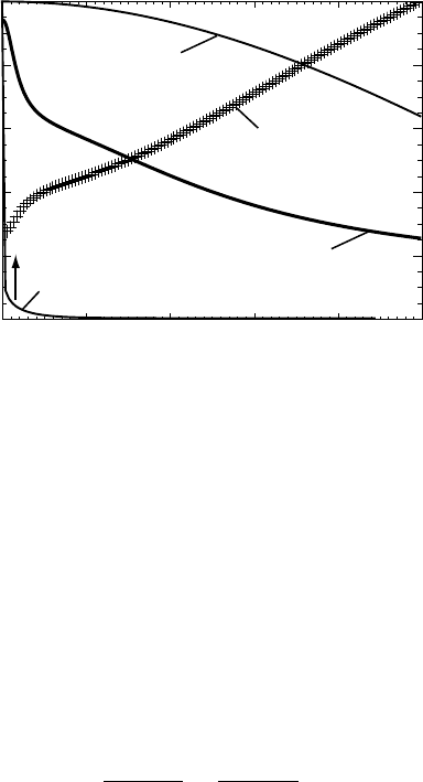
1.0
0.8
0.6
0.4
0.2
0.0
0.0 0.1 0.2 0.3 0.4 0.5
Frequency (1/pixels)
MTF (PSF)
ideal MTF for
square pixel detector
Gatan 679
slow-scan
CCD at 120 kV
inverse MTF
normalized PSF
Pixels (for PSF)
0 1020304050
Fig. 3.46. Modulation transfer function for a 1 K × 1 K Gatan 679 slow-scan CCD camera
with a 120 kV incident electron beam
[Zuo96]. The inverse of the MTF (MTF
max
/MTF) is
also shown, along with the ideal MTF for a signal lined up with one of the rows or columns
of a square detector array. The bottom curve is the normalized point spread function T (r)
versus distance measured in pixels (scale on top).
imaging characteristics of CCD cameras we refer the interested reader to de Ruijter
[dR95] and Zuo [Zuo96]. In this section, we will only state the most important facts.
The MTF of a CCD camera is similar in form to that of a photographic negative.
Zuo [Zuo96] has modeled slow-scan CCD cameras with different scintillators at
different microscope acceleration voltages using the following MTF:
T (q) =
a
1 + αq
2
+
b
1 + βq
2
+ c, (3.88)
where the first two terms model the head and tail part of the point spread function
and c is a constant. Figure 3.46 shows an example MTF for a Gatan model 679
slow-scan CCD camera operated at 120 kV. The camera has 1024 × 1024 pixels
with a dynamic range of 12 bits, a YAG scintillator, and Peltier cooling to −30
◦
C.
The fitting coefficients are a = 0.3293, α = 3328.8, b = 0.46423, β = 13.511,
and c = 0.147 94
†
[Zuo96]. The frequency range goes from zero to the Nyquist
frequency q
c
; in other words, the frequency axis is labeled in units of the sampling
rate.
†
The reader should note that these are approximate parameters; at zero frequency, the MTF should be equal to
unity, or a + b + c = 1, and for the case shown we have a + b + c = 0.941 47.

Exercises 233
The corresponding point spread function consists of two modified Bessel func-
tions K
0
plus a delta-function (the Fourier transform of the constant c):
T (r) =
1
2πα
K
0
r
√
α
+
1
2πβ
K
0
r
√
β
+ cδ(r), (3.89)
which is a sharply peaked function with a slowly decaying tail. For the fitting pa-
rameters introduced above, 85% of the area under the PSF falls within the first
six pixels, while 99% falls within the first 30 pixels. This indicates that an in-
cident electron has an 85% probability to be detected inside a circle with radius
six pixels centered on the point of impact on the scintillator. The main conse-
quence of the point spread function is that the highest spatial frequencies are
suppressed with respect to the low spatial frequencies, and this in turn causes
sharp features in the image to be smoothed. The inverse MTF, also shown in
Fig. 3.46, can be used to deconvolve the PSF from the image. Care must be
taken that the various operations in equation (3.84) are performed in the proper
order.
The detective quantum efficiency, DQE, is in the range 0.5–0.7 for electron doses
between 100 and 1000 counts pixel
−1
. For explicit expressions for the frequency-
dependent DQE (DQE(µ, ν)) we refer to [dR95] and [Zuo96]. It can also be shown
from experimental measurements that the number of CCD well electrons is be-
tween 10 and 30 per incident beam electron, depending on the details of the
scintillator.
Exercises
3.1 Derive the paraxial radial trajectory equation (3.17).
3.2 Use the
lens.f90 program to determine an empirical relation between a and B
0
(for
Glaser’s bell-shaped field) for which the lens
has the so-called
“telescopic property”,
i.e. the incident and exciting trajectories are both parallel to the optical axis, but at
a different distance from the axis. Such a lens would change the beam diameter of a
cylindrical beam.
3.3 Use the
lens.f90 program to create a configuration consisting of two unequal lenses
which, for a given acceleration voltage, will produce an exit trajectory at half the
distance from the optical axis (i.e. r (z
i
) ≈ 0.5r(z
0
) and r
(z
i
) = 0.0) and which has
zero total image rotation.
3.4 Derive the components of the lens transfer matrix (3.29).
3.5 Verify graphically that the image Q of the object point P will be magnified when the
object is located at a distance shorter than the object focal length from the object focal
plane (see Fig. 3.9 and the discussion on page 160).
3.6 Draw ray diagrams similar to the one in Fig. 3.27(b) for the under-focus and over-focus
conditions of the second condensor lens.
234 The transmission electron microscope
3.7 Show that the barrier reduction due to the Schottky effect is given by equation (3.48)
on page 181.
3.8 Equation (3.77) was derived for HOLZ reflections with the incident beam along a
zone axis. If the incident beam is tilted slightly away from the zone axis, so that the
wave vector k
0
acquires the components L
1
and L
2
with respect to the vectors g
1
and
g
2
, what will be the resulting changes to equation (3.77)?
4
Getting started
4.1 Introduction
This chapter covers a wide range of topics, all of which are related to standard,
routine microscope operation. Microscope operation can be divided into three
levels: (1) operations common to all microscope models, regardless of manufac-
turer; (2) operations specific to a particular model; and (3) operations specific to
a particular laboratory or location. In this chapter, we will only deal with the first
kind of operations.
For operations specific to a given microscope model, we refer the reader to
the microscope manual, which comes with every installation. Most manuals are
very detailed, with photographs of microscope components and the layout of the
console. In addition, routine procedures such as specimen exchange, photographic
plate exchange, switching between imaging modes (which buttons to press), and
so forth, are detailed in the microscope manual. For the beginning microscopist, it
is a good idea to keep this manual at hand throughout the first series of microscope
sessions.
In addition, there may be special (local) rules for such things as:
r
specimen and specimen holder handling (where the gloves are, what kind of tweezers
should be used, how the specimen holder should be stored, etc.);
r
how to turn up the filament current (i.e. how much time should be left between subsequent
filament current
increments, should the acceleration voltage be left on between
users, etc.);
r
what type of log should one keep? Is there a general log for all micrographs, or does every
user keep a personal log? How does one sign up for microscope time?
r
in what state should the microscope be left for the next user (e.g. the minimum number of
unexposed plates to be left in the camera, the position of all apertures, the magnification
at which the microscope should be left, etc.).
Such rules are often written up in a laboratory manual, or verbally passed on to new
microscope users. Rather than attempt to cover every possible laboratory situation,
235
236 Getting started
for the remainder of this book we will assume that: (1) the reader has access
to a transmission electron microscope; (2) there is an experienced microscopist or
microscope technician in the laboratory who can be consulted when problems arise;
(3) the microscope manual is at hand; and (4) ample microscope time is available.
The microscope manual and additional local procedures make up what we shall call
the standard procedures manual. The reader is encouraged to become familiar with
all such procedures, and to follow them at all times. Whenever we use statements
such as “switch to diffraction mode” we will assume that the reader can find out
from the standard procedures manual how to do that.
What this chapter does deal with can then be summarized as follows:
r
startup and alignment procedures;
r
basic observation modes;
r
how to take “good” micrographs;
r
microscope calibration;
r
basic preparation to begin observations on a “new” material.
The last item includes thin-foil preparation as well as gathering crystallo-
graphic information concerning the material and producing
a
crystal information
package.
This chapter does not provide the reader with a detailed overview of all possi-
ble thin-foil preparation methods. Specimen preparation is simply too important
to be discussed in only one short chapter. Specimen preparation may take well
over 80% of the overall experimental effort; it is not unusual for a microscopist
to spend five or more times as much time on the specimen preparation part than
on the actual microscopy observations! With the advent of atomic resolution mi-
croscopes and advanced analytical instruments it has become clear that without
a clean, well-prepared foil there is little or no point in reserving time on a mi-
croscope. Conventional TEM techniques are perhaps a bit more forgiving about
the quality of the foil (e.g. foils which are useless for analytical measurements
may still be useful for conventional imaging), but it is always better to invest
time in preparing good foils, regardless of the observations subsequently carried
out on those foils. However, because of overall page limitations, this textbook
does not devote a proportional number of pages to specimen preparation. We re-
fer the reader to one of the following books for a detailed account of various
specimen preparation techniques: Specimen Preparation for Transmission Elec-
tron Microscopy of Materials (P. Goodhew, [Goo84]); the four volumes in the MRS
conference series Specimen Preparation for Transmission Electron Microscopy of
Material [BAM88, And90, ATB92, AW97]; and volume 5 of the original Edington
monographs on Practical Electron Microscopy in Materials Science (difficult to
find but an excellent source, [Edi76]).
4.2 The xtalinfo.f90 program 237
As stated in the Preface on page xiv, one of the main goals of this text is to
provide a good starting point for the microscopy student. The author has selected
four materials from which nearly all micrographs in this book have been obtained.
The materials will be discussed in Section 4.3 and are relatively easy to obtain.
Detailed specimen preparation instructions are included for these four materi-
als, so that the reader may prepare his/her own foils and then reproduce most
of the micrographs in the book. These four materials will also be used in later
chapters for a variety of theoretical and numerical computations of image con-
trast and diffraction features. While this approach limits the range of microstruc-
tural features and defects that are considered, the advantage is that the reader can
practice and compare his/her observations with the images in this book. After a
discussion of specimen preparation for the four study materials, Cu-15 at% Al,
Ti, GaAs, and BaTiO
3
, we conclude the chapter with a series of typical observa-
tions, both in image and diffraction modes. It will then be the primary goal of the
theoretical chapters to explain and model the various contrast features observed,
and to create a framework for the routine simulation of conventional TEM image
contrast.
4.2 The
xtalinfo.f90 program
Whenever one starts to work on a new material, it is useful to gather all the necessary
crystallographic information about this material. In addition, it is often useful to
calculate several relevant, usually low-index, zone axis diffraction patterns. We will
see in Chapter 5 that there are also a few quantities, such as the extinction distance,
which are useful for the interpretation of conventional TEM micrographs.
The program
xtalinfo.f90, available from the website, creates several pages of
PostScript output, listing the most relevant information about the crystal structure
in a form useful to the TEM operator. All of the entries on these pages can be
obtained readily from various public domain and commercial software packages,
but it is convenient to have everything available in one single program, formatted
in a consistent way. The input to the program is the basic crystallographic in-
formation (lattice parameters, space group, and asymmetric unit), the microscope
acceleration voltage and camera length; the output consists of crystallographic in-
formation, structure factor amplitudes, intensities, and extinction distances ranked
by family, stereographic projections for the three basic crystallographic directions
(both direct and reciprocal space projections), and computed electron diffraction
patterns for a series of low-index zone axes (drawn to the correct scale). The pro-
gram combines nearly all of the routines described in Chapters 1 and 2, and for
information on the individual modules we refer to the relevant sections in those
chapters.