Marder M.P. Condensed Matter Physics
Подождите немного. Документ загружается.

Metal Interfaces
573
metals are brought in contact, the regions with excess charge have atomic dimen-
sions.
When semiconductors are brought into contact, charge densities are much
smaller than in metals, and the length scales over which charges build up turn out
to be much larger, as will be shown in Section 19.4.2.
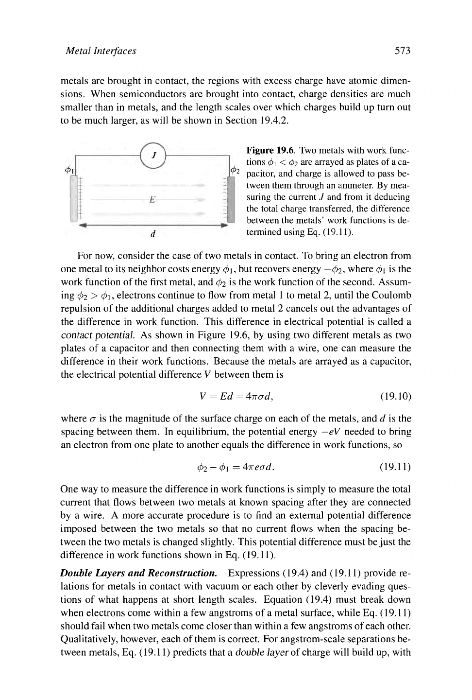
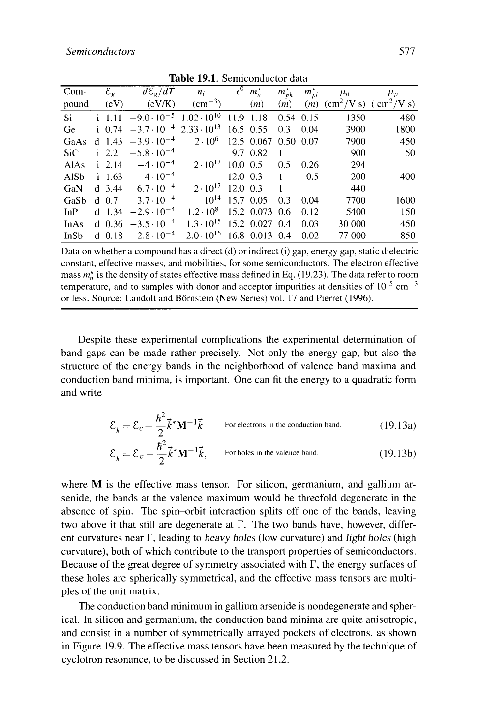
Figure 19.6. Two metals with work func-
tions
4>\
<4>2
are arrayed as plates of
a
ca-
pacitor, and charge is allowed to pass be-
tween them through an ammeter. By mea-
suring the current J and from it deducing
the total charge transferred, the difference
between the metals' work functions is de-
termined using Eq. (19.11).
For now, consider the case of two metals in contact. To bring an electron from
one metal to its neighbor costs energy
4>\,
but recovers energy
—cj)2,
where
<fr\
is the
work function of the first metal, and
(j>2
is the work function of the second. Assum-
ing
4>2
>
4>\,
electrons continue to flow from metal 1 to metal 2, until the Coulomb
repulsion of the additional charges added to metal 2 cancels out the advantages of
the difference in work function. This difference in electrical potential is called a
contact potential. As shown in Figure 19.6, by using two different metals as two
plates of a capacitor and then connecting them with a wire, one can measure the
difference in their work functions. Because the metals are arrayed as a capacitor,
the electrical potential difference V between them is
V = Ed =
4TTad,
(19.10)
where a is the magnitude of the surface charge on each of the metals, and d is the
spacing between them. In equilibrium, the potential energy — eV needed to bring
an electron from one plate to another equals the difference in work functions, so
(j)
2
-</>,=
4-Kead.
(19.11)
One way to measure the difference in work functions is simply to measure the total
current that flows between two metals at known spacing after they are connected
by a wire. A more accurate procedure is to find an external potential difference
imposed between the two metals so that no current flows when the spacing be-
tween the two metals is changed slightly. This potential difference must be just the
difference in work functions shown in Eq. (19.11).
Double Layers and Reconstruction. Expressions (19.4) and (19.11) provide re-
lations for metals in contact with vacuum or each other by cleverly evading ques-
tions of what happens at short length scales. Equation (19.4) must break down
when electrons come within a few angstroms of a metal surface, while Eq. (19.11)
should fail when two metals come closer than within a few angstroms of each other.
Qualitatively, however, each of them is correct. For angstrom-scale separations be-
tween metals, Eq. (19.11) predicts that a double layer of charge will build up, with
574 Chapter 19. Electronics
charge density on the order of 5
•
10
_3
electrons/Â
2
. Compared to the the normal
density of electrons along any surface of a metal, this number is not particularly
large. However, the electric fields involved are on the order of leV/Â, and they
are enormous compared to fields normally generated in the laboratory. The double
layer of surface charges is a dipole layer, and one can view the work function of a
metal generally as arising from the presence of such layers at the surface.
Band structure programs are able to calculate detailed properties of surfaces
with a fair degree of success, and they find such quantities as work functions. Early
work along these directions was described by Lang (1973) and Appelbaum and
Hamann
(
1976),
and a more recent review is given by Zangwill (1988). Because the
computer programs depend upon using Bloch's theorem, they must have a periodic
crystal in which to carry out the calculations. One solution of this difficulty is to
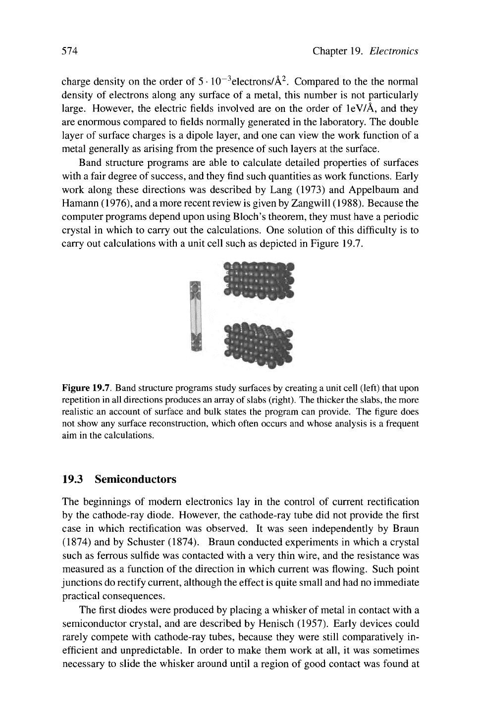
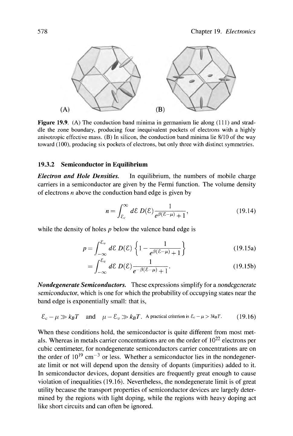
carry out calculations with a unit cell such as depicted in Figure 19.7.
Figure 19.7. Band structure programs study surfaces by creating a unit cell (left) that upon
repetition in all directions produces an array of
slabs
(right).
The thicker
the
slabs, the more
realistic an account of surface and bulk states the program can provide. The
figure
does
not show any surface reconstruction, which often occurs and whose analysis is a frequent
aim in the calculations.
19.3 Semiconductors
The beginnings of modern electronics lay in the control of current rectification
by the cathode-ray diode. However, the cathode-ray tube did not provide the first
case in which rectification was observed. It was seen independently by Braun
(1874) and by Schuster (1874). Braun conducted experiments in which a crystal
such as ferrous sulfide was contacted with a very thin wire, and the resistance was
measured as a function of the direction in which current was flowing. Such point
junctions do rectify current, although the effect is quite small and had no immediate
practical consequences.
The first diodes were produced by placing a whisker of metal in contact with a
semiconductor crystal, and are described by Henisch (1957). Early devices could
rarely compete with cathode-ray tubes, because they were still comparatively in-
efficient and unpredictable. In order to make them work at all, it was sometimes
necessary to slide the whisker around until a region of good contact was found at
Semiconductors
575
random. The progress of basic research into solid-state physics in the 1930s and
late 1940s found the cause of the apparent unpredictability of semiconductors: the
presence of certain crucial impurities in extremely small quantities. Once the role
of these impurities was understood, and methods developed to control them, diodes
and triodes based upon semiconductors took part in a remarkable development that
eventually displaced the cathode-ray tubes that had inspired them, and they led
electronics to a level of extraordinary complexity.
The discussion will begin with the simplest basic physics, and gradually deco-
rate it with additional effects, until the mechanisms responsible for semiconductor
electronics emerge. The starting point is the statistical mechanics of pure semicon-
ductor crystals, followed by statistical mechanics of semiconductor crystals doped
with small quantities of impurities, and finally the theory of conductivity in junc-
tions between differently doped semiconductors.
19.3.1 Pure Semiconductors
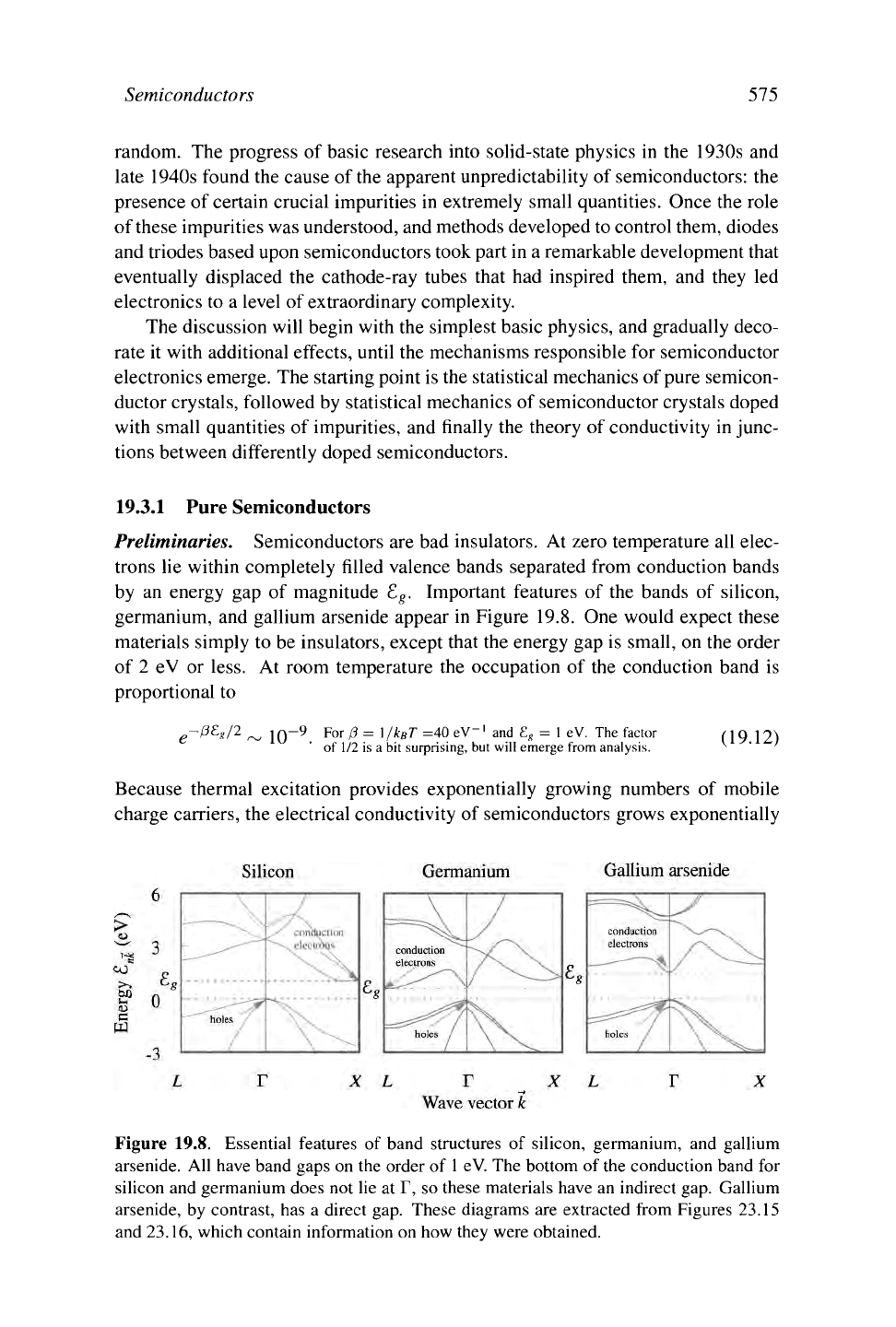
Preliminaries. Semiconductors are bad insulators. At zero temperature all elec-
trons lie within completely filled valence bands separated from conduction bands
by an energy gap of magnitude £
g
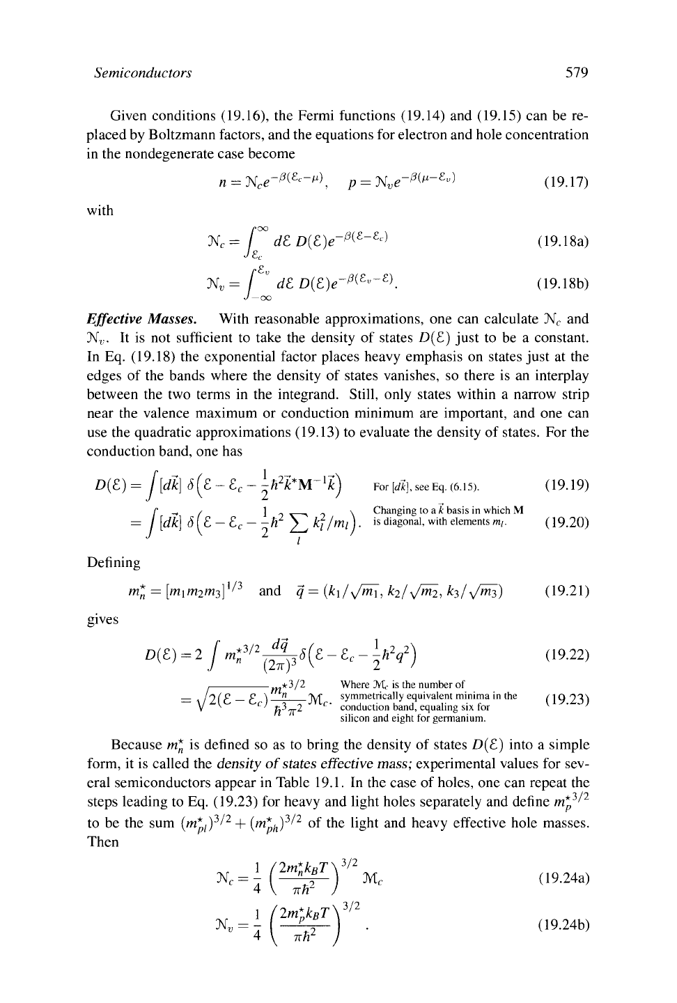
. Important features of the bands of silicon,
germanium, and gallium arsenide appear in Figure 19.8. One would expect these
materials simply to be insulators, except that the energy gap is small, on the order
of 2 eV or less. At room temperature the occupation of the conduction band is
proportional to
g
-/3£
s
/2 ^ jQ-9 For ß = \/k
B
T =40 eV"
1
and £
s
= 1 eV. The factor (19 12)
of 1/2 is a bit surprising, but will emerge from analysis. ^
Because thermal excitation provides exponentially growing numbers of mobile
charge carriers, the electrical conductivity of semiconductors grows exponentially
Figure 19.8. Essential features of band structures of silicon, germanium, and gallium
arsenide. All have band gaps on the order of
1
eV. The bottom of
the
conduction band for
silicon and germanium does not lie at T, so these materials have an indirect
gap.
Gallium
arsenide, by contrast, has a direct gap. These diagrams are extracted from Figures 23.15
and 23.16, which contain information on how they were obtained.
576
Chapter 19. Electronics
with temperature, in contrast with metals where scattering generally reduces con-
ductivity as temperature goes up. As the band gap £
g
sinks below
1
eV, thermal ex-
citation becomes a sufficiently important source of carriers that the semiconductors
conduct at room temperature. More important is the fact that the electrical prop-
erties of semiconductors are enormously sensitive to the presence of certain types
of impurities, which make their presence felt even at concentrations on the order
of one part in 10
10
. Before the role of impurities was understood, semiconductors
seemed capricious and unreliable. Now that they are not only understood but can
be controlled, the impurities are employed to give semiconductors tremendously
interesting and variable electrical transport properties, with which the electronics
industry has developed and grown for over four decades. The word "impurity"
connotes something undesirable, so one stops using it in reference to elements in-
tentionally added to semiconductors and refers to "dopants" and "doping" instead.
Band Structure of
Semiconductors.
Because of the great importance of the en-
ergy gap in semiconductors, a few words are in order on how it is measured and
calculated. In fact, neither experimental measurement nor theoretical calculation is
straightforward. The most precise experimental technique is optical absorption.
According to a simple band-theory picture, light falling upon a semiconductor
should pass through unimpeded until the energy of a photon is adequate to cre-
ate an excitation of energy
8.
g
,
after which absorption should rapidly increase. The
actual story of what happens in such experiments is sufficiently complex and in-
teresting that it is deferred to Chapters 21 and 22. Some of the effects should,
however, be mentioned now.
1.
Any transition involving a photon must conserve not only energy but also mo-
mentum. The momentum carried by a photon turns out to be negligible com-
pared with that of typical electron states. In Figure 19.8, the lowest-energy
spot in the conduction band of silicon lies at about 8/10 of the way toward X,
while the highest-energy spot in the valence band lies at T. An electron oc-
cupying a state near X cannot transfer to T simply by emitting a photon. The
transition is therefore comparatively rare, with phonons supplying the missing
momentum. For this reason, silicon is called an indirect semiconductor, as it
has an indirect gap. Germanium is also an indirect semiconductor, and the
bottom of its conduction band lies at L. Many optical applications demand
a direct semiconductor, where the lowest point of the conduction band lies
directly above the highest point of the valence band. For these applications,
GaAs is the most important material.
2.
Near the band edge, where optical absorption is supposed to vanish, it usually
displays one or more thin sharp peaks. These peaks are signatures of excitons,
which are bound electron-hole pairs whose energy can sit slightly below any
states describable in the one-electron picture.
3.
Photons whose energy lies below the band gap and out of range of excitons
continue to be absorbed, at a rate that decreases exponentially the farther they
lie below the band edge. This absorption is due to impurities and fluctuations.
Semiconductors
577
Table 19.1. Semiconductor data
Com-
£g
d£,
g
/dT nje°
m*
n
m^
n?
pl
JL,, Ji
p
pound
(eV)
(eV/K) (cirr
3
)
(m) (m) (m)
(cm
2
/V
s) (
cm
2
/V
s)
Si
Ge
GaAs
SiC
AlAs
AlSb
GaN
GaSb
InP
InAs
InSb
i
i
d
i
i
i
d
d
d
d
d
1.11
0.74
1.43
2.2
2.14
1.63
3.44
0.7
1.34
0.36
0.18
-9.0
-3.7
-3.9
-5.8
-4
-4
-6.7
-3.7
-2.9
-3.5
-2.8
10"
5
io-
4
IO"
4
10"
4
IO"
4
IO"
4
io-
4
IO"
4
IO"
4
io-
4
IO"
4
1.02
IO
10
2.33-IO
13
2-10
6
2-10
17
2-10
17
IO
14
1.2-10
s
1.3- IO
15
2.0-IO
16
11.9
16.5
12.5
9.7
10.0
12.0
12.0
15.7
15.2
15.2
16.8
1.18
0.55
0.067
0.82
0.5
0.3
0.3
0.05
0.073
0.027
0.013
0.54
0.3
0.50
1
0.5
1
1
0.3
0.6
0.4
0.4
0.15
0.04
0.07
0.26
0.5
0.04
0.12
0.03
0.02
1350
3900
7900
900
294
200
440
7700
5400
30
000
77
000
480
1800
450
50
400
1600
150
450
850
Data
on
whether
a
compound has
a
direct (d)
or
indirect (i) gap, energy gap, static dielectric
constant, effective masses,
and
mobilities,
for
some semiconductors.
The
electron effective
massm*
is the
density
of
states effective mass defined
in
Eq. (19.23). The data refer
to
room
temperature,
and to
samples with donor
and
acceptor impurities
at
densities
of
IO
15
cm
-3
or less. Source: Landolt
and
Bernstein (New Series) vol.
17 and
Pierret (1996).
Despite these experimental complications
the
experimental determination
of
band gaps
can be
made rather precisely.
Not
only
the
energy
gap, but
also
the
structure
of the
energy bands
in the
neighborhood
of
valence band maxima
and
conduction band minima,
is
important.
One can fit the
energy
to a
quadratic form
and write
H
2
^
_ -
P-
— P -I yfc*M k For electrons in the conduction band. ( \Q 13a)
k
c
2 "
h
2
~
£- = £„
k*M~
]
k,
For holes in the valence band. (19.13b)
where
M is the
effective mass tensor.
For
silicon, germanium,
and
gallium
ar-
senide,
the
bands
at the
valence maximum would
be
threefold degenerate
in the
absence
of
spin.
The
spin-orbit interaction splits
off one of the
bands, leaving
two above
it
that still
are
degenerate
at T. The two
bands have, however, differ-
ent curvatures near
T,
leading
to
heavy holes
(low
curvature)
and
light holes (high
curvature), both
of
which contribute
to the
transport properties
of
semiconductors.
Because
of the
great degree
of
symmetry associated with
T, the
energy surfaces
of
these holes
are
spherically symmetrical,
and the
effective mass tensors
are
multi-
ples
of the
unit matrix.
The conduction band minimum
in
gallium arsenide
is
nondegenerate
and
spher-
ical.
In
silicon
and
germanium,
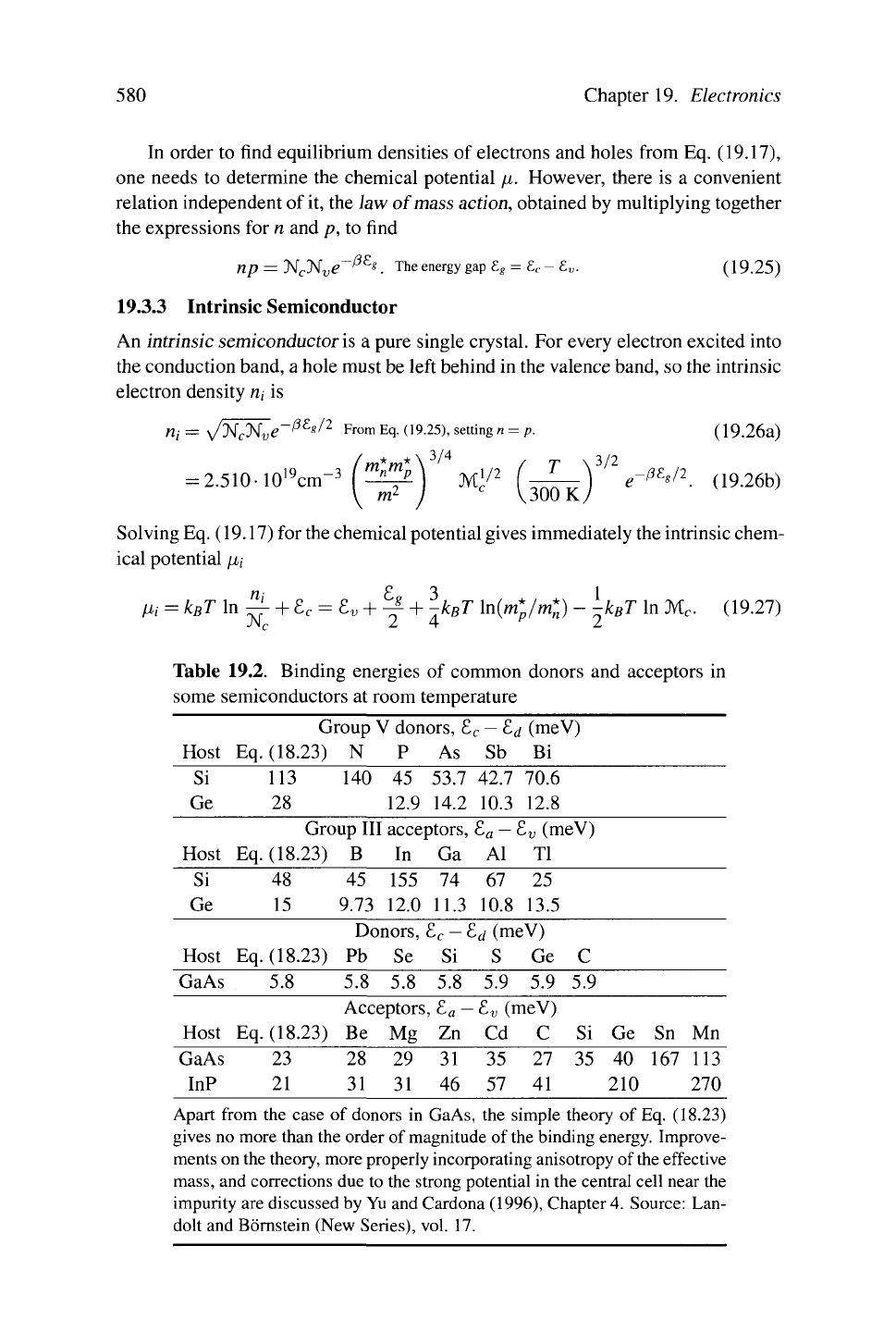
the
conduction band minima
are
quite anisotropic,
and consist
in a
number
of
symmetrically arrayed pockets
of
electrons,
as
shown
in Figure
19.9. The
effective mass tensors have been measured
by the
technique
of
cyclotron resonance,
to be
discussed
in
Section
21.2.
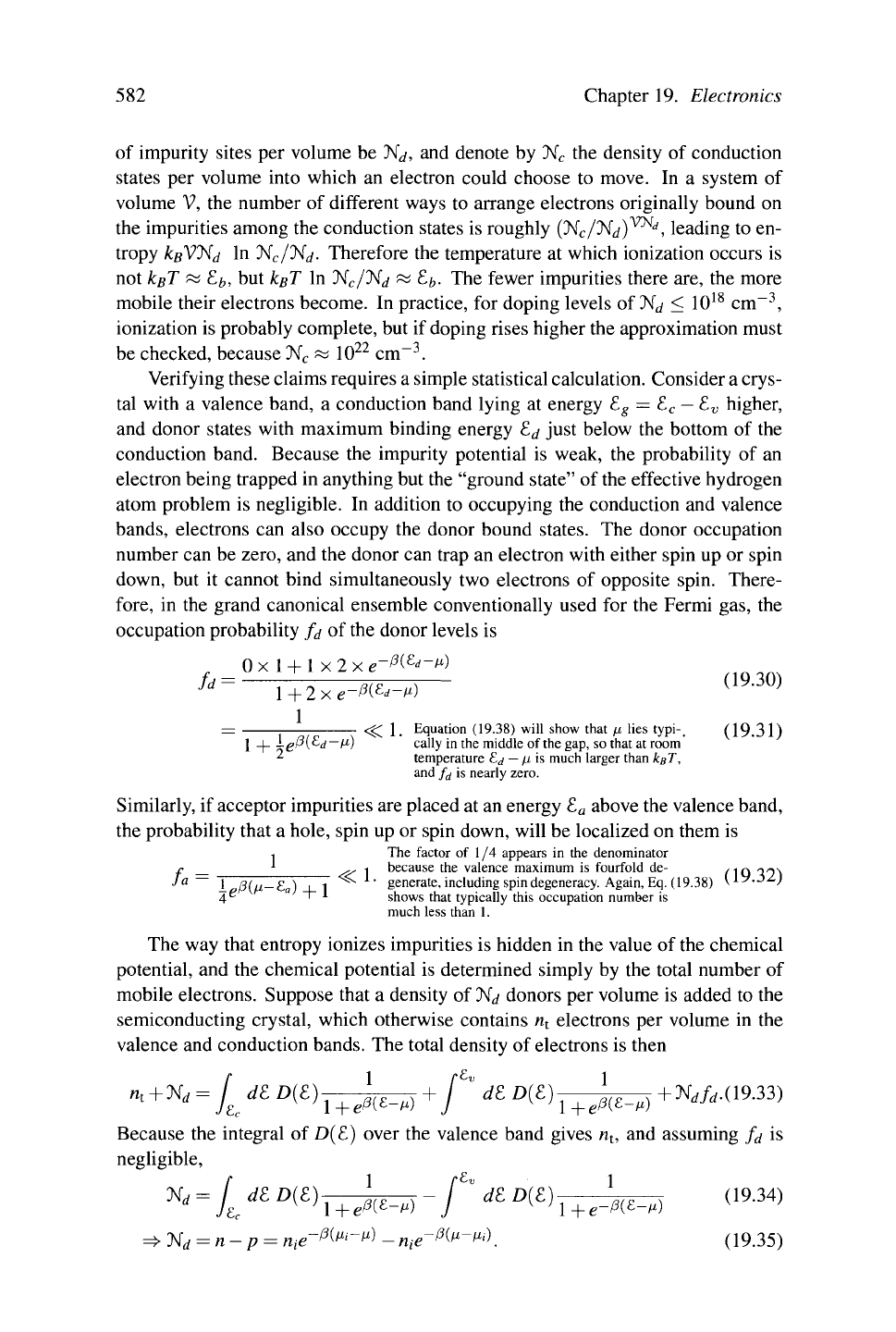
578
Chapter 19. Electronics
Figure 19.9. (A) The conduction band minima in germanium lie along (111) and strad-
dle the zone boundary, producing four inequivalent pockets of electrons with a highly
anisotropic effective mass. (B) In silicon, the conduction band minima lie 8/10 of
the
way
toward (100), producing six pockets of
electrons,
but only three with distinct symmetries.
19.3.2 Semiconductor in Equilibrium
Electron and Hole Densities. In equilibrium, the numbers of mobile charge
carriers in a semiconductor are given by the Fermi function. The volume density
of electrons n above the conduction band edge is given by
n
=
£
dem
eßV-»)
+ V
(19
-
14)
while the density of holes p below the valence band edge is
= / d£D{Z)
Nondegenerate Semiconductors. These expressions simplify for a
nondegenerate
semiconductor, which is one for which the probability of occupying states near the
band edge is exponentially small: that is,
tL
c
—
ß^>kßT
and fl — £„ 3> £g7\ A practical criterion is £
c
- ß >
3k
B
T.
(19.16)
When these conditions hold, the semiconductor is quite different from most met-
als.
Whereas in metals carrier concentrations are on the order of 10
22
electrons per
cubic centimeter, for nondegenerate semiconductors carrier concentrations are on
the order of 10
19
cm
-3
or less. Whether a semiconductor lies in the nondegener-
ate limit or not will depend upon the density of dopants (impurities) added to it.
In semiconductor devices, dopant densities are frequently great enough to cause
violation of inequalities (19.16). Nevertheless, the nondegenerate limit is of great
utility because the transport properties of semiconductor devices are largely deter-
mined by the regions with light doping, while the regions with heavy doping act
like short circuits and can often be ignored.
(19.15a)
(19.15b)
Semiconductors 579
Given conditions (19.16), the Fermi functions (19.14) and (19.15) can be re-
placed by Boltzmann factors, and the equations for electron and hole concentration
in the nondegenerate case become
n = 'N
c
e-
ß(
-
£c
-'
i
\ p = Ke-*-
£
»
)
(19.17)
with
roo
N
c
= / J£ D(£)g-^
e_£c)
(19.18a)
JE.C
K= / " rf£D(£)g-^
e
"
_e)
. (19.18b)
Effective Masses. With reasonable approximations, one can calculate N
c
and
N,
;
.
It is not sufficient to take the density of states D(£) just to be a constant.
In Eq. (19.18) the exponential factor places heavy emphasis on states just at the
edges of the bands where the density of states vanishes, so there is an interplay
between the two terms in the integrand. Still, only states within a narrow strip
near the valence maximum or conduction minimum are important, and one can
use the quadratic approximations (19.13) to evaluate the density of states. For the
conduction band, one has
D(E)= [[dk]ô(£-e.
c
-^h
2
k*M-
l
k) For[d*],seeEq.(6.i5). (19.19)
/
_ i 1 \ Changing to a k basis in which M
[dk]
8(£.-£,
c
- -h
1
^2
k
i/
m
i)•
isdia
s°
Ml
-
withelementsm
'-
(19.20)
z
Defining
(ti/^W^.Wv^J) (19.21)
gives
\h
2
q
2
) (19.22)
- k 3 /2 Where JYk is the number of
Illy,
m*
= [in
D(£)
im
2
m
3
]
-'/■
'/
3
and
m
*3/2 dq
" (2vr)
:
q=\
A
8
-
_ ./2(£ — £ ) " 1y[ symmetrically equivalent minima in the (19 23^
»
C
fr^TT^
°'
concm
ction band, equaling six for ^ ' '
silicon and eight for germanium.
Because m* is defined so as to bring the density of states D(E) into a simple
form, it is called the density of
states
effective mass; experimental values for sev-
eral semiconductors appear in Table 19.1. In the case of holes, one can repeat the
steps leading to Eq. (19.23) for heavy and light holes separately and define m*
3
'
2
to be the sum (m*,)
3
/
2
+ (w*
ft
)
3
/
2
of the light and heavy effective hole masses.
Then
^)
3
M
C
(19.24a,
nn /
2m*
p
k
B
T\
3/2
—i^-
. (19.24b)
580 Chapter 19. Electronics
In order to find equilibrium densities of electrons and holes from Eq. (19.17),
one needs to determine the chemical potential p. However, there is a convenient
relation independent of it, the law of mass action, obtained by multiplying together
the expressions for n and p, to find
np = J<
c
'N
v
e~
ßE
z. The energy gap E
g
= E
c
-E
v
. (19.25)
19.3.3 Intrinsic Semiconductor
An intrinsic semiconductor
is
a pure single crystal. For every electron excited into
the conduction band, a hole must be left behind in the valence band, so the intrinsic
electron density n, is
m = \/H^e~
ߣs/2
From Eq. (19.25), setting
n
= p. (19.26a)
mtm*
3/4
r- {^L\
m
= 2.510- 10'W(^j Mf- (^) e-W. (19.26b)
Solving
Eq.
(19.17) for the chemical potential gives immediately the intrinsic chem-
ical potential pi
lH
= k
B
Tln^ + £
c
=
8,
v
+ ^ + ^-k
B
T
ln{m*
p
/m*
n
)
-
X
-k
B
T In M
c
. (19.27)
Table 19.2. Binding energies of common donors and acceptors in
some semiconductors at room temperature
Host
Si
Ge
Host
Si
Ge
Host
GaAs
Host
GaAs
InP
Group V donors, £
c
—
£</ (meV)
Eq. (18.23) N P As Sb Bi
113 140 45 53.7 42.7 70.6
28 12.9 14.2 10.3 12.8
Group III acceptors, £
a
—
£
v
(meV)
Eq. (18.23) B In Ga Al Tl
48 45 155 74 67 25
15 9.73 12.0 11.3 10.8 13.5
Donors, £
c
—
£</
(meV)
Eq. (18.23) Pb Se Si S Ge C
5.8 5.8 5.8 5.8 5.9 5.9 5.9
Acceptors, £
fl
—
£.
v
(meV)
Eq. (18.23) Be Mg Zn Cd C Si
23 28 29 31 35 27 35
21 31 31 46 57 41
Ge Sn Mn
40 167 113
210 270
Apart from the case of donors in GaAs, the simple theory of Eq. (18.23)
gives no more than the order of magnitude of the binding energy. Improve-
ments on the theory, more properly incorporating anisotropy of the effective
mass,
and corrections due to the strong potential in the central cell near the
impurity are discussed by Yu and Cardona (1996), Chapter
4.
Source: Lan-
dolt and Börnstein (New Series), vol. 17.
Semiconductors
581
The logarithm in Eq. (19.27) is of order unity or even zero if holes and electrons
have the same effective mass, so because kßT ~ 1/40 eV at room temperature and
band gaps are around 1 eV for semiconductors, the chemical potential sits smack
in the middle of the band gap. Thus it cooperates in enforcing (19.17), making the
semiconductor as nondegenerate as possible by staying away from the band edges.
Compact Expressions. Combining Eqs. (19.26) and (19.25) puts the law of mass
action in the general compact form
np = nj (19.28)
and allows rewriting Eqs. (19.17) for electron and hole densities as
n = me-ftH-rt, p = me-^-^.
(
19.29)
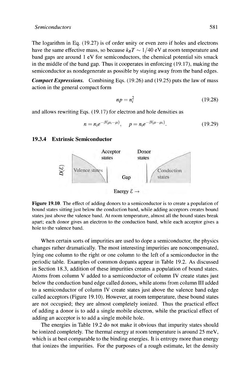
19.3.4 Extrinsic Semiconductor
Figure 19.10. The effect of adding donors to a semiconductor is to create a population of
bound states sitting just below the conduction band, while adding acceptors creates bound
states just above the valence band. At room temperature, almost all the bound states break
apart; each donor gives an electron to the conduction band, while each acceptor gives a
hole to the valence band.
When certain sorts of impurities are used to dope a semiconductor, the physics
changes rather dramatically. The most interesting impurities are noncompensated,
lying one column to the right or one column to the left of a semiconductor in the
periodic table. Examples of common dopants appear in Table 19.2. As discussed
in Section 18.3, addition of these impurities creates a population of bound states.
Atoms from column V added to a semiconductor of column IV create states just
below the conduction band edge called donors, while atoms from column III added
to a semiconductor of column IV create states just above the valence band edge
called acceptors (Figure 19.10). However, at room temperature, these bound states
are not occupied; they are almost completely ionized. Thus the practical effect
of adding a donor is to add a single mobile electron, while the practical effect of
adding an acceptor is to add a single mobile hole.
The energies in Table 19.2 do not make it obvious that impurity states should
be ionized completely. The thermal energy at room temperature is around 25 meV,
which is at best comparable to the binding energies. It is entropy more than energy
that ionizes the impurities. For the purposes of a rough estimate, let the density
582
Chapter 19. Electronics
of impurity sites per volume be N^, and denote by N
c
the density of conduction
states per volume into which an electron could choose to move. In a system of
volume V, the number of different ways to arrange electrons originally bound on
the impurities among the conduction states is roug hly (Nc/Nd)'™', leading to en-
tropy kßVJJd In
N
c
/Nj.
Therefore the temperature at which ionization occurs is
not kgT
K,
£
è
, but kßT In N
c
/Nj « £
è
. The fewer impurities there are, the more
mobile their electrons become. In practice, for doping levels of lid < 10
18
cm
-3
,
ionization is probably complete, but if doping rises higher the approximation must
be checked, because H
c
« 10
22
cm
-3
.
Verifying these claims requires a simple statistical calculation. Consider a crys-
tal with a valence band, a conduction band lying at energy £
g
= £
c
—
£„ higher,
and donor states with maximum binding energy £j just below the bottom of the
conduction band. Because the impurity potential is weak, the probability of an
electron being trapped in anything but the "ground state" of the effective hydrogen
atom problem is negligible. In addition to occupying the conduction and valence
bands,
electrons can also occupy the donor bound states. The donor occupation
number can be zero, and the donor can trap an electron with either spin up or spin
down, but it cannot bind simultaneously two electrons of opposite spin. There-
fore,
in the grand canonical ensemble conventionally used for the Fermi gas, the
occupation probability fd of the donor levels is
0 x
1
+
1
x 2 x e-P^-ti
h=
1+
2x.-^>
(1930)
<^ 1. Equation (19.38) will show that fi lies typi-. (19.31)
1 -)- ±gß{£-d—t
J
') cally in the middle of the gap, so that at room
2 temperature Ej
—
ß is much larger than kgT,
and /rf is nearly zero.
Similarly, if acceptor impurities are placed at an energy £
a
above the valence band,
the probability that a hole, spin up or spin down, will be localized on them is
. The factor of 1/4 appears in the denominator
r L „ I because the valence maximum is fourfold de- ,.,Q
Q~N
J
a
\_ 3(u—£
a
)\-\ ^ generate, including spin degeneracy. Again, Eq. (19.38) l.'■"•-JA)
4^
' * shows that typically this occupation number is
much less than 1.
The way that entropy ionizes impurities is hidden in the value of the chemical
potential, and the chemical potential is determined simply by the total number of
mobile electrons. Suppose that a density of Nd donors per volume is added to the
semiconducting crystal, which otherwise contains n
t
electrons per volume in the
valence and conduction bands. The total density of electrons is then
*
+
N'
=
J
Ec
dg
D
(
£
) i + J(e-„)
+
f
V
^
D
^
i +
J(£-M)
+Kdfä.(l933)
Because the integral of D(£) over the valence band gives n
t
, and assuming fd is
negligible,
W,
= £ dt
D^)—^-^
J£
D(E)
i+
J
ß{e
_
ß)
(19.34)
=>
N
d
= n - p = nte-P^'-A - n^^^. (19.35)