Marder M.P. Condensed Matter Physics
Подождите немного. Документ загружается.

Diodes and Transistors
593
A quasi-neutral «-doped region where the electric field is extremely small and
the density of mobile electrons is close to Nj.
A depletion region where the electric field rises rapidly to large values and where
consequently the concentrations of charge carriers rapidly fall below their val-
ues in homogeneously doped samples. In the midst of this depletion region,
the doping changes from n to p type.
A quasi-neutral p-doped region where the electric field drops back to zero and
the density of mobile holes is close to Ji
a
.
The vast majority of mobile charge carriers in the quasi-neutral n-doped region
are electrons. However, there is also a small population of holes. Similarly there
is a small population of electrons in the p-doped region. These two populations
are called minority carriers, and the operation of the diode can be understood by
carefully analyzing their behavior, because whichever of them is least mobile con-
stitutes the main bottleneck restraining charge flow through the diode.
Further progress rests upon two simplifications:
1.
The boundary between the depletion region and the quasi-neutral regions is
sharp.
In the quasi-neutral regions, the electric field is very small, and the drift
currents ep„nE (p-region) and e\i
p
pE of the minority carriers are negligible.
That is, in regions where carriers are unlikely, they obey the purely linear
equations
Jn 6Un"-
Electrons, specializing to one dimension; the
v
' "• '
""■>
prime means spatial derivative.
j
p
= -eT>
p
pf
Holes
. (19.70b)
This approximation is excellent.
2.
Recombination and generation of charge carriers is neglected in the depletion
region. This assumption is made for mathematical convenience only. The
faster the charges sweep through the depletion region, the more appropriate it
will be, but for low current flow it leads to appreciable deviation from experi-
ment.
Solution in Depletion Region. The value of the second assumption lies in the
fact that it makes possible an analytical relation for n and p in the depletion re-
gion, allowing the behavior of the diode to be obtained in closed form. Because
recombination and generation are neglected, the currents of electrons and holes are
separately conserved, and both j
n
and j
p
are constant in space. Using Eqs. (19.67),
one can quickly find a solution for n and p which according to Problem 4 is
n(jt)=V
[VW_V(
*
)1
\ + -£- /
dx
>
e
-ße[V(x>)-V
{x
„)]
e^d^n Jx„
-
jp
r
dx'
e
ße[v(x')-v(
X
„)}
eX
a
V
p
(19.71a)
.(19.71b)
594 Chapter 19. Electronics
Under equilibrium conditions, where no current flows, the second terms on the
right-hand side of Eqs. (19.71) vanish. Ignoring this second term is very conve-
nient, because use of the first term requires only knowledge of the total change in
potential across the depletion region, while the second would require knowledge of
details of
the
profile of V
(x).
Fortunately, for most cases of interest the second term
remains negligible relative to the first, even out of equilibrium. Looking ahead to
Eq. (19.77), one can estimate its size in the presence of applied voltage
VA
to be
2
_
'
—
-
e
0eVA
Ki
lO~
lO
e
0eVA
. Junction widths are typically 10
2
times smaller (19.72)
KaJNfrf
L
n
than diffusion lengths, and n
2
/^^
~
10
-8
.
Therefore, Eq. (19.71) can be replaced by the law of the junction:
n{x)
=
N
de
ße[v(x)-v(x
n
)]
(19.73a)
p{x) =
J{
a
e~M
v
W-
v
(
x
^
(19.73b)
2 SeeEq. (19.49), and use
=>
n
(x
D
) =
N
d
e
0e[VA
~
V
^
=
^e
ßeVA
«yPn»imation Eq. (19.40). Note
(19J3
C
)
v
>'
!
" yj
that the density ot minority earners
v
'
a
on the left side of the junction is
being set by the density
DM^
of
donors on the right side.
„2
p(x
n
) =
■Xaef'W*-^
= ^-e
ßeVA
. (19.73d)
Solution in Quasi-Neutral Region. Equations (19.73) constitute a complete so-
lution for the charge carriers in the depletion region. They cannot be used alone
to find the current flowing through the diode, because Eqs. (19.73) produce a com-
plete cancellation of diffusion and drift currents, and putting back in the tiny cor-
rections of Eqs. (19.71) to obtain nonzero current means adding back in terms
proportional to
j
n
and
j
p
which are still unknown. In this sense, Eqs. (19.73) are
compatible with
a
huge range of currents through the diode. However, by using
Eqs.
(19.73) to impose a boundary condition upon the solutions of Eqs. (19.68),
the currents are rapidly determined.
Using the expressions for current (19.70) in Eqs. (19.68) gives in steady state
J2
n n
„(o)
Applies only to minority carriers, and
Q
=
2)
£_ £_ £_
only in quasi-neutral regions.
p
m
and (19.74a)
dx
T
p
«
(0
' are the equilibrium minority
carrier densities, given by Eqs. (19.39)
or (19.40).
£■„
n
_
„(0)
Q
= tD
än_n_J}_
(19
.
74b)
dx
A
T
n
which have solution
p—
n(°'
=
\p(x
n
) — n^]g~y
x
~
x
")/ P Applies where p is the minority carrier, to the (19.75a)
right of
x„.
fl — fj(°)
=
IW;t
n
) — n'
0
'le'
X—Xp
''
"
Applies where « is the minority carrier, to the (J9 75b)
1
v p
' '
left of
x
p
.
v
' '
where
Ln =
V^Tn and
L
P
=
JV
P
T
P
(19.76)
Diodes and Transistors
595
are the diffusion lengths
of
electrons
in
the /j-doped region, and
of
holes
in
the
«-doped region, respectively. The currents due to these minority carriers are, from
Eqs.
(19.67),
T>
j
n
=e—[n(x
p
)-n
i0)
]
Evaluate Eq. (19.75a) at x„. (19.77a)
L
n
T>
n
2
=
e
——!-\
e
ß
eV
A-\}
Use Eqs. (19.73c) and (19.40b).
(19
77b)
L„ JS
a
j
p
= e^[p(x
n
)-p
w
}, (19.77c)
T>
n
2
=
e
—E. _!_
\ßf
ieVA
-
1
], Use Eqs. (19.73d) and (19.39b).
(19.77d)
L
p
N
rf
producing a total current per volume given by the ideal diode or Shockley equation,
j = en][e^-\]
T>„
D
r
L
n
Ji
a
L
d
N
d
Doping must be heavy enough (19
78)
that Eqs. (19.39) and (19.40)
hold.
One of the most important features of
Eq.
(19.78) is that because N
a
ar
>d
N</
appear
in denominators, current flow
is
set by the side
of
the diode that
is
most lightly
doped. The heavily doped side acts like
a
short circuit. This fact is particularly
important for the design of the transistor.
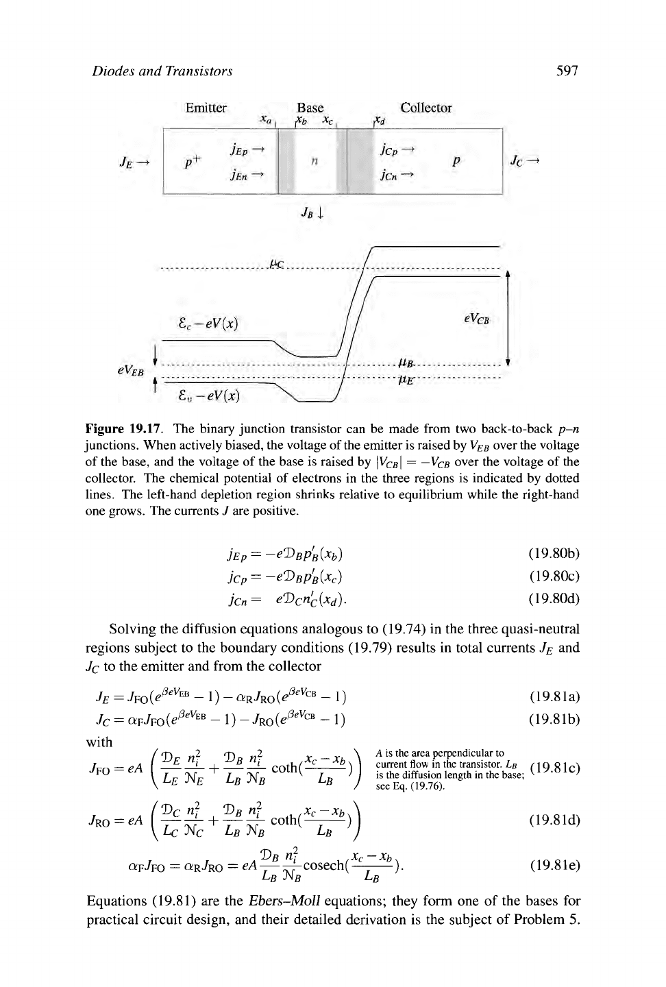
19.4.5 Transistor
By the 1920s numerous scientists realized that because electronics was based upon
the diode and the triode, and because semiconductor diodes could be created (al-
though unreliably),
it
would be valuable to create
a
semiconductor analog
of
the
triode. Twenty-five years elapsed between the first ideas, and the first practical
implementation, called the transistor by Bardeen and Brattain (1948).
The
first
working transistor involved contact between thin metal whiskers and semiconduc-
tors,
rather like the Schottky diodes. It was unable to carry large currents and never
developed into
a
commercial device, but the research project in which the point-
contact transistor was created uncovered much of the basic physics of semiconduc-
tor
junctions,
particularly the fact that transport in diodes is dominated by minority
carriers. The bipolar junction
transistor
followed not longer after and served as the
foundation for the first developments of semiconductor electronics.
The basic idea
of
the bipolar junction transistor
is to
take advantage
of
the
large disparity between electron and hole currents
in a
diode where one side
is
much more heavily doped than the other. Consider, for example,
a
p
+
n junction,
where the superscript
+
indicates heavy doping, on the order
of
10
18
cm
-3
,
so
that the assumption the semiconductor is nondegenerate breaks down. For steady
current flow under forward bias, a tiny electron current flows into the n region, and
a large hole current flows in to the
p
+
region. In a diode, the hole current would be
drawn to the
n
region and out of the semiconductor, but in the transistor the hole
596
Chapter 19. Electronics
current is diverted by making the n region much narrower than the diffusion length
L
p
of the minority carriers and placing it in contact with a second pn junction,
which is under reverse bias. The reverse bias means that in the depletion region
electric fields propel holes toward the p region and repel electrons. Whenever a
hole diffusing about in the n region wanders into this second depletion region,
it is trapped and sent off to the collector. The net effect is to split the current
traveling into the emitter into its constituent components, with almost all the holes
going out the collector and almost all the electrons coming in from the base. The
large ratio between these two currents, along with the fact that they are linearly
related according to Eqs. (19.77), means that the transistor can function as a linear
amplifier. On the other hand, if the current to the base is reversed, the current out
the collector does not follow it linearly but drops to very low values. Thus the
transistor also rectifies current and can be used as a binary switch.
The mathematical analysis of
the
binary junction transistor involves no ideas or
assumptions not already present in the case of the ideal diode. The only difficulty
is that there is now a large number of different regions, so the notation becomes
confusing. Once again the basic idea is to assume steady-state conditions and
1.
Separate the device into quasi-neutral and depletion regions.
2.
Ignore recombination-generation in depletion regions.
Also as before, the strategy is to focus upon the minority carriers in each region.
The fields that need to be found are
HE{X), the electron concentration in the emitter,
PB(X),
the hole concentration in the base, and nc(x), the electron concentration in
the collector, regions labeled in Figure 19.17.
The concentrations of the minority carriers at the edges of each depletion re-
gion are determined by precisely the considerations that produced the ideal diode
equation. So, in analogy with Eqs. (19.73c) and (19.73d),
J4E
is the acceptor concentration in the emit- ( 19.79a)
ter
region,
VEB
> 0 (for active bias) is the
voltage
of emitter over
base.
n
E
{x
a
) =
Pn{xb) =
PB{X
C
) =
nc{xd) =
.
H
i JieVEB
"N
£
f7
2
. "■'
e
ßeV
EB
"N
ß
.
n
i
p
ßeVcB
"N/
.
n
i
p
ßeVcB
"Ne
~HB
is the donor
concentration
in the base
region.
( 19.79b)
VÇB
< 0 (for active bias) is the voltage of (19.79c)
the
collector relative to the
base;
when
VQB
is
negative,
collector voltage is below
base.
"HQ
is the acceptor concentration in the col- (19.79d)
lector
region.
These boundary equations are coupled to the diffusion equations in the three quasi-
neutral regions, which are unchanged from Eqs. (19.70). The currents of electrons
and holes in the emitter and collector can then be calculated from
j
En
=
eD
E
ri
E
(x
a
)
(19.80a)
Diodes and Transistors
597
Figure 19.17. The binary junction transistor can be made from two back-to-back p-n
junctions. When actively biased, the voltage of
the
emitter is raised by
VEB
over the voltage
of the base, and the voltage of the base is raised by \VQB\ = —VCB over the voltage of the
collector. The chemical potential of electrons in the three regions is indicated by dotted
lines.
The left-hand depletion region shrinks relative to equilibrium while the right-hand
one grows. The currents J are positive.
JE
P
= -eT>
B
p'
B
(x
b
) (19.80b)
j
Cp
= -eV
B
p'
B
(x
c
) (19.80c)
j
Cn
=
eV
c
n'
c
(x
d
). (19.80d)
Solving the diffusion equations analogous to (19.74) in the three quasi-neutral
regions subject to the boundary conditions (19.79) results in total currents JE and
Jc to the emitter and from the collector
JE
= JFo(e
ßeVEB
- 1) - a
R
J
RO
(e
0eVc
» - 1) (19.81a)
Jc = a
¥
J
FO
(e
ßeVEB
~ l)-J
RO
(e
ßeVcB
- 1) (19.81b)
with
(
T)r n
2
T)D M
2
v _
r
, \ A is the area perpendicular to
—-£-
+—-f coth(^—^)
cu
";
en
'.fl
owin
**T
si
T'
h
LB
(
19
-
81c
)
T
T,
TvJV T „ T\[„
v
T r, ' I is the diffusion length in the base;
v
'
L.E
JN£ L
B
J\
B
L
B
J
seeEq(1976)
/ A (^cn
2
T>
B
n
2
t
,,Xc-x
b
\ ,.„„.,
J
KO =
eA\-——
+
——colh(—
) (19.81d)
\^ Lc N
c
L
B
JJ
B
L
B
J
a
F
J
FO
=
ÖR^RO
= M —-j-cosech(-^- ). (19.81e)
L
B
N
B
L
B
'
Equations (19.81) are the Ebers-MoU equations; they form one of the bases for
practical circuit design, and their detailed derivation is the subject of Problem 5.
598
Chapter 19. Electronics
Note that the diffusion length of the base LB must be comparable to or greater than
x
c
—Xb,or else control of the collector current by the base is lost.
19.5 Inversion Layers
19.5.1 Heterostructures
The earliest electronic devices depended upon the contact between metal and vac-
uum, the next generation depended upon contact between metal and semiconduc-
tor, and the next industry depended upon junctions between regions of different
doping, as well as junctions between semiconductors and insulators. A new gen-
eration of semiconductor devices is now evolving that depends upon junctions be-
tween different semiconductor alloys. The advantage of these is that they make
possible the creation of heterostructures where the band gap varies in ways that
would never occur spontaneously in nature.
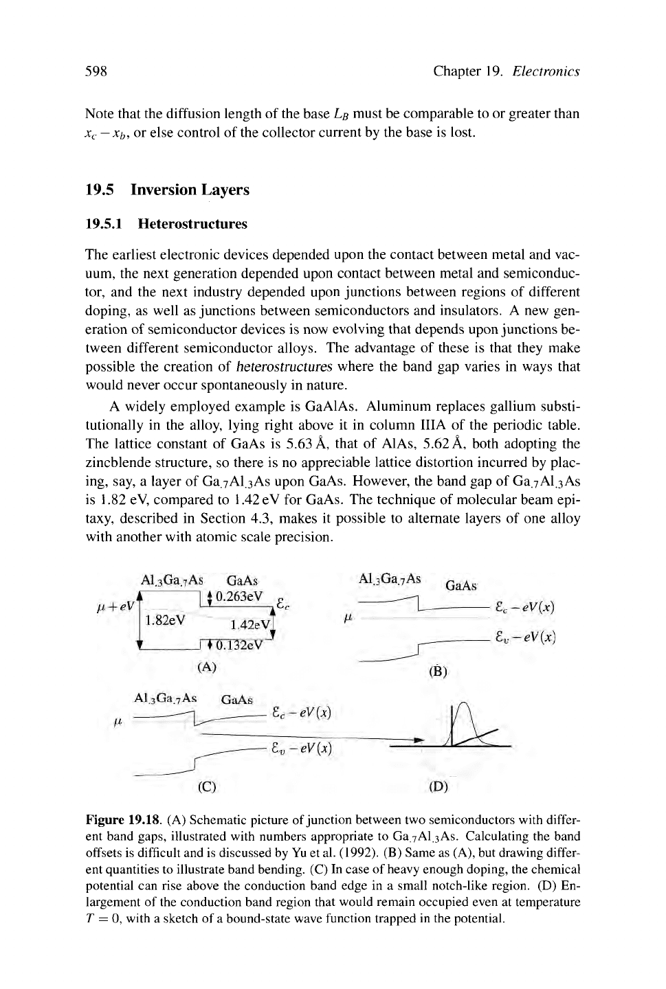
A widely employed example is GaAlAs. Aluminum replaces gallium substi-
tutionally in the alloy, lying right above it in column IIIA of the periodic table.
The lattice constant of GaAs is 5.63 Â, that of AlAs, 5.62 Â, both adopting the
zincblende structure, so there is no appreciable lattice distortion incurred by plac-
ing, say, a layer of Ga.7Al.3As upon GaAs. However, the band gap of Ga.7Al.3As
is 1.82 eV, compared to 1.42 eV for GaAs. The technique of molecular beam epi-
taxy, described in Section 4.3, makes it possible to alternate layers of one alloy
with another with atomic scale precision.
Figure 19.18. (A) Schematic picture of junction between two semiconductors with differ-
ent band gaps, illustrated with numbers appropriate to Ga.7Al.3As. Calculating the band
offsets is difficult and is discussed by Yu et
al.
(1992). (B) Same as (A), but drawing differ-
ent quantities to illustrate band bending. (C) In case of heavy enough doping, the chemical
potential can rise above the conduction band edge in a small notch-like region. (D) En-
largement of the conduction band region that would remain occupied even at temperature
T = 0, with a sketch of a bound-state wave function trapped in the potential.
Inversion Layers
599
The formulas describing the profiles of charge around heterostructure junctions
are not dramatically different from those of Section 19.4.2, and the main physical
results can be deduced from diagrams in the spirit of Figs. 19.11 and 19.14, as
displayed in Figure 19.18. The electron bands are discontinuous in the vicinity of
the junction, which permits some interesting possibilities. A notch in the bands,
such as shown in Figure 19.18(C), creates a small region that is occupied even at
zero temperature, called an inversion layer.
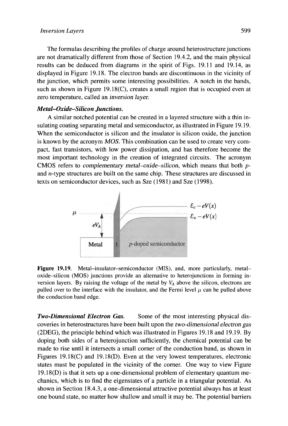
Metal-Oxide-Silicon Junctions.
A similar notched potential can be created in a layered structure with a thin in-
sulating coating separating metal and semiconductor, as illustrated in Figure 19.19.
When the semiconductor is silicon and the insulator is silicon oxide, the junction
is known by the acronym MOS. This combination can be used to create very com-
pact, fast transistors, with low power dissipation, and has therefore become the
most important technology in the creation of integrated circuits. The acronym
CMOS refers to complementary metal-oxide-silicon, which means that both p-
and n-type structures are built on the same chip. These structures are discussed in
texts on semiconductor devices, such as Sze (1981) and Sze (1998).
Figure 19.19. Metal-insulator-semiconductor (MIS), and, more particularly, metal-
oxide-silicon (MOS) junctions provide an alternative to heterojunctions in forming in-
version layers. By raising the voltage of the metal by
VA
above the silicon, electrons are
pulled over to the interface with the insulator, and the Fermi level /x can be pulled above
the conduction band edge.
Two-Dimensional Electron Gas. Some of the most interesting physical dis-
coveries in heterostructures have been built upon the two-dimensional
electron
gas
(2DEG), the principle behind which was illustrated in Figures 19.18 and 19.19. By
doping both sides of a heteroj unction sufficiently, the chemical potential can be
made to rise until it intersects a small corner of the conduction band, as shown in
Figures 19.18(C) and 19.18(D). Even at the very lowest temperatures, electronic
states must be populated in the vicinity of the corner. One way to view Figure
19.18(D) is that it sets up a one-dimensional problem of elementary quantum me-
chanics, which is to find the eigenstates of a particle in a triangular potential. As
shown in Section
18.4.3,
a one-dimensional attractive potential always has at least
one bound state, no matter how shallow and small it may be. The potential barriers
600 Chapter 19. Electronics
in the vicinity of the heterojunction are on the order of 0.1 eV. At room tempera-
ture,
electrons would escape the restraining potential, and in fact the region to the
right of the junction in Figure 19.18 would constitute an «-doped semiconductor in
the degenerate limit. However, at temperatures of a few kelvin or less where ex-
periments are characteristically performed, only the ground state has measurable
occupation. This restriction to low temperatures is clearly a disadvantage. To over-
come this restriction, it is not sufficient to find materials so that the energy scale of
Figure 19.18 is multiplied by 100. The great mobility of electrons at low tempera-
tures and the great purity achievable in semiconductors are equally important.
Figure 19.18 may lead to a mental picture in which electrons are trapped in one-
dimensional potentials. The trapping is only in the z direction, as shown in Figure
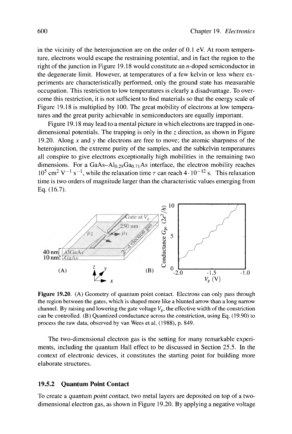
19.20.
Along x and y the electrons are free to move; the atomic sharpness of the
heterojunction, the extreme purity of the samples, and the subkelvin temperatures
all conspire to give electrons exceptionally high mobilities in the remaining two
dimensions. For a GaAs-Alo.29Gao.71 As interface, the electron mobility reaches
10
5
cm
2
V
-1
s
_1
, while the relaxation time r can reach 4• 10~
12
s. This relaxation
time is two orders of magnitude larger than the characteristic values emerging from
Eq. (16.7).
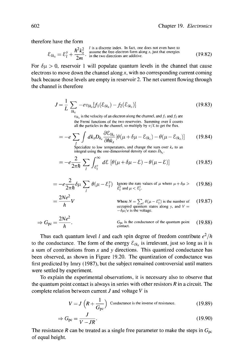
10
(A)
k:
(B)
u
G
e3
T3
C
O
U
5 -
-2.0
Figure 19.20. (A) Geometry of quantum point contact. Electrons can only pass through
the region between the gates, which is shaped more like a blunted arrow than a long narrow
channel. By raising and lowering the gate voltage V
g
, the effective width of
the
constriction
can be controlled. (B) Quantized conductance across the constriction, using Eq. (19.90) to
process the raw data, observed by van Wees et al. (1988), p. 849.
The two-dimensional electron gas is the setting for many remarkable experi-
ments, including the quantum Hall effect to be discussed in Section 25.5. In the
context of electronic devices, it constitutes the starting point for building more
elaborate structures.
19.5.2 Quantum Point Contact
To create a quantum point contact, two metal layers are deposited on top of a two-
dimensional electron gas, as shown in Figure 19.20. By applying a negative voltage
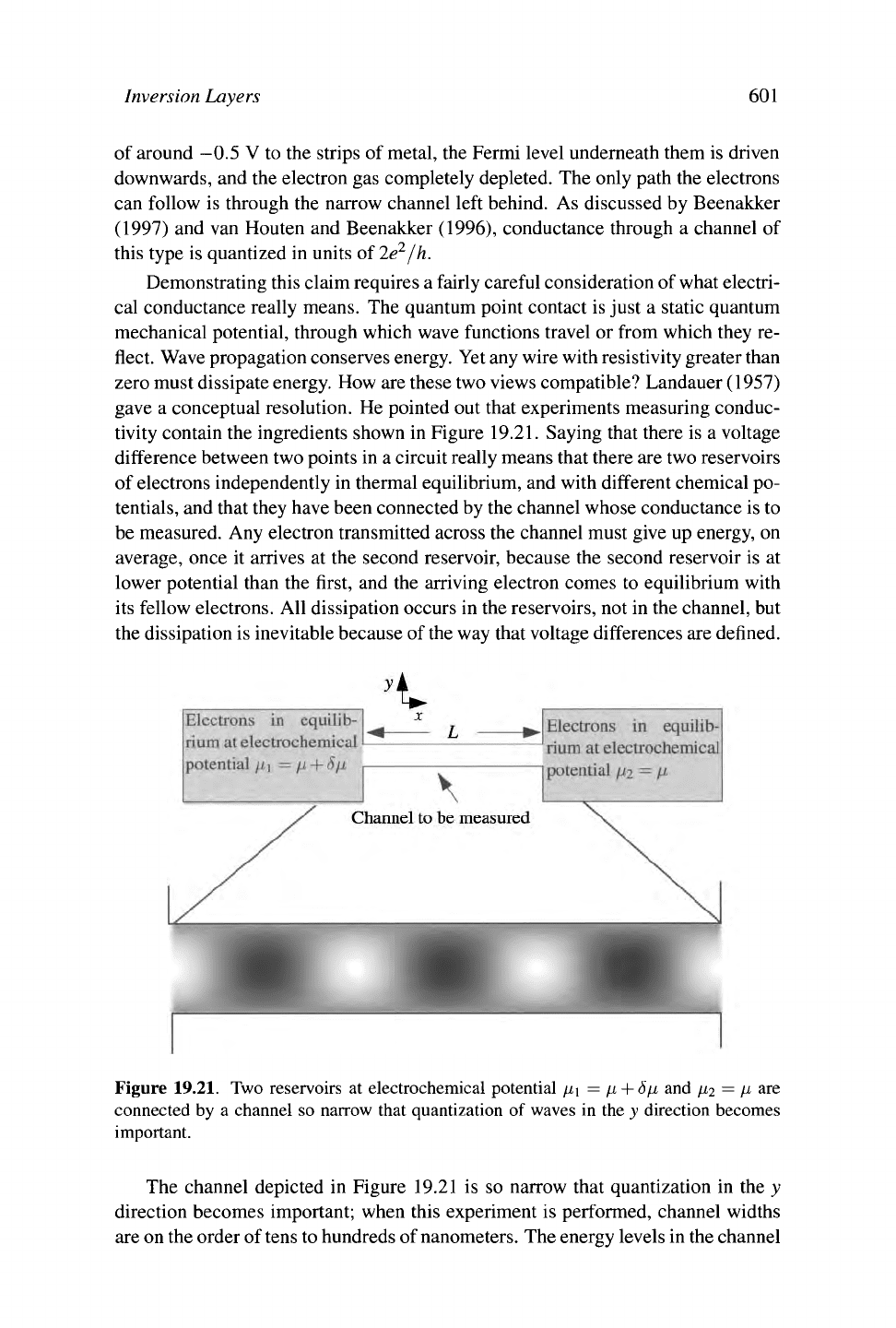
Inversion Layers
601
of around —0.5 V to the strips of metal, the Fermi level underneath them is driven
downwards, and the electron gas completely depleted. The only path the electrons
can follow is through the narrow channel left behind. As discussed by Beenakker
(1997) and van Houten and Beenakker (1996), conductance through a channel of
this type is quantized in units of 2e
2
/h.
Demonstrating this claim requires a fairly careful consideration of what electri-
cal conductance really means. The quantum point contact is just a static quantum
mechanical potential, through which wave functions travel or from which they re-
flect. Wave propagation conserves energy. Yet any wire with resistivity greater than
zero must dissipate energy. How are these two views compatible? Landauer (1957)
gave a conceptual resolution. He pointed out that experiments measuring conduc-
tivity contain the ingredients shown in Figure
19.21.
Saying that there is a voltage
difference between two points in a circuit really means that there are two reservoirs
of electrons independently in thermal equilibrium, and with different chemical po-
tentials, and that they have been connected by the channel whose conductance is to
be measured. Any electron transmitted across the channel must give up energy, on
average, once it arrives at the second reservoir, because the second reservoir is at
lower potential than the first, and the arriving electron comes to equilibrium with
its fellow electrons. All dissipation occurs in the reservoirs, not in the channel, but
the dissipation is inevitable because of
the
way that voltage differences are defined.
Figure
19.21.
Two reservoirs at electrochemical potential /xi = ß + 5ß and ß2 = ß are
connected by a channel so narrow that quantization of waves in the y direction becomes
important.
The channel depicted in Figure 19.21 is so narrow that quantization in the y
direction becomes important; when this experiment is performed, channel widths
are on the order of
tens
to hundreds of
nanometers.
The energy levels in the channel
602
Chapter 19. Electronics
therefore have
the
form
f-2j2
' '
s a
discrete index. In fact, one does not even have to
P cy _i_ x assume the free-electron form along x, just that energies ('10 89^
t'lkx ^l H ^ • in the two directions are additive.
1.
' "•°A)
For 5ji > 0, reservoir 1 will populate quantum levels in the channel that cause
electrons to move down the channel along x, with no corresponding current coming
back because those levels are empty in reservoir
2.
The net current flowing through
the channel is therefore
J= 7 E -^/Ü/i(£/Ü -/2(£*ü] (19.83)
L
Ik,
vik
x
is the velocity of an electron along the channel, and /] and fi are
the Fermi functions of the two reservoirs. Summing over k counts
all the particles in the channel, so multiply by v/L to get the flux.
Jdk
x
D
kx
^[O(ii + 6ii-£.
lkll
)-0(tJL-£
lkx
)] (19.84)
/
Specialize to low temperatures, and change the sum over k
x
to an
integral using the one-dimensional density of states D^.
2
2TTH
POO
y dl
[e{fi
+ Sfi-E)-6(fi-E)]
(19.85)
, Je:
2
—e
Ou y^ 9(u
—
£?)
I
g
nore
the rare values of
ß
where
H
+
S/J,>
(19.86)
2-Kh ^ ^ ^
U
£>'and
Ai
<£;.
2Ne
2
V Where N = J]
;
9(p - £j) is the number of (19.87)
occupied quantum states along y, and V =
—Sn/e is the voltage.
h
2Ne
2
=> G
oc
=
• ^P
0
'
s
^
e
conductance of the quantum point (19.88)
^ fl contact.
Thus each quantum level
/ and
each spin degree
of
freedom contribute
e
2
/h
to
the
conductance.
The
form
of the
energy
£/^ is
irrelevant, just
so
long
as it is
a
sum of
contributions from
x and y
directions. This quantized conductance
has
been observed,
as
shown
in
Figure 19.20.
The
quantization
of
conductance
was
first predicted
by
Imry (1987),
but the
subject remained controversial until matters
were settled
by
experiment.
To explain
the
experimental observations,
it is
necessary also
to
observe that
the quantum point contact
is
always
in
series with other resistors
R in a
circuit.
The
complete relation between current
J and
voltage
V is
y = J ( R -\ ] Conductance is the inverse of
resistance.
(19.89)
^ Gpc'
=>G
K
= ——. (19.90)
p
V-JR
The resistance
R can be
treated
as a
single free parameter
to
make
the
steps
in G
pc
of equal height.