Middleton W.M. (ed.) Reference Data for Engineers: Radio, Electronics, Computer and Communications
Подождите немного. Документ загружается.

28-22
REFERENCE
DATA
FOR ENGINEERS
-
60
3
m
n
Y
-
70
-
80
0
0.1
0
2
0.3
0.4
0
5
0
6
FREQUENCY IN HERTZ
Fig.
22.
Roundoff noise spectrum for fourth-order Butter-
worth low-pass filter in parallel form.
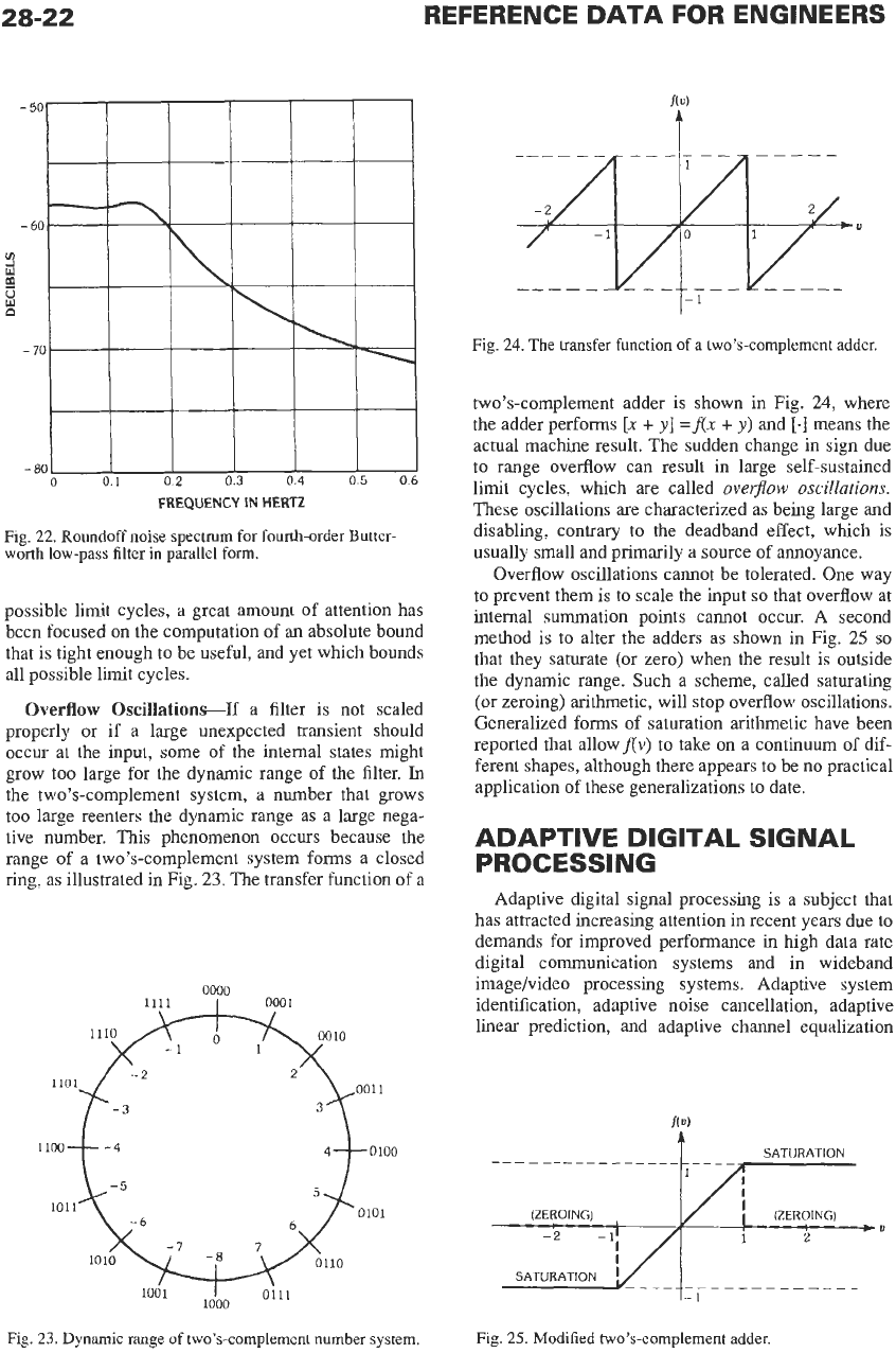
possible limit cycles, a great amount of attention has
been focused
on
the computation of an absolute bound
that is tight enough to be useful, and yet which bounds
all possible limit cycles.
Overflow
Oscillation+If
a filter is not scaled
properly or if a large unexpected transient should
occur at
the
input, some of the internal states might
grow too large for the dynamic range of the filter.
In
the two’s-complement system, a number that grows
too
large reenters the dynamic range as a large nega-
tive number. This phenomenon occurs because the
range of a two’s-complement system forms a closed
ring, as illustrated in Fig.
23.
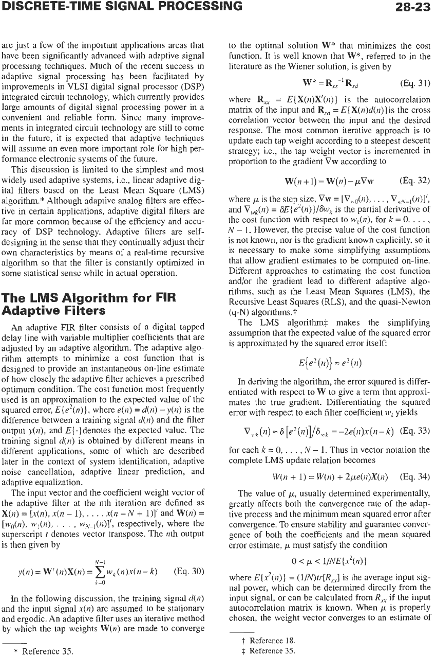
The transfer function of a
0000
1111
1
0001
I
Fig.
24. The
transfer function of a two’s-complement adder.
two’s-complement adder is shown in Fig.
24,
where
the adder performs
[x
+
y]
=f(x
+
y)
and
[.]
means the
actual machine result. The sudden change in sign due
to range overflow can result
in
large self-sustained
limit cycles, which are called
overflow
oscillations.
These oscillations are characterized as being large and
disabling, contrary to the deadband effect, which is
usually small and primarily a source of annoyance.
Overflow oscillations cannot be tolerated. One way
to prevent them is to scale the input
so
that overflow at
internal summation points cannot occur. A second
method is to alter the adders as shown in Fig.
25
so
that they saturate (or zero) when the result is outside
the dynamic range. Such a scheme, called saturating
(or zeroing) arithmetic, will stop overflow oscillations.
Generalized forms of saturation arithmetic have been
reported that allow
f(v)
to take
on
a continuum of dif-
ferent shapes, although there appears to be
no
practical
application of these generalizations
to
date.
ADAPTIVE DIGITAL SIGNAL
PROCESSING
Adaptive digital signal processing is a subject that
has attracted increasing attention in recent years due to
demands for improved performance
in
high data rate
digital communication systems and in wideband
imagehide0 processing systems. Adaptive system
identification, adaptive noise cancellation, adaptive
linear prediction, and adaptive channel equalization
f(u)
A
SATURATION
-1
Fig.
23.
Dynamic range of two’s-complement number system. Fig.
25.
Modified two’s-complement adder.
DISCRETE-TIME SIGNAL PROCESSING
28-23
are
just
a
few of the important applications areas that
have been significantly advanced with adaptive signal
processing techniques. Much of the recent success in
adaptive signal processing has been facilitated by
improvements
in
VLSI
digital signal processor (DSP)
integrated circuit technology, which currently provides
large amounts
of
digital signal processing power in a
convenient and reliable form. Since many improve-
ments in integrated circuit technology are still to come
in the future, it is expected that adaptive techniques
will assume
an
even more important role for high per-
formance electronic systems
of
the future.
This discussion is limited
to
the simplest and most
widely used adaptive systems, i.e., linear adaptive dig-
ital filters based on the Least Mean Square (LMS)
algorithm." Although adaptive analog filters are effec-
tive
in
certain applications, adaptive digital filters are
far more common because of the efficiency and accu-
racy of DSP technology. Adaptive filters
are
self-
designing
in
the sense that they continually adjust their
own characteristics by means of
a
real-time recursive
algorithm
so
that the filter is constantly optimized in
some statistical sense while in actual operation.
The LMS Algorithm for
FIR
Adaptive
Fi
I
t
e
rs
An
adaptive
FIR
filter consists of
a
digital tapped
delay line with variable multiplier coefficients that
are
adjusted by an adaptive algorithm. The adaptive algo-
rithm attempts to minimize
a
cost function that is
designed to provide
an
instantaneous on-line estimate
of how closely the adaptive filter achieves a prescribed
optimum condition. The cost function most frequently
used is
an
approximation to the expected value of the
squared error,
E{
e'@)],
where
e(n)
=
d(n)
-
y(n)
is the
difference between
a
training signal
d(n)
and the filter
output
y(n),
and
E{
.]denotes the expected value. The
training signal
d(n)
is obtained by different means in
different applications, some of which are described
later in the context of system identification, adaptive
noise cancellation, adaptive linear prediction, and
adaptive equalization.
The input vector and the coefficient weight vector of
the adaptive filter at the nth iteration
are
defined as
X(n)
=
[x(n),
x(n
-
l),
.
.
.
,
x(n
-
N
+
l)]'
and
W(n)
=
[wo(n),
wl(n),
. .
.
,
~~~-~(n)]',
respectively, where the
superscript
t
denotes vector transpose. The nth output
is then given by
N-1
y(n)
=
W'(n)X(n)
=
zw,(n)x(n-k)
(Eq.
30)
k=O
In
the following discussion, the training signal
d(n)
and the input signal
x(n)
are assumed to be stationary
and ergodic. An adaptive filter uses
an
iterative method
by which the tap weights
W(n)
are made to converge
to the optimal solution
W*
that minimizes the cost
function. It is well known that
W*,
referred to in the
literature
as
the Wiener solution, is given by
W
*
=
RXy-'
Rxd
(Eq.
31)
where
R,
=
E{X(n)X'(n)]
is the autocorrelation
matrix of the input and
Rxd
=
E(X(n)d(n)]is the cross
correlation vector between the input and the desired
response. The most common iterative approach is to
update each tap weight according to a steepest descent
strategy; i.e., the tap weight vector
is
incremented in
proportion to the gradient
Vw
according to
W(n+l)= W(n)-pVw
(Eq.
32)
where pis the step size,
Vw
=
[V,,(n),
.
.
.
,
V+vw-l(n)]',
and
V,,(n)
=
6E{
e2(n)]/Swk
is the partial derivative of
the cost function with respect to
wk(n),
for
k
=
0,
. . .
,
N
-
1.
However, the precise value of the cost function
is not known, nor is the gradient known explicitly,
so
it
is necessary to make some simplifying assumptions
that allow gradient estimates to be computed on-line.
Different approaches to estimating the cost function
and/or the gradient lead to different adaptive algo-
rithms, such as the Least Mean Squares (LMS), the
Recursive Least Squares (RLS), and the quasi-Newton
(q-N) algorithms.'f
The LMS algorithm3 makes the simplifying
assumption that the expected value of the squared error
is approximated by the squared error itself:
In
deriving the algorithm, the error squared is differ-
entiated with respect to
W
to give
a
term that approxi-
mates the true gradient. Differentiating the squared
error with respect to each filter coefficient
wi
yields
V,,(i~)=6[e~(n)]/8,~
=-2e(n)x(n-k)
(Eq.
33)
for each
k
=
0,
.
.
.
,
N
-
1.
Thus
in vector notation the
complete LMS update relation becomes
W(n
+
1)
=
W(n)
+
2pe(n)X(n)
(Eq.
34)
The value of
p,
usually determined experimentally,
greatly affects both the convergence rate of the adap-
tive process and the minimum mean squared error after
convergence. To ensure stability and guarantee conver-
gence of both the coefficients and the mean squared
error estimate,
p
must satisfy the condition
0
<
p
<
l/NE(2(n)]
where
E[x2(n)]
=
(l/N)tr[R,]
is the average input sig-
nal power, which can be determined directly from the
input signal, or can be calculated from
R,
if the input
autocorrelation matrix is known. When
p
is properly
chosen, the weight vector converges to an estimate of
t
Reference
18.
$
Reference
35.
*
Reference
35.
28-24
REFERENCE
DATA
FOR ENGINEERS
the Wiener solution. In practice, because of gradient
noise, the weight vector converges
to
a solution that
constantly fluctuates about
W*.
It has been shown that
the estimate of
W*
achieved by the LMS algorithm is
an unbiased estimate
of
the true Wiener solution.
The
LMS
Algorithm for
IIR
Adaptive
Fi
I
te rs
The MSE approximation that led to the conventional
LMS algorithm for
FIR
filters has also been applied to
the general class
of
IIR filter.* Recall that a direct form
IIR digital filter is characterized by a difference equa-
tion,
N,
y(n)
=
x
bkx(n
-
k)+
xaky(n
-
k)
(Eq.
35)
where the
b,s
are the coefficients that define the zeros
of the filter and the
aks
define the poles. The LMS
adaptive algorithm for IIR filters is derived in a similar
manner as in the FIR case, although the recursive rela-
tion of Eq.
35
is used instead
of
the convolutional sum
to characterize the input-output relationship
of
the
fil-
ter. The IIR derivation is more complicated because
the recursive terms
on
the right side of Eq.
35
depend
on
past values
of
the filter coefficients.
If
the derivatives of the squared error function are
calculated using the chain rule,
so
that all first order
dependencies are taken into account, the result is
k=O
k=l
L
J
where
k
=
0,.
.
.,
N,
(Eq. 36b)
This procedure does not generate a closed form
expression for the gradient as it did in the
FIR
case, but
it
does result
in
a mechanism by which the gradient
can be generated recursively using Eq. 36. Note that
Eq. 36a consists of
Nh
“all-pole” filters, where the
input to the k-th filter is simply the input signal shifted
by k time steps; similarly, Eq. 36b represents a similar
bank of filters, but where the input to the k-th filter is
the shifted output signal
y(n
-
k). Strictly speaking,
Eqs. 36a and b require
N,
+
Nb
distinct filters, one for
each of the gradient terms. However, in practice it is
usually assumed that the filter coefficients are slowly
varying
in
comparison to the signal frequency content,
so
that within a shift of
N,
or
Nb
time samples, the fil-
ters can be treated as though they are time-invariant.
With this assumption all of the gradient components
represented by Eq. 36a can be generated by a single
all-pole gradient filter whose input is x(n).
Similarly, the gradient terms in
Eq.
36b can be pro-
duced with a second filter that is identical to the first,
but which uses
y(n)
as the input signal. Then time-
shifted outputs from these filters will serve as accurate
approximations to the true gradient components repre-
sented by Eqs. 36a and b. This assumption of “station-
arity” in the input and output gradient filters is justified
by imposing slow parameter variation by choosing a
small step size.
In
the adaptive filtering literature, the
filter represented by Eq. 36a is typically called the
input gradient filter, whereas the one represented by
Eq. 36b is the output gradient filter. Similar concepts
are found in the fields of automatic control and analog
circuit theory, where such filters are typically called
input and output sensitivity filters
It is known that the use
of
the output error in the for-
mulation
of
the cost function prevents bias in the solu-
tion due to noise in the desired signal. However, the
effect of
this
recursion is to make the problem nonlin-
ear in terms of the coefficient parameters. The current
filter parameters now depend upon previous filter coef-
ficients, which are time-varying. This can lead
to
MSE
surfaces that are not quadratic in nature. There are
many examples in the literature for which the MSE
surface demonstrates one or more local minima,
in
addition to the global minimum.
In
these cases the
LMS algorithm, being a gradient search technique,
may converge to a local minimum, resulting in poor
performance when used in practical applications.
Therefore, in general, practicing engineers are often
reluctant to use the
LMS
IIR
adaptive filter in practical
applications due to its uncertain performance.
Generic Applications
of
Adaptive Methods
There
are
four basic configurations in which adap-
tive filters are typically used to solve practical engi-
neering problems:?
System Identification Configuration-An
adap-
tive filter
is
said to be used in the system identification
configuration when both the adaptive filter and an
unknown
system are excited by the same input signal
x(n),
the system outputs are compared to form the
*
Reference
35.
t
Reference
13.
DISCRETE-TIME
SIGNAL
PROCESSING
Adaptive
b
Filter
28-25
v(n)
error signal
e(n)
=
d(n)
-
y(n),
and the parameters of
the adaptive filter are iteratively adjusted to minimize
some specified function
of
the error
e(n).
In
the system
identification configuration, shown in Fig. 26, the
desired signal is produced as the output
of
an unknown
plant whose input is accessible for excitation. When
the minimum of the cost function is achieved and the
adaptive filter parameters have converged to stable val-
ues, the adaptive filter provides a model of the
unknown system, in the sense that the adaptive process
has formed the best approximation
it
can in the MSE
sense using the structure imposed by the adaptive sys-
tem. The converged coefficients provide good esti-
mates of the model parameters.
In
order for the adaptive system to form a good
model
of
the unknown system at all frequencies, it is
important that the input signal have sufficiently rich
spectral content. For example, if the adaptive filter is
an FIR filter structure with
N
adjustable coefficients,
the input signal must contain at least
N
distinct fre-
quency components in order to uniquely determine the
set of coefficients that minimizes the MSE. A white
noise input signal is ideal because it excites all fre-
quencies with equal power. A broadband colored noise
input will also provide a good excitation signal, in the
sense of driving the adaptive filter to the minimum
MSE solution. Although, in general, the convergence
rate
of
the learning process will be slower than for
white noise inputs because the frequencies that are
excited with small power levels will converge slowly.
Many adaptive algorithms attempt
to
normalize (or
whiten) the input power spectrum in order to improve
the convergence rate
of
the learning process.*
The system identification configuration is a funda-
mental adaptive filtering concept that underlies many
applications of adaptive filters. The major attraction
of
the system identification configuration is that the train-
ing signal is automatically generated as the output of
x(n)
*
Reference 13.
e(n)
L
Unknown
d(n)
b
the unknown system. The disadvantage is that the
input of the unknown system must be accessible to be
excited by an externally applied input noise signal.
In
some applications obtaining a model of the unknown
system is the desired result, and the accuracy of the
adaptive coefficients is a primary concern.
In
other
applications it is not necessary that the unknown sys-
tem be identified explicitly, but rather that the adaptive
filter is required to model the
unknown
system only to
generate accurate estimates of its output signal. This
leads to the next configuration called adaptive noise
cancellation, which is really a variation
on
the funda-
mental theme of system identification.
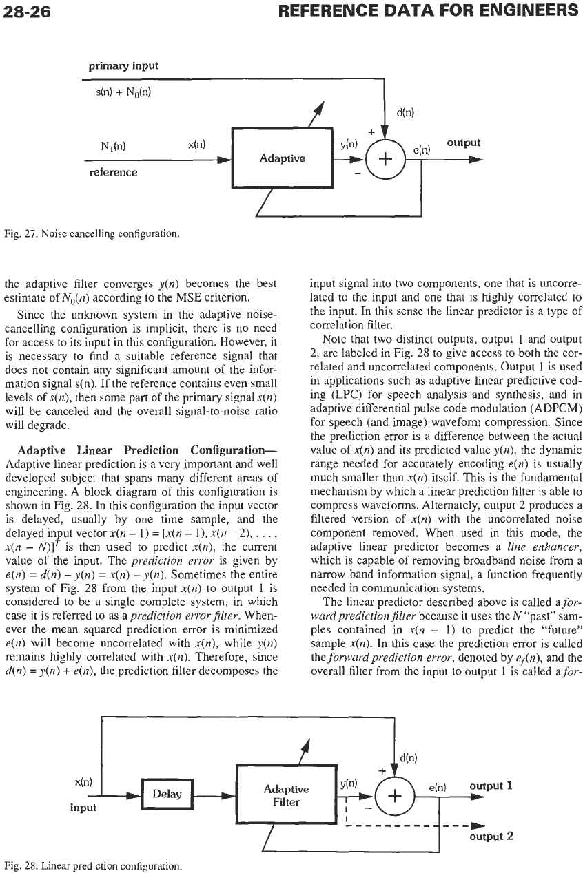
Adaptive Noise Cancelling Configuration-A
block diagram for an adaptive noise canceller is shown
in Fig. 27, where it is seen that the unknown system in
this configuration is not shown explicitly, nor is it
desired to identify the implicit unknown system in a
direct way. The primary signal is assumed to be the
sum
of
an information bearing signal
s(n)
and an addi-
tive noise component
N&),
which is uncorrelated
with
s(n).
The primary signal is used to train the adap-
tive noise canceller,
so
that
d(n)
=
s(n)
+
No(n)
and the
error signal becomes
e(n)
=
d(n)
-y(n)
=
s(n)
+No(n)
-
y(n).
The reference signal, which
is
used as the input to
the adaptive filter, should be a reference noise
Nl(n)
that is uncorrelated to
s(n),
but which is correlated in
an unknown way with
NO@).
The adaptive filter forms
an estimate of
N,,(n)
and subtracts this estimate from
the primary input signal, thereby forming in a good
estimate of the information signal at the output of the
noise canceller. Note that
System
input
so
that minimizing
E[
I
e(n)
I
*]
will also minimize
E[
IN&)
-
y(n)
1'1
because the first term in Eq. 37 is
dependent only
on
the information signal
s(n)
and its
mean squared value cannot be affected by the adaptive
filter as long as
s(n)
and
Nl(n)
are
uncorrelated. After
output
Fig.
26.
System
identification configuration.
28-26
Fig.
27.
Noise cancelling configuration.
the adaptive filter converges
y(n)
becomes
the
best
estimate of
N&)
according to the
MSE
criterion.
Since the unknown system in the adaptive noise-
cancelling configuration is implicit, there is
no
need
for access to its input in this configuration. However, it
is necessary to find a suitable reference signal that
does not contain any significant amount of the infor-
mation signal
s(n).
If the reference contains even small
levels
of
s(n),
then some part of the primary signal
s(n)
will be canceled and the overall signal-to-noise ratio
will degrade.
Adaptive Linear Prediction Configuration-
Adaptive linear prediction is a very important and well
developed subject that spans many different areas of
engineering. A block diagram of this configuration is
shown
in
Fig. 28.
In
this configuration the input vector
is delayed, usually by one time sample, and the
delayed input vector
n(n
-
1)
=
[x(n
-
l),
x(n
-
2),
.
.
.
,
x(n
-
NIT
is then
used
to predict
x(n),
the current
value of the input. The prediction error is given by
e(n)
=
d(n)
-
y(n)
=
x(n)
-
y(n).
Sometimes the entire
system of Fig. 28 from the input
x(n)
to output 1 is
considered to be a single complete system, in which
case it is referred to as aprediction errorfilter. When-
ever the mean squared prediction error is minimized
e(n) will become uncorrelated with
x(n),
while
y(n)
remains highly correlated with
x(n).
Therefore, since
d(n)
=
y(n)
+
e@), the prediction filter decomposes the
input signal into two components, one that is uncorre-
lated to the input and one that is highly correlated to
the input.
In
this sense the linear predictor is a type of
correlation filter.
Note that two distinct outputs, output
1
and output
2, are labeled in Fig. 28 to give access to both the cor-
related and uncorrelated components.
Output
1
is used
in applications such as adaptive linear predictive cod-
ing (LPC) for speech analysis and synthesis, and in
adaptive differential pulse code modulation (ADPCM)
for speech (and image) waveform compression. Since
the prediction error is a difference between the actual
value of
x(n)
and its predicted value
y(n),
the dynamic
range needed for accurately encoding e(n) is usually
much smaller than
x(n)
itself. This is
the
fundamental
mechanism by which
a
linear prediction filter is able to
compress waveforms. Alternately, output
2
produces a
filtered version of
x(n)
with the uncorrelated noise
component removed. When used in this mode, the
adaptive linear predictor becomes a line enhancer,
which is capable of removing broadband noise from a
narrow band information signal, a function frequently
needed in communication systems.
The linear predictor described above is called a for-
wardprediction filter because it uses the
N
“past”
sam-
ples contained in
x(n
-
1)
to
predict the “future”
sample
x(n).
In
this case the prediction error is called
the forward prediction error, denoted by
ef(n),
and the
overall filter from the input to output
1
is
called afor-
x(n)
input
w
output
2
Fig.
28.
Linear prediction configuration.
DISCRETE-TIME SIGNAL PROCESSING
28-27
ward prediction error filter.
The linear prediction
problem can also be formulated as backward linear
prediction, in which case the filter is used to estimate
the sample
x(n
-
N)
from the
N
“future” samples con-
tained in
x(n)
=
[x(n),
x(n
-
l),
.
.
.
,
x(n
-
N
+
l)]‘.
In
this case, the prediction filter is called the
backward
prediction filter,
the prediction error is called the
back-
ward prediction error,
denoted
e&),
and the overall
filter is called the
backward prediction error filter.
A
combination of forward and backward prediction is
used in the conventional adaptive lattice filters, where
the
uncorrelated properties of the prediction error
leads to excellent learning characteristics.*
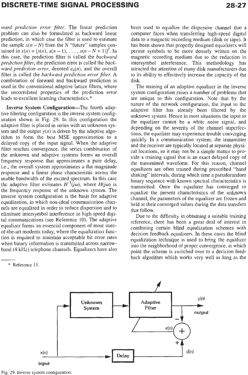
Inverse
System Configuration-The fourth adap-
tive filtering configuration is the inverse system config-
uration shown in Fig.
29.
In
this configuration the
adaptive filter is placed in series with an unknown sys-
tem and the output
y(n)
is driven by the adaptive algo-
rithm to form the best
MSE
approximation to a
delayed copy of the input signal. When the adaptive
filter reaches convergence, the series combination of
the
unknown
and adaptive systems forms an overall
frequency response that approximates a pure delay,
i.e., the overall system approximates a flat magnitude
response and a linear phase characteristic across the
usable bandwidth of the excited spectrum.
In
this
case
the adaptive filter estimates
H-’@o),
where
HGw)
is
the frequency response of the unknown system. The
inverse system configuration is the basis for adaptive
equalization, in which non-ideal communication chan-
nels are equalized
in
order to reduce dispersion and to
eliminate intersymbol interference
in
high-speed digi-
tal communications (see Reference
10).
The adaptive
equalizer forms an essential component of most state-
of-the-art modems today, where the equalization func-
tion is required to maintain acceptable bit error rates
when binary information is transmitted across narrow-
band
(4
kHz) telephone channels. Equalizers have also
been used to equalize the dispersive channel that a
computer faces when transferring high-speed digital
data to a magnetic recording medium (disk or tape). It
has been shown that properly designed equalizers will
permit symbols to be more densely written
on
the
magnetic recording medium due to the reduction
in
intersymbol interference. This methodology has
attracted the attention of many disk manufacturers due
to its ability to effectively increase the capacity of
the
disk.
The training of an adaptive equalizer in the inverse
system configuration raises a number of problems that
are unique to this configuration. Note that by the
nature
of
the network configuration, the input to the
adaptive filter has already been filtered by the
unknown system. Hence in most situations the input to
the equalizer cannot be a white noise signal, and
depending on the severity
of
the channel imperfec-
tions, the equalizer may experience trouble converging
quickly.
In
a communication system, the transmitter
and the receiver are typically located at separate physi-
cal locations,
so
it may not be a simple matter to pro-
vide a training signal that is an exact delayed copy of
the transmitted waveform. For this reason, channel
equalizers are often trained during prescribed “hand
shaking” intervals, during which time a pseudorandom
binary sequence with known spectral characteristics is
transmitted. Once the equalizer has converged
to
equalize the present characteristics of the unknown
channel, the parameters of the equalizer
are
frozen and
held at their converged values during the data transfers
that follow.
Due
to
the difficulty in obtaining a suitable training
reference, there has been a great deal of interest in
combining certain blind equalization schemes with
decision feedback equalizers.
In
these cases the blind
equalization technique is used to bring the equalizer
into the neighborhood of proper convergence, at which
point the scheme is switched over to a decision feed-
back algorithm which works very well as long as the
*
Reference
13.
i
Fig.
29.
Inverse system Configuration.
28-28
REFERENCE
DATA
FOR
ENGINEERS
equalizer remains in the neighborhood
of
its optimum
solution.
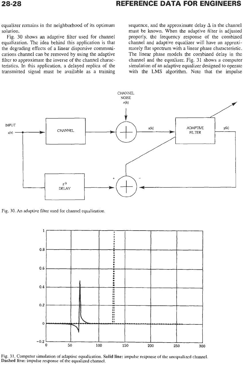
Fig.
30
shows an adaptive filter used for channel
equalization. The idea behind this application is that
the
degrading effects of a linear dispersive communi-
cations channel can be removed by using the adaptive
filter to approximate the inverse
of
the channel charac-
teristics.
In
this application, a delayed replica of the
transmitted signal must be available as a training
sequence, and
the
approximate delay
A
in the channel
must be known. When the adaptive filter is adjusted
properly, the frequency response of the combined
channel and adaptive equalizer will have
an
approxi-
mately flat spectrum with
a
linear phase characteristic.
The linear phase models the combined delay in the
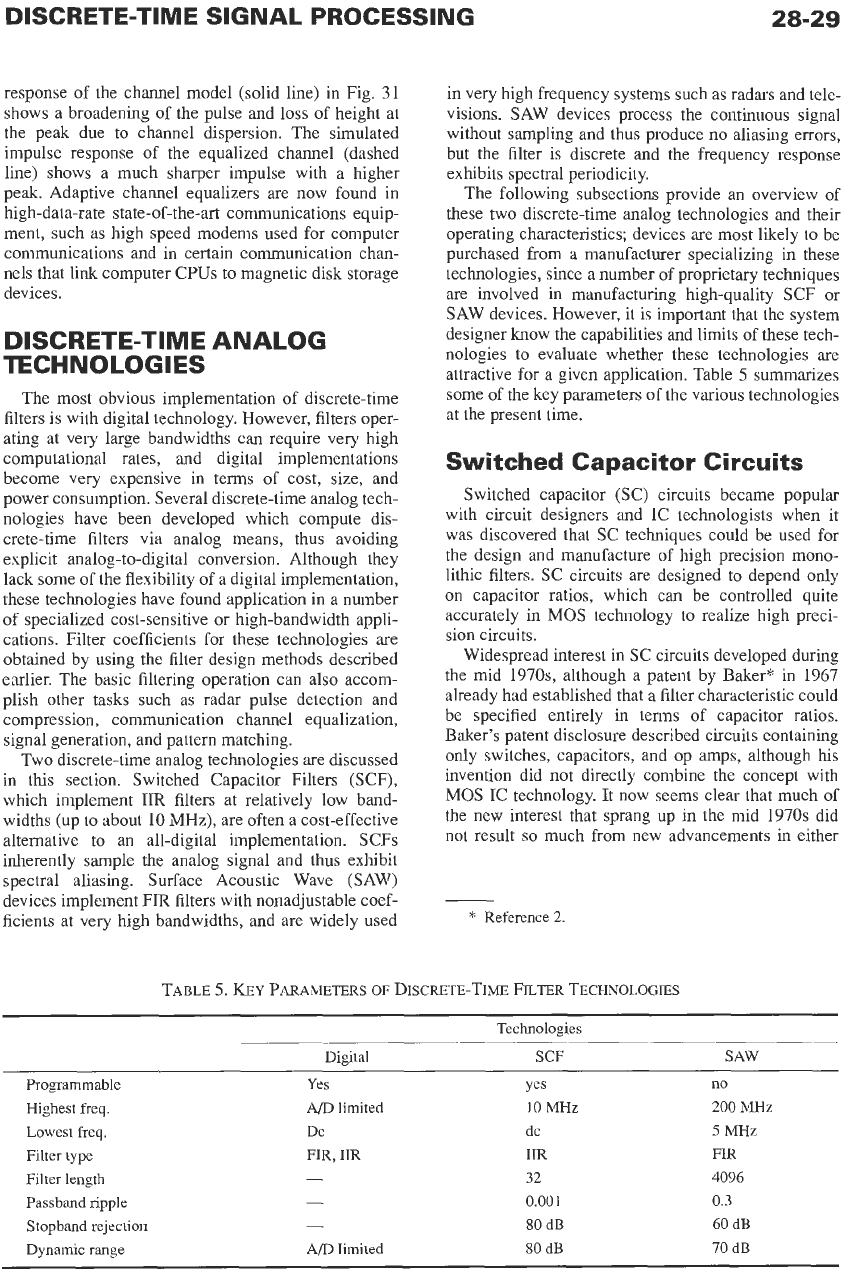
channel and the equalizer. Fig.
31
shows a computer
simulation
of
an adaptive equalizer designed to operate
with the
LMS
algorithm. Note that the impulse
CHANNEL
NOISE
n(k)
Fig.
30.
An adaptive filter used for channel equalization.
1
0.8
0.6
0.4
0.2
oi
q
1
1
1
-0.2
0
50
100
150
200
250
300
Fig.
31.
Computer simulation
of
adaptive equalization.
Solid line:
impulse response
of
the unequalized channel.
Dashed line:
impulse response
of
the equalized channel.
DISCRETE-TIME SIGNAL PROCESSING
28-29
response of the channel model (solid line) in Fig. 31
shows a broadening of
the
pulse and loss of height at
the peak due to channel dispersion. The simulated
impulse response of the equalized channel (dashed
line) shows
a
much sharper impulse with a higher
peak. Adaptive channel equalizers are now found in
high-data-rate state-of-the-art communications equip-
ment, such as high speed modems used for computer
communications and in certain communication chan-
nels that link computer CPUs to magnetic disk storage
devices.
TECHNOLOGIES
The most obvious implementation of discrete-time
filters is with digital technology. However, filters oper-
ating at very large bandwidths can require very high
computational rates, and digital implementations
become very expensive in terms of cost, size, and
power consumption. Several discrete-time analog tech-
nologies have been developed which compute dis-
crete-time filters via analog means, thus avoiding
explicit analog-to-digital conversion. Although they
lack some of the flexibility of a digital implementation,
these technologies have found application in a number
of specialized cost-sensitive or high-bandwidth appli-
cations. Filter coefficients for these technologies are
obtained by using the filter design methods described
earlier. The basic filtering operation can also accom-
plish other tasks such
as
radar pulse detection and
compression, communication channel equalization,
signal generation, and pattern matching.
Two discrete-time analog technologies
are
discussed
in
this section. Switched Capacitor Filters (SCF),
which implement IIR filters at relatively low band-
widths (up
to
about
10
MHz), are often a cost-effective
alternative to
an
all-digital implementation. SCFs
inherently sample the analog signal and thus exhibit
spectral aliasing. Surface Acoustic Wave (SAW)
devices implement
FIR
filters with nonadjustable coef-
ficients at very high bandwidths, and are widely used
in very high frequency systems such
as
radars and tele-
visions. SAW devices process the continuous signal
without sampling and thus produce
no
aliasing errors,
but the filter is discrete and the frequency response
exhibits spectral periodicity.
The following subsections provide an overview of
these two discrete-time analog technologies and their
operating characteristics; devices are most likely
to
be
purchased from a manufacturer specializing in these
technologies, since
a
number of proprietary techniques
are involved in manufacturing high-quality SCF or
SAW devices. However, it is important that the system
designer know the capabilities and limits
of
these tech-
nologies to evaluate whether these technologies are
attractive for a given application. Table
5
summarizes
some of the key parameters of the various technologies
at the present time.
Switched Capacitor Circuits
Switched capacitor (SC) circuits became popular
with circuit designers and IC technologists when it
was
discovered that SC techniques could be used for
the design and manufacture of high precision
mono-
lithic filters. SC circuits are designed to depend only
on
capacitor ratios, which can be controlled quite
accurately in
MOS
technology to realize high preci-
sion circuits.
Widespread interest in SC circuits developed during
the mid
1970s,
although a patent by Baker” in
1967
already had established that a filter characteristic could
be specified entirely in terms of capacitor ratios.
Baker’s patent disclosure described circuits containing
only switches, capacitors, and op amps, although his
invention did
not
directly combine the concept with
MOS
IC technology. It now seems clear that much of
the new interest that sprang up in the mid
1970s
did
not
result
so
much from new advancements in either
*
Reference
2.
TABLE
5.
KEY
PARAMETERS
OF
DISCRETE-TIME
FILTER
TECHNOLOGIES
Technologies
Digital
SCF
SAW
Programmable
Yes
Yes no
Highest
freq.
AD
limited
10
MHz
200
MHz
Lowest
freq.
Dc
dc
5
MHz
Filter length
-
32
4096
Passband ripple
-
0.001
0.3
Stopband rejection
-
80
dB 60
dB
Dynamic range
AD
limited
80
dB
70
dB
Filter type
FIR,
IIR
IIR
FIR
28-30
REFERENCE
DATA
FOR ENGINEERS
circuit theory or
IC
technology alone,
but
rather from
coupling these two areas in
an
effective way.
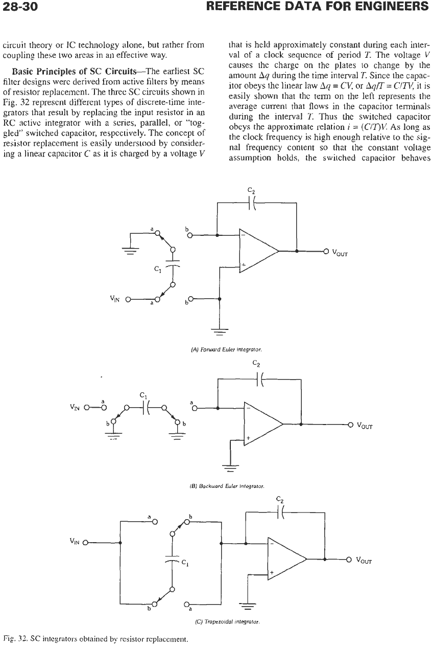
Basic Principles
of
SC Circuits-The earliest
SC
filter designs were derived from active filters by means
of resistor replacement. The three
SC
circuits shown in
Fig.
32
represent different types
of
discrete-time inte-
grators that result
by
replacing the input resistor
in
an
RC
active integrator with a series, parallel, or "tog-
gled" switched capacitor, respectively. The concept
of
resistor replacement
is
easily understood by consider-
ing a linear capacitor
C
as it
is
charged by a voltage
V
that is held approximately constant during each inter-
val of a clock sequence of period
T.
The voltage
V
causes the charge
on
the plates
to
change by the
amount
Aq
during the time interval
T.
Since
the
capac-
itor obeys the linear law
Aq
=
Cy
or
Aq/T
=
C/rV;
it is
easily shown that the term
on
the left represents the
average current that flows in the capacitor terminals
during the interval
T.
Thus the switched capacitor
obeys the approximate relation
i
=
(C/T)r/:
As long as
the clock frequency is high enough relative
to
the sig-
nal frequency content
so
that the constant voltage
assumption holds, the switched capacitor behaves
-
(A)
Forward Euler Integrator.
c2
-
(E)
Backward Euler Integrator.
(C)
Trapezoidal
integrator.
Fig.
32. SC
integrators obtained by resistor replacement.
DISCRETE-TIME SIGNAL PROCESSING
approximately like a resistor of value
Re,
=
(TIC).
When the frequency of the clock approaches the
Nyquist limit relative to the signal bandwidth, this
approximation begins to break down, and it is neces-
sary
to consider the details of the switch phasing in
order to determine an accurate model for the perfor-
mance of the SC circuit.
As
it
became better understood that resistor replace-
ment techniques are inaccurate for switching rates near
the Nyquist limit, SC circuit designers began to char-
acterize charge transfer relationships in SC circuits
with discrete-time difference equations and to apply
the theory of discrete time systems to analyze perfor-
mance. It was learned that
if
the output voltage is sam-
pled on the “a” switch phase, then the network shown
in Fig. 32a behaves as a forward Euler integrator, the
network of Fig. 32b as a backward Euler integrator,
and that of Fig. 32c as a trapezoidal integrator. Subse-
quently, Broderson et.
al.*
showed how high quality
SC filters can be derived from the “leapfrog” active fil-
ter structure, a particular form of a doubly terminated
LC ladder, by using SC integrator replacements.
If a toggled switched capacitor, like the one used to
replace the input resistor in the trapezoidal integrator
of Fig. 32c, is used
to
replace every resistor in an arbi-
trary RC active filter, the analog structure is trans-
formed into an SC structure according to the bilinear-z
transformation discussed earlier. If each phase of the
biphase clock has period
T,
the effective sampling rate
becomes
2/T
because the toggle switched capacitor has
identical behavior on each phase.
In
MOS
transistors, there normally is a rather large
nonlinear parasitic capacitance
C,
between the bottom
plate and the substrate, as well as a considerably
smaller parasitic capacitance
Cp
between the top plate
and the substrate.
C,
can be as much as
20%
of the fab-
ricated capacitor, and is rather difficult to predict or
compensate.
Cp
is normally an order of magnitude
smaller, although its presence can disturb a sensitive
design significantly. It is important for SC circuits to
be designed with the bottom plate of all capacitors
grounded or switched between a voltage source and
ground
so
that excess charge accumulated by the para-
sitic during the charging phase is harmlessly dis-
charged to ground and does not affect the
characteristics of the circuit. It is clear that a toggled
switched capacitor cannot be made parasitic insensi-
tive in general, since the top and bottom plates must
perfom
the same function on alternate phases. Despite
efforts to compensate for parasitics in the “bilinear
switched capacitor,” it was largely rejected by IC tech-
nologists as impractical because it led to too much
uncontrolled variation in the characteristics of the final
SC circuits.
Note that the forward and backward Euler integra-
tors of Fig.
32
are insensitive with respect to both the
top plate and bottom plate parasitics. For this reason
*
Reference
5.
these types of integrators became more successful than
the bilinear integrator, and were subsequently used in
many design methods that were eventually published.
Broderson et
al.?
described a set of practical consider-
ations for
MOS
implementation of SC circuits that
became standard rules of thumb for SC circuit design-
ers:
(1)
switched capacitor “resistors” should not close
an on amp feedback path;
(2)
there should be no float-
ing nodes; (3) at least one plate of every capacitor
should be connected to a voltage source or switched
between voltage sources; and
(4)
the noninverting op
amp input should be kept at a constant voltage (usually
grounded) or switched between voltage sources.
Although these should be guidelines rather than strict
rules, they have withstood the test of time in the sense
that most IC technologists tend to reject designs that
violate these conditions. The later book by Ghausi and
Lakerf incorporated these rules into the design proce-
dure, representing a change of philosophy from the
resistor and integrator replacement techniques that
dominated earlier designs.
Switched Capacitor
Filters
for
Voice Quality
CODECs-One successful application of switched
capacitor circuit technology has been in the realization
of analog pre- and post-filters required for digital voice
transmission in modem telephone channels. The A/D
and D/A conversion, as well as some additional signal
conditioning (companding, etc.), is implemented with
an
IC
referred to as a CODEC (coder-decoder). A
sin-
gle IC contains the “transmit” filter to handle transmis-
sion in the forward direction, the “receive” filters to
handle the returned voice signal, as well as other cir-
cuits required for signal conditioning. The industry
standard for the digital sampling rate is
8
kHz, which
is designed to prevent aliasing on a
4-kHz
telephone
channel. Prior to SC circuit technology, the transmit
and receive filtering was done with an active filter that
was implemented with expensive hybrid fabrication
techniques. With switched capacitor circuit tech-
niques, the goal of integrating the transmit and receive
filters together with the CODEC, while meeting the
rather strict system specifications, became reachable.
The philosophy is
to
switch the SC filters at a veq7
high rate (usually
256
kHz) relative to the 8-kHz sam-
pling rate of the CODEC
so
that sampled data effects
in the SC circuits are negligible, and for all intents and
purposes the SC pre- and post-filters function as ana-
log filters. The transmit filter must have a low-pass
characteristic within a
0+0.01
dB
tolerance in the pass-
band up to a ripple cutoff frequency
of
3.4
kHz.
In
the
receive channel, a post-filter is required following the
D/A converter to smooth the staircase waveform that
results from
the
reconstruction process. The receive
fil-
ter is a low-pass filter with a cutoff at 3.4
kHz,
which is
essentially the same as the antialiasing transmit filter.
i.
Reference
5.
Reference
11.