Middleton W.M. (ed.) Reference Data for Engineers: Radio, Electronics, Computer and Communications
Подождите немного. Документ загружается.

14-2
Turn-off Losses
Snubbers and Clamps
Switch-Mode Converter Control
Voltage-Mode Control
Current-Mode Control
Resonant Transistor Circuits
Power Factor Correction Circuits
Power Factor Definition
International Regulatory Standards
Active Power Factor Correction
Filter Circuits and Design
14-39
Inductor-Input Filter Design
Capacitor-Input Filter Design
Harmonic Currents and Power Factor
Phase-Controlled-Thyristor Filter Design
Resonant-Filter Design
DC-Output Power Supplies
14-43
Unregulated Power Supplies
Linear Regulated Power Supplies
Phase-Control Power Supplies
Switchmg Power Supplies
Distributed Power Supplies
AC-Output Power Supplies
14-46
AC Voltage Regulators
DC-AC Inverters
C ycloconverters
POWER ELECTRONICS
14-3
CHARACTERISTICS
OF
POWER
SEMICONDUCTOR DEVICES
This section briefly describes the terminal properties
of various types of power semiconductor devices to aid
in understanding their operation in power conversion
equipment. Power semiconductor devices discussed
are rectifiers, including fast recovery and Schottky;
bipolar, field-effect, and insulated-gate transistors; thy-
ristors, MOS-controlled thyristors, and triacs; and
voltage transient clippers.
Rectifiers
Voltage and Current Ratings-Silicon-rectifier
ratings* are generally expressed in terms of reverse-
voltage ratings and of mean-forward-current ratings in
a half-wave circuit operating from a 60-hertz sinusoi-
dal supply and into a purely resistive load.
There are three reverse-voltage ratings of impor-
tance:
Peak transient reverse voltage
VRM
Maximum repetitive reverse voltage
V,,(,,)
Working peak reverse voltage
vRM(w
kg)
Peak transient reverse voltage
(VRM)
is the rated maxi-
mum value of any nonrecurrent surge voltage, and this
value must not be exceeded under any circumstances,
even for a microsecond. Maximum repetitive reverse
voltage
(VRM(rep))
is the maximum value of reverse
voltage that may be applied recurrently, e.g., in every
cycle, and will include any circuit oscillatory voltage
that may appear
on
the sinusoidal supply voltage.
Working peak reverse voltage
(VRM(wkg))
is the crest
value of the sinusoidal voltage of the supply at its max-
imum limit. The manufacturer generally recommends
a
VRM(wkg)
that has an appreciable safety margin in rela-
tion to the
V,,
to allow for the commonly experienced
transient overvoltages on power mains.
Three forward-current ratings are similarly of
importance:
Nonrecurrent surge current
IFM(surge)
Repetitive peak forward current
IFM(1ep)
Average forward current
IF(Z!")
Silicon diodes have comparatively small thermal mass,
and care must be taken to ensure that short-term over-
load currents are limited. The nonrecurrent surge
CUT-
rent
is
sometimes given
as
a single value that must not
be exceeded at any time, but it
is
more generally given
in the form of a graph of permissible surge current ver-
sus
time. It is important to observe whether the surge-
*
For a complete list
of
silicon-rectifier ratings, re-
fer to the EIA-JEDEC
Recommendations
for
Letter
Symbols, Abbreviations, Terms and Definitions
for
Semiconductor Device Data Sheets and Spec$cations,
published by Electronic Industries Association, 2001
I
Street,
NW,
Washington,
DC
20006.
current scale is marked in peak, rms, or average value
for the data to be correctly interpreted. The repetitive
peak forward current is the peak value of the forward
current reached in every cycle and excludes random
peaks caused by transients. Its relation to the average
forward current depends
on
the circuit used and
on
the
load that is applied. For example, the repetitive peak is
about three times the average for a half-wave or bridge
circuit working into a resistive load; it may be many
times greater when the same circuits work into capaci-
tive loads.
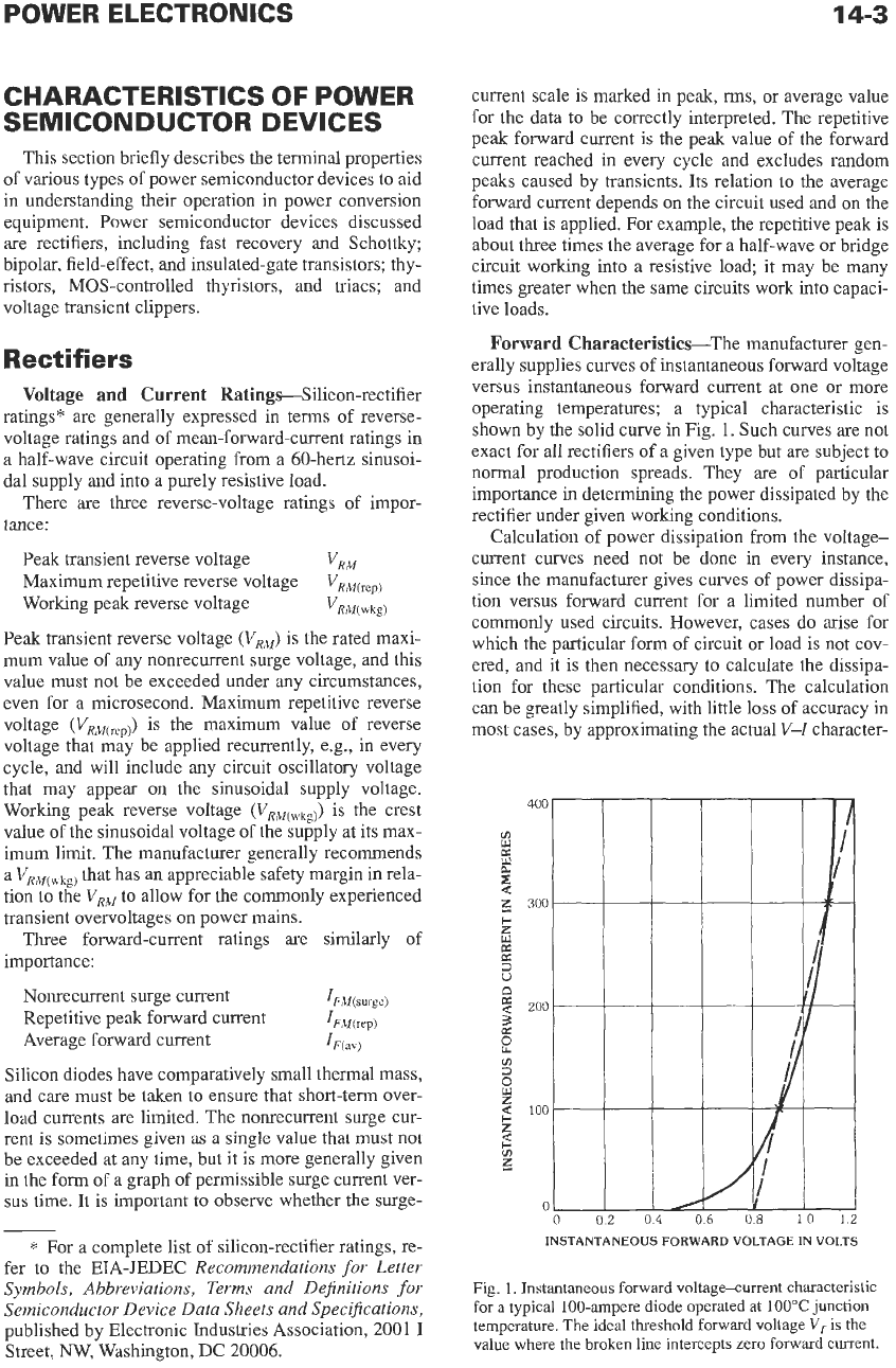
Forward Characteristics-The manufacturer gen-
erally supplies curves of instantaneous forward voltage
versus instantaneous forward current at one or more
operating temperatures; a typical characteristic is
shown by the solid curve in Fig.
1.
Such curves are not
exact for all rectifiers
of
a given type but are subject to
normal production spreads. They are of particular
importance in determining the power dissipated by the
rectifier under given working conditions.
Calculation of power dissipation from the voltage-
current curves need not be done in every instance,
since the manufacturer gives curves
of
power dissipa-
tion versus forward current for a limited number of
commonly used circuits. However, cases do arise for
which the particular form of circuit or load is not cov-
ered, and it is then necessary to calculate the dissipa-
tion for these particular conditions. The calculation
can be greatly simplified, with little loss
of
accuracy in
most cases, by approximating the actual
V-I
character-
INSTANTANEOUS FORWARD
VOLTAGE
IN
VOLTS
Fig.
1.
Instantaneous forward voltage-current characteristic
for
a typical
100-ampere
diode operated
at
100°C
junction
temperature.
The
ideal threshold forward voltage
V,
is
the
value where the broken line intercepts zero forward current.
istic curve
to
a
straight line, as shown by the broken
line in Fig.
1.
The approximate characteristic corre-
sponds to that of
a
fixed voltage (the threshold voltage)
plus
a
fixed resistance (the slope resistance). For any
shape of current waveform, the power dissipated at
constant voltage is the product
of
the
average current
and this fixed voltage, while the power dissipated
at
constant resistance is the product of the square of the
rms
current and
this
fixed resistance. Thus, the follow-
ing simple equation can be used:
where,
P
is the forward power dissipation,
is the average forward current through the rec-
tifier, averaged over one complete cycle,
is the
rms
value of the forward current
through the rectifier,
V,
is the threshold voltage, and
R,
is the slope resistance.
For the best accuracy, the straight-line approxima-
tion should be drawn through points on the current
curve corresponding to 50% and 150% of the peak
current at which the rectifier is to be used. Thus, in Fig.
1
the broken line would correspond
to
a
peak working
current of 200 amperes.
Carrier Storageon switching from forward con-
duction to reverse blocking, a silicon diode cannot
immediately revert
to
its blocking state because of the
presence of the stored carriers in the junction. These
have the effect of allowing current to flow in reverse,
as
through a forward-biased junction, when reverse
voltage is applied. The current is limited only by the
external voltage and circuit parameters. However, the
carriers are rapidly removed from the junction both by
internal recombination and by the sweep-out effect of
the reverse current, and when this has happened, the
diode reverts to its blocking condition in which only
a
low leakage current flows. This sudden cessation of
a
large reverse current can cause objectionable voltage
transients if there is appreciable circuit inductance and
surge-suppression components have not been included.
The reverse current due to carrier storage is not exces-
sive in normal operation of power rectifier circuits and
does not in itself constitute
a
hazard; however, its
effect can sometimes lead
to
complications in switch-
ing arrangements. For example, in an inductively
loaded circuit, the current will “free-wheel” through
the diodes after the supply has been removed until the
inductive energy has been discharged. Should the sup-
ply be reapplied while this process is going on, some
of
the diodes will be required to conduct in a forward
direction, but others will be required to block; while
the latter are recovering from the carrier storage
injected by the free-wheeling current, the short-circuit
across the supply can cause
a
damaging surge current
to
flow.
A
technique for reducing this problem is
to
use
“fast-recovery’’ rectifiers. These rectifiers are tailored
to
operate in high-frequency circuits with reduced and
specified amounts of recovered charge. The devices
change from conducting reverse current to leakage
current in
a
“nonabrupt” manner. The finite rate of
change in current reduces the transient voltages that
appear on the power semiconductors and other circuit
elements.
Schottky Rectifiers
The Schottky rectifier has the same terminal charac-
teristics as do conventional and fast-recovery rectifiers;
that is, it conducts current in one direction and blocks
voltage of one polarity. Rather than rely on a pn junc-
tion for rectification, the Schottky diode uses
a
metal-
to-semiconductor contact. Depending on the metal, the
forward voltage drop is typically one-half that of a
conventional silicon pn rectifier. The reverse voltage
rating is lower than that of
a
pn rectifier, being on the
order of 50 to 200 volts. The rectifying action
of
the
Schottky rectifier depends upon the majority carriers,
so
there is very little reverse current caused by minor-
ity-carrier recombination. Therefore, these devices are
characterized by very low recovered charge and
as
such are suitable for high-frequency rectification, up
to
typically
1
to
5
MHz. The devices are used extensively
as
rectifiers on the low-voltage windings of high fre-
quency switching mode power supplies. The
output
voltage of these systems is typically
5
volts dc, and
they operate typically at 20 kHz
to
1
MHz. The Schot-
tky rectifiers operate in these systems with consider-
ably lower conduction and switching losses than
silicon pn rectifiers.
Zener Diodes
“Zener” is the name given to
a
class of silicon
diodes having
a
sharp turnover characteristic at
a
par-
ticular reverse voltage,
as
shown
in
Fig. 2. If such
a
diode is operated
on
this part of its characteristic, no
breakdown (in the sense
of
dielectric breakdown)
occurs, and the process is reversible without damage.
The steepness of the reverse
part
of the current-volt-
age characteristic in the turnover region makes these
diodes excellent elements for voltage reference and
voltage regulation.
The temperature coefficient for
a
typical range of
zener diodes is shown
in
Fig.
3.
It
will be seen that the
coefficient changes from negative to positive
in
the
region
of
5
volts. Use is sometimes made of
this
phe-
nomenon to match diodes of opposite coefficient to
produce
a
series pair having
a
low effective tempera-
ture coefficient in combination.
Zener diodes are used to provide stable reference
voltages for electronic control circuits and
as
a voltage
reference for closed-loop regulating systems in which
the actual voltage is compared
to
the reference voltage
in order to develop an error signal. They are available
POWER ELECTRONICS
14-5
REVERSE VOLTAGE
IN
VOLTS
Fig.
2.
Typical reverse characteristics for
three
low-
voltage zener diodes
of
1-watt rating. (From
J.
M.
Waddell
and
D.
R.
Coleman, “Zener Diodes-Their Properties and
Applications,”
Wireless World,
Vol. 66,
No.
1,
p. 18, Fig.
2;
January 1960.
0
1959, Iliffe Electrical Publications, Ltd.,
London, England.)
+o
1
+O
05
0
-0
05
-0
1
2
4
6
S
10
12
14
16
18
Fig.
3.
Temperature coefficient for
a
typical range
of
low-
voltage zener diodes. (From
J.
M.
Waddell and
D.
R.
Cole-
man,
“Zener Diodes-Their Properties and Applications,”
Wireless World,
Vol. 66,
No.
1,
p. 18, Fig.
4;
January 1960.
0
1959, Iliffe Electrical Publications, Ltd., London, England.)
in voltage ratings from
3
to
200
volts and power rat-
ings from less than a watt to
50
watts. The voltage tol-
erance can be specified as
+20%,
+lo%,
+5%,
and,
with further selection, to closer tolerances. Special
units designed for transient voltage clipping
are
dis-
cussed
in
the section
on
transient-voltage suppressors.
Power
Transistors
Power transistors are three-terminal semiconductor
devices that are widely used in power supplies and
other power conversion equipment. The addition of a
third terminal allows the device
to
have the capability
of electronic control of its impedance to the flow of
current. The device impedance can range from a very
low forward voltage drop, called
saturation voltage,
with the current limited by the external load
to
a very
low leakage current during its
off
condition. The tran-
sistor can operate in its linear region with
a
simulta-
neous high voltage across the device and a high current
flowing through
the
device.
This
linear mode is used
in
the linear regulated power supplies described
in
a later
section. The power transistor can also be operated in
the
switching mode, where it is either on or off with
the shortest possible times to accomplish the turn-on
and turn-off. To increase
the
gain defined as the ratio
of collector current to base current, two transistors are
arranged in a Darlington connection in which the col-
lector current of one transistor provides the base cur-
rent
to
the output transistor.
This
connection increases
the collector-to-emitter saturation voltage. Silicon
high-voltage transistors useful for high-frequency
switching circuits are characterized by
a
set of voltage,
current-gain, and switching characteristics that are
briefly discussed below.
Breakdown Sustaining Voltages-Power transis-
tors during conditions of turn-off are required
to
with-
stand immediately a forward collector-to-emitter
voltage. Because of the rapid change from forward
conduction to forward blocking, the sustaining volt-
ages are less than the steady-state forward blocking
voltage ratings.
The collector-to-emitter sustaining-voltage rating is
specified as a function of the base-to-emitter voltage
conditions:
VcEocsus,
=
collector-emitter sustaining voltage,
VCER(SUS)
=
collector-emitter sustaining voltage,
Vcss(sus)
=
collector-emitter sustaining voltage,
The
VcEo(sus)
rating is the lowest of the three ratings
and is specified at a low level
of
collector current. It is
important in switching inductive loads, and this voltage
should not be exceeded during the switching interval.
DC Current Gain and Saturation Voltage-The
collector-emitter saturation voltage is the voltage drop
that occurs when the transistor is carrying current. It is
specified at a given collector current and a given base
current or as a gain that is
the
ratio of collector current
to
base current. The saturation voltage is
also
a func-
tion
of
junction temperature. The gain has a peak value
at nominal current levels and decreases
at
both lower
and higher values of collector current. The typical
value of saturation voltage for single transistors is one
volt. This voltage
drop
times the collector current rep-
resents
a
major part of the conduction losses
in
the
transistor. The collector-emitter saturation-voltage ver-
sus
collector-current characteristics of a Darlington
power transistor are plotted
in
Fig.
4
for a 500-volt, 50-
ampere
NPN
power transistor.
Forward- and Reverse-Biased Second Break-
down-When transistors are being turned on and
off,
the possibility for simultaneous high currents and high
voltages exists, This results in localized high power
dissipation
in
the transistor, leading to increasing tem-
base open
base-emitter resistor
base-emitter reverse-bias voltage
14-6
REFERENCE
DATA
FOR ENGINEERS
10
a$
?$
7
$2
5
gY
$2
39
3
*2
5s
52
”5
1
02
uo
0.7
10
20
30
50 70 100
1,.
COLLECTOR CURRENT IN AMPERES
posed of two parts, a storage time and a fall time. Fall
time is the most important parameter because the peak
device power dissipation is high and the heat generated
is nonuniform owing to current crowding. The switch-
ing times are functions of turn-on base current,
turn-
off
base current, base-to-emitter reverse voltage, junc-
tion temperature, and device design. Typical values are
from 0.1
to
15
microseconds.
Reverse Voltage Operation-If the emitter is
biased positive with respect to the collector and current
is supplied
to
the base, then the device will conduct in
the “inverted mode.” The gain is low, and there exists a
possibility that the current capability of the device is
low.
In
normal practice, a rectifier is placed in inverse
parallel with the collector and emitter
of
the transistor
so that the rectifier instead of the transistor carries the
reverse current.
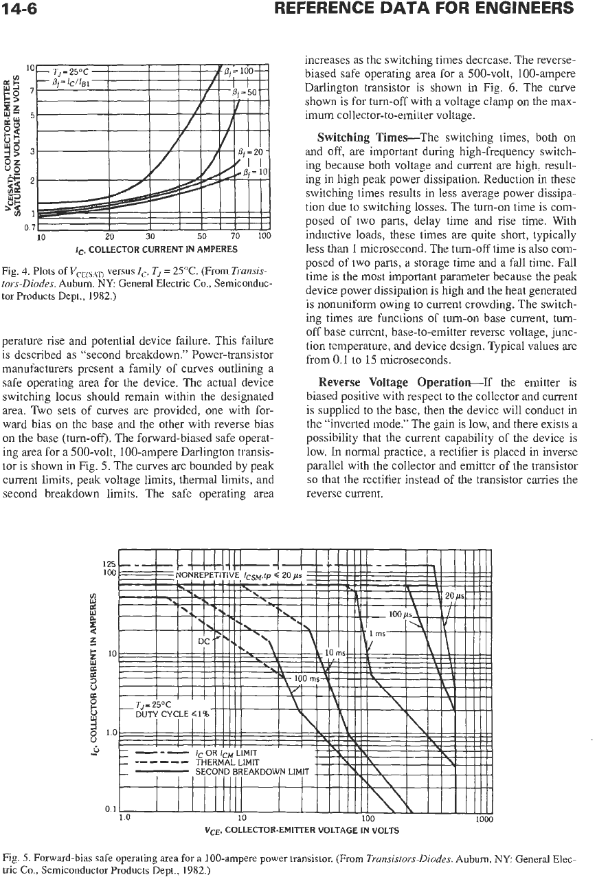
Fig.
4.
Plots of
V,,,,,,
versus
I,,
TJ
=
25°C. (From
Trunsis-
tors-Diodes.
Auburn,
NY
General Electric
Co.,
Semiconduc-
tor Products Dept., 1982.)
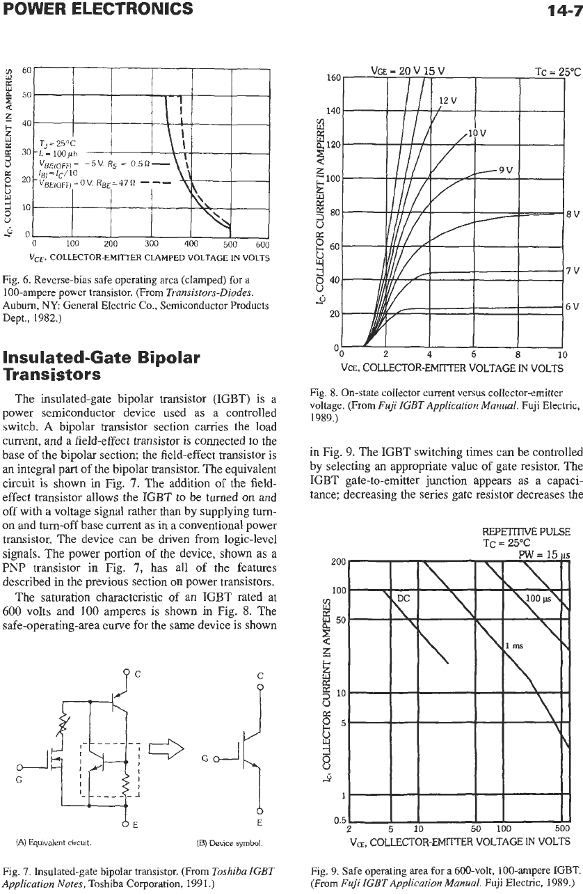
perature rise and potential device failure. This failure
is described as “second breakdown.” Power-transistor
manufacturers present a family of curves outlining a
safe operating area for the device. The actual device
switching locus should remain within the designated
area. Two sets
of
curves are provided, one with for-
ward bias on the base and the other with reverse bias
on the base (turn-off). The forward-biased safe operat-
ing area for a 500-volt, 100-ampere Darlington transis-
tor is shown in Fig.
5.
The curves are bounded by peak
current limits, peak voltage limits, thermal limits, and
second breakdown limits. The safe operating area
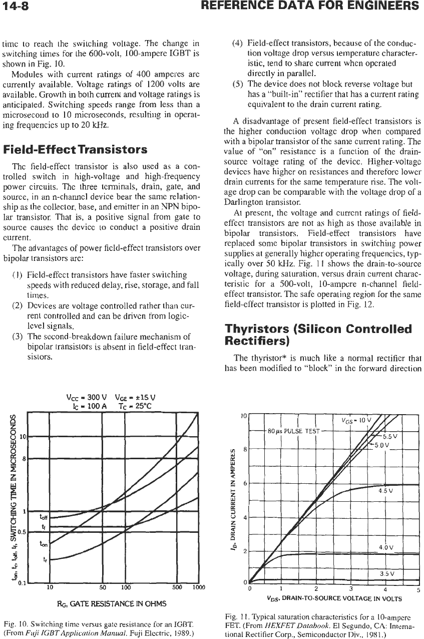
z
increases as the switching times decrease. The reverse-
biased safe operating area for a 500-volt, 100-ampere
Darlington transistor is shown
in
Fig.
6.
The curve
shown is for
turn-off
with a voltage clamp
on
the max-
imum collector-to-emitter voltage.
Switching Times-The switching times, both on
and
off,
are
important during high-frequency switch-
ing because both voltage and current are high, result-
ing in high peak power dissipation. Reduction in these
switching times results in less average power dissipa-
tion due
to
switching losses. The turn-on time is com-
posed of two parts, delay time and rise time. With
inductive loads, these times
are
quite short, typically
less than
1
microsecond. The
turn-off
time is also com-
125
100
10
0
1
10
10
100
1000
0
VCE.
COLLECTOR-EMITTER VOLTAGE IN VOLTS
Fig.
5.
Forward-bias safe operating area for a 100-ampere power transistor. (From
Transistors-Diodes.
Auburn,
NY General
Elec-
tric
Co.,
Semiconductor Products Dept., 1982.)
POWER
ELECTRONICS
I
I
I I
I
1
14-7
0
100
200
300
400
500
600
VCE.
COLLECTOR-EMITTER CLAMPED VOLTAGE
IN
VOLTS
Fig. 6. Reverse-bias
safe
operating area (clamped) for a
100-ampere
power
transistor. (From
Transistors-Diodes.
Auburn,
NY
General Electric Co., Semiconductor Products
Dept., 1982.)
Insulated-Gate Bipolar
Transistors
The insulated-gate bipolar transistor (IGBT) is a
power semiconductor device used as a controlled
switch.
A
bipolar transistor section carries the load
current, and
a
field-effect transistor is connected
to
the
base of the bipolar section; the field-effect transistor is
an integral part
of
the bipolar transistor. The equivalent
circuit is shown in Fig.
7.
The addition of the field-
effect transistor allows the IGBT to be turned
on
and
off
with a voltage signal rather than by supplying
turn-
on
and
turn-off
base current as in a conventional power
transistor. The device can be driven from logic-level
signals. The power portion
of
the device,
shown
as a
PNP
transistor in Fig.
7,
has all of the features
described
in
the previous section
on
power transistors.
The saturation characteristic of
an
IGBT rated at
600
volts and
100
amperes
is
shown in Fig.
8.
The
safe-operating-area curve for the same device is shown
le
I
I
I
J
(A)
Equivalent circuit.
(B) Device
symbol.
Fig.
7.
Insulated-gate bipolar transistor. (From
Toshiba IGBT
Application
Notes,
Toshiba Corporation, 1991.)
VCE, COLLECTOR-EMI7TER VOLTAGE
IN
VOLTS
Fig. %On-state collector current versus collector-emitter
voltage. (From
Fuji IGBTApplication Manual.
Fuji
Electric,
1989.)
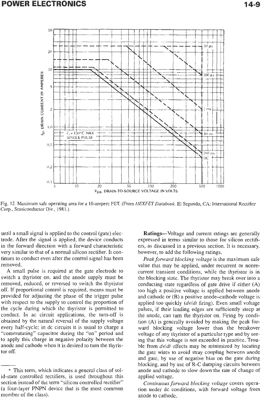
in Fig.
9.
The IGBT switching times can be controlled
by selecting an appropriate value
of
gate resistor. The
IGBT gate-to-emitter junction appears as a capaci-
tance; decreasing the series gate resistor decreases the
REPETITIVEPULSE
TC
=
25°C
VE, COLLECTOR-EMITTER VOLTAGE
IN
VOLTS
Fig.
9.
Safe operating area
for
a 600-volt, 100-ampere IGBT.
(From
Fuji
IGBTApplication Manual.
Fuji Electric, 1989.)
14-8
REFERENCE DATA FOR ENGINEERS
time to reach the switching voltage. The change in
switching times for the 600-volt, 100-ampere IGBT is
shown in Fig. 10.
Modules with current ratings of
400
amperes
are
currently available. Voltage ratings of 1200 volts are
available. Growth
in
both current and voltage ratings is
anticipated. Switching speeds range from less than a
microsecond to
10
microseconds, resulting in operat-
ing frequencies up to
20
kHz.
Field-Effect Transistors
The field-effect transistor is also used as a con-
trolled switch in high-voltage and high-frequency
power circuits. The three terminals, drain, gate, and
source, in an n-channel device bear the same relation-
ship as the collector, base, and emitter in an
NPN
bipo-
lar
transistor. That is, a positive signal from gate to
source causes the device to conduct a positive drain
current.
The advantages of power field-effect transistors over
bipolar transistors are:
(1)
Field-effect transistors have faster switching
speeds with reduced delay, rise, storage, and fall
times.
rent controlled and can be driven from logic-
level signals.
(3)
The second-breakdown failure mechanism of
bipolar transistors is absent in field-effect tran-
sistors.
(2)
Devices are voltage controlled rather than cur-
(4)
Field-effect transistors, because
of
the conduc-
tion voltage drop versus temperature character-
istic, tend to share current when operated
directly in parallel.
(5)
The device does not block reverse voltage but
has a “built-in” rectifier that has a current rating
equivalent
to
the drain current rating.
A
disadvantage of present field-effect transistors is
the higher conduction voltage drop when compared
with a bipolar transistor of the same current rating. The
value of “on” resistance is a function of the drain-
source voltage rating of the device. Higher-voltage
devices have higher on resistances and therefore lower
drain currents for the same temperature rise. The volt-
age drop can be comparable with the voltage drop of
a
Darlington transistor.
At
present, the voltage and current ratings of field-
effect transistors are not as high as those available
in
bipolar transistors. Field-effect transistors have
replaced some bipolar transistors in switching power
supplies at generally higher operating frequencies, typ-
ically over
50
kHz.
Fig. 11 shows the drain-to-source
voltage, during saturation, versus drain current charac-
teristic for a 500-volt, 10-ampere n-channel field-
effect transistor. The safe operating region for the same
field-effect transistor is plotted in Fig. 12.
Thyristors (Silicon Controlled
Rectifiers)
The thyristor* is much like a normal rectifier that
has been modified to “block” in the forward direction
RG,
GATE
RESISTANCE
IN
OHMS
VD~.
DRAIN-TO-SOURCE
VOLTAGE
1N
VOLTS
Fig.
11.
Typical saturation characteristics for a 10-ampere
FET.
(From
HEXFETDatabook.
El Segundo,
CA
Intema-
tional Rectifier
Corp.,
Semiconductor Div., 1981
.)
Fig.
10.
Switching time versus gate resistance for an
IGBT.
(From
Fuji
IGBTApplication
Manual.
Fuji Electric, 1989.)
POWER
ELECTRONICS
14-9
Fig.
12.
Maximum safe operating area
for
a 10-ampere
FET.
(From
HEXFETDutubook.
El
Segundo,
CA
International
Corp.,
Semiconductor
Div.,
1981.)
Rectifier
until a small signal is applied to the control (gate) elec-
trode. After the signal is applied, the device conducts
in the forward direction with a forward characteristic
very similar
to
that of a normal silicon rectifier. It con-
tinues
to
conduct even after the control signal has been
removed.
A
small pulse is required at the gate electrode to
switch a thyristor on, and the anode supply must be
removed, reduced, or reversed to switch the thyristor
off.
If
proportional control is required, means must be
provided for adjusting the phase of the trigger pulse
with respect to the supply to control the proportion of
the cycle during which the thyristor is permitted to
conduct. In ac circuit applications, the turn-off is
obtained by the natural reversal of the supply voltage
every half-cycle; in dc circuits it is
usual
to charge a
“commutating” capacitor during the
“on”
period and
to apply this charge in negative polarity between the
anode and cathode when it is desired to turn the thyris-
tor
off.
*
This term, which indicates a general class of sol-
id-state controlled rectifiers, is used throughout this
section instead of the term “silicon controlled rectifier”
(a four-layer
PNPN
device that is the most common
member of the class).
Ratings-Voltage and current ratings are generally
expressed
in
terms similar to those for silicon rectifi-
ers, as discussed in a previous section. It is necessary,
however, to add the following ratings.
Peak forward blocking voltage
is the maximum safe
value that may be applied, under recurrent or nonre-
current transient conditions, while the thyristor is in
the blocking state. The thyristor may break over into a
conducting state regardless
of
gate drive if either
(A)
too high a positive voltage is applied between anode
and cathode or
(B)
a positive anode-cathode voltage is
applied too quickly
(dvidt
firing). Even small voltage
pulses, if their leading edges are sufficiently steep at
the anode, can
turn
the thyristor on. Firing by condi-
tion
(A)
is generally avoided by making the peak for-
ward blocking voltage lower than the breakover
voltage
of
any thyristor
of
a particular type and by see-
ing that
this
voltage is
not
exceeded in practice.
Trou-
ble
from
dvidt
effects may be minimized by locating
the gate wires
to
avoid stray coupling between anode
and gate, by use of negative bias on the gate during
blocking, and by use
of
R-C
damping circuits between
anode and cathode
to
slow down the rate of change of
applied voltage.
Continuous forward blocking voltage
covers opera-
tion under dc conditions, with forward voltage from
anode to cathode.
14-1
0
REFERENCE
DATA
FOR ENGINEERS
Peak forward gate voltage
is quoted for the anode
positive with respect to the cathode and for the anode
negative with respect to the cathode. The voltage rat-
ing is quite low in the latter case (typically
0.25
V),
since the reverse voltage rating is reduced by forward
gate current.
Peak reverse gate voltage
is generally the same
whether the anode is positive or negative with respect
to the cathode.
Peak forward gate current
involves several factors.
Forward gate impedance is
a
finite value subject to
quite large variations between samples and over a tem-
perature range. It is usually necessary to plot a load
line on the gate current-voltage characteristics
to
determine the gate current that may flow due to a given
external gate voltage and source resistance. Care must
be taken that the rating is not exceeded with all known
spreads of gate-cathode characteristic and temperature.
Gate dissipation
is generally given
in
terms both of
average rating and of peak rating.
Characteristics-Characteristics of the thyristor
important for circuit design are as follows:
Leakage currents
are specified for both forward and
reverse blocking, at maximum applied voltage and at
maximum rated temperature. Although these currents
are
low in comparison with forward conducting cur-
rents and can be neglected in assessing power losses,
they must be taken into account in certain circum-
stances.
An
example would be
a
circuit in which a
capacitor
is
slowly charged from an external source
and then suddenly discharged through a thyristor into a
second circuit
(as
in pulse modulators); the capacitor
charging operation may be affected by the amount of
forward leakage current conducted by the thyristor in
its blocking state.
Holding current
is the minimum anode-cathode
current that will keep the thyristor conducting after it
has been switched on.
In
some applications,
a
thyristor
with
a
high holding current is wanted
so
that it can be
turned
off
easily without the need for reducing the
anode current to a very low level.
In
other applications,
where
a
low load current is normal, it might be desir-
able to have
a
low holding current to ensure that the
thyristor latches on reliably with light loading.
Forward voltage drop
is important
in
assessing
power
loss.
The
same methods of assessing power
loss
in terms
of
the forward current-voltage characteristic
apply as in the case of silicon rectifiers. It is impracti-
cable to measure the junction temperature under work-
ing conditions, and therefore the manufacturers list
maximum values of stud
or
case temperature related to
the forward current. This relationship is expressed in
the form of a graph,
as
shown in Fig.
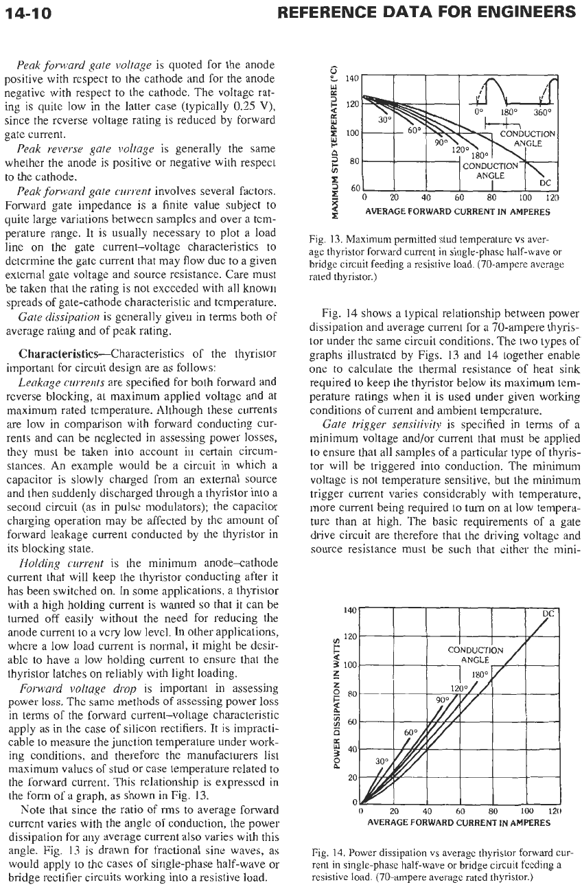
13.
Note that since the ratio of rms
to
average forward
current varies with the angle of conduction, the power
dissipation for any average current also varies with this
angle. Fig.
13
is
drawn for fractional sine waves,
as
would apply to the cases of single-phase half-wave or
bridge rectifier circuits working into a resistive load.
-
3
AVERAGE FORWARD CURRENT
IN
AMPERES
Fig.
13.
Maximum permitted stud temperature vs aver-
age thyristor forward current in single-phase half-wave or
bridge circuit feeding
a
resistive load. (70-ampere average
rated thyristor.)
Fig.
14
shows a typical relationship between power
dissipation and average current for
a
70-ampere thyris-
tor under the same circuit conditions. The two types of
graphs illustrated by Figs.
13
and
14
together enable
one
to
calculate the thermal resistance of heat sink
required to keep the thyristor below its maximum tem-
perature ratings when it
is
used under given working
conditions of current and ambient temperature.
Gate trigger sensitivity
is specified
in
terms of
a
minimum voltage and/or current that must be applied
to ensure that all samples of a particular type of thyris-
tor will be triggered into conduction. The minimum
voltage is not temperature sensitive, but the minimum
trigger current varies considerably with temperature,
more current being required
to
turn
on at low tempera-
ture than at high. The basic requirements of
a
gate
drive circuit are therefore that the driving voltage and
source resistance must be such that either the mini-
140
rr,
120
3
100
z
5
2
B
3
40
2
z
80
3
60
B
20
0
0
20
40
60
80
100
120
AVERAGE FORWARD CURRENT
IN
AMPERES
Fig.
14.
Power
dissipation vs average thyristor
forward
cur-
rent in single-phase half-wave or bridge circuit feeding a
resistive load. (70-ampere average rated thyristor.)
14-1
1
mum voltage or the minimum current (or both) is
exceeded but that the rated gate dissipation is not
exceeded.
Switching
times
of importance are the turn-on and
turn-off times, the latter generally being at least one
order of magnitude greater than the former. When a
gate signal is applied to the thyristor, there is a finite
delay time during which the anode current remains at
its normal blocking level; this is followed by a “rise
time” during which the anode current increases from
its blocking level
to
a value determined by the external
load circuit. Turn-on time is the sum of these two
times. For a given thyristor, the turn-on time is influ-
enced by the magnitude of gate drive, the load current
to be achieved, and, to a lesser extent, the applied
anode supply voltage. The time is reduced by high gate
drive, low load current, and high anode supply voltage.
Turn-off time is similarly composed
of
two individual
periods; the first is a storage time, analogous to that
obtained with a saturated transistor, and the second is a
recovery time. Forward voltage may not be reapplied
before the completion of both phases of the turn-off
process, or the thyristor may conduct load current
again. After this period, however, forward voltage may
be applied, and the thyristor will remain in its blocking
state provided that the rate of rise
of
anode voltage is
not allowed to exceed the specified maximum
dvidt,
as
already discussed.
Gate
Turn-Off
Thyristors-These devices
are
fab-
ricated to be able to turn off and interrupt the anode
current by extracting current from the gate-to-cathode
terminals. The ratio of controllable anode current to
gate current is from 3/1 to 5/1. However, the reverse
gate voltage is low, yielding a high power gain. These
thyristors
are
rated up
to
4500
volts and
2500
amperes.
MOS-Controlled Thyristors
The MOS-controlled thyristor is
a
four-layer, three-
junction semiconductor similar to the thyristor
described in the preceding section, except that an inte-
gral field-effect transistor has been added in parallel
with the anode and the anode gate. The equivalent cir-
cuit is shown in Fig.
15.
The addition of the field-effect
structures allows the device to be turned
on
and off by
a logic-level voltage signal. Reference
1
describes the
device structure and features. Devices in a TO-218
plastic package are available with ratings of
600
volts
and
50
amperes. Growth in voltage and current ratings
is anticipated. Higher-current modules have been fab-
ricated using selected lower-current devices operating
in parallel. Switching times are currently in the range
from
0.5
to 3 microseconds.
Triacs
A triac is a three-terminal ac semiconductor switch
that is triggered into conduction by a gate signal much
as a thyristor is. The triac was developed to provide a
P
Fig.
15.
Equivalent circuit
of
a
MOS-controlled thyristor.
single device that could control current flow in both
directions with the application of a gate signal. This
allowed for the replacement of two inverse-parallel
thyristors and the complex gate-drive circuit they
require with a single device that has a single gate.
The terms “anode” and “cathode” are not used;
instead, the power terminals
are
numbered
MT,
and
MT,. The gate terminal is associated with MT,. The
triggering characteristics are such that with MT, posi-
tive with respect to MT,, either positive or negative
gate current will trigger the device into conduction.
With MT, positive with respect to MT,, again either
positive or negative gate current will trigger the device
into conduction. However, positive gate current should
be used only if needed, because the gain is lower.
The other major difference from two inverse thyris-
tors is in the commutating
dvldt
rating. When two thy-
ristors are connected
in
inverse parallel and operating
with a lagging-power-factor load, one device ceases to
conduct, and the voltage rises
on
the previously con-
ducting device
in
the reverse or non-turn-on direction.
The other device sees a positive
dvldt
in the turn-on
direction, but it has had an entire half-cycle for turn-
off or commutation.
In
a triac, the only period for
tum-
off
occurs when the current goes through zero and
a
pulse of recovery current is conducted through the
device. The voltage rises to the circuit voltage level in
the turn-on direction very rapidly, and the device does
not have an entire half-cycle to regain its forward
blocking capability. A suitable
R-C
snubber is gener-
ally provided.
Triacs
are
available for standard ac voltages
(120,
240,
and some higher voltages) and up to
40-100
amperes operating at
50,
60,
or
400
hertz. The remain-
der
of
their ratings are consistent with thyristor ratings.