Middleton W.M. (ed.) Reference Data for Engineers: Radio, Electronics, Computer and Communications
Подождите немного. Документ загружается.

16-26
REFERENCE
DATA
FOR
ENGINEERS
107
106
105
104
103
102
10
1
10-1
io-*
1
1
10
100
1
,oO0
10,Ooo
1
oo,oO0
Frequency
(GHz)
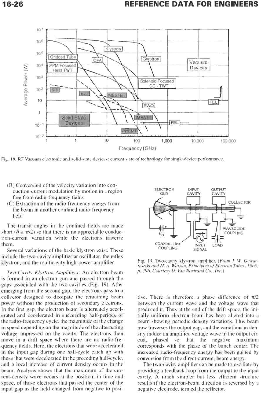
Fig.
18.
RF
Vacuum electronic and solid-state devices: current state
of
technology
for
single device performance.
(B)
Conversion of the velocity variation into con-
duction-current modulation by motion in a region
free from radio-frequency fields
(C) Extraction of the radio-frequency energy
from
the beam in another confined radio-frequency
field
The transit angles
in
the confined fields
are
made
short
(6
E
m/2)
so
that there is no appreciable conduc-
tion-current variation while the electrons traverse
them.
Several variations of the basic klystron exist.
These
include the two-cavity amplifier
or
oscillator, the reflex
klystron, and the multicavity high-power amplifier.
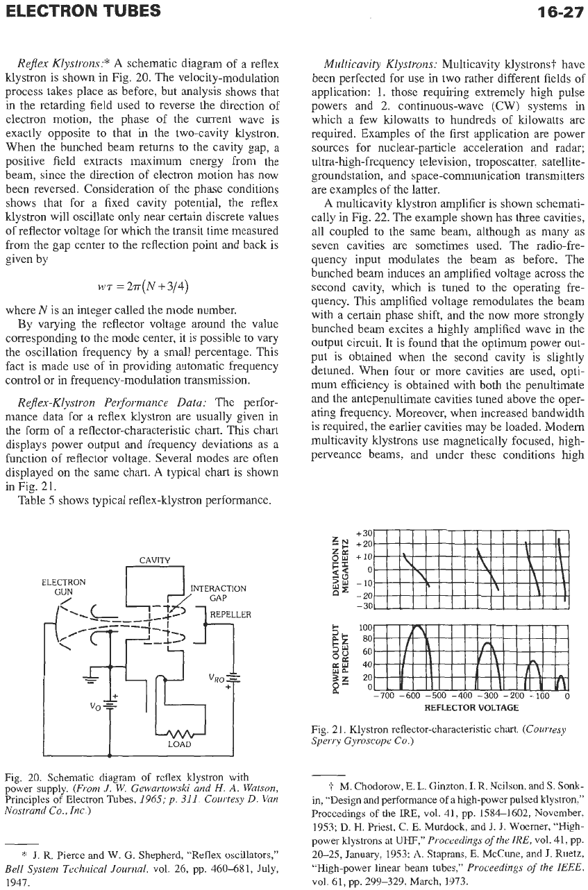
Two-CaviQ
Klystron
Amplifrers:
An electron
beam
is formed in an electron gun and passed through the
gaps associated with the two cavities (Fig.
19).
After
emerging from the second gap, the electrons pass to a
collector designed to dissipate the remaining beam
power without the production of secondary electrons.
In the first gap, the electron beam is alternately accel-
erated and decelerated in succeeding half-periods of
the radio-frequency cycle, the magnitude of the change
in speed depending on the magnitude of the alternating
voltage impressed on the cavity. The electrons then
move in a drift space where there are no radio-fre-
quency fields. Here, the electrons that were accelerated
in the input gap during one half-cycle catch up with
those that were decelerated in the preceding half-cycle,
and a local increase of current density occurs in the
beam. Analysis shows that the maximum of the cur-
rent-density wave occurs at the position, in time and
space, of those electrons that passed the center of the
input gap as the field changed from negative to posi-
ELECTRON
INPOT
OW
GUN CAVITY CAVITY
COAXIAL LINE
IN~
LOAD
COUPLING SIGNAL
Fig.
19.
Twocavity klystron amplifier.
(Fmm
J.
W. Gewar-
towski and
H.
A.
Watson, Principles
of
Electron Tubes,
1965;
p.
296.
Courtesy
D.
Van Nostrand
Co.,
Inc.)
tive. There is therefore a phase difference of
sc/2
between the current wave and the voltage wave that
produced it. Thus at the end of the
drift
space, the ini-
tially uniform electron beam has been altered into a
beam showing periodic density variations. This
beam
now traverses the output gap, and the variations in den-
sity induce an amplified voltage wave in the output cir-
cuit, phased
so
that the negative maximum
corresponds with the phase of the bunch center. The
increased radio-frequency energy has been gained by
conversion from the direct-current, beam energy.
The
two-cavity amplifier can
be
made to oscillate by
providing a feedback loop from the output to the input
cavity. A much simpler but less efficient structure
results if
the
electron-beam direction is reversed by a
negative electrode, termed the reflector.
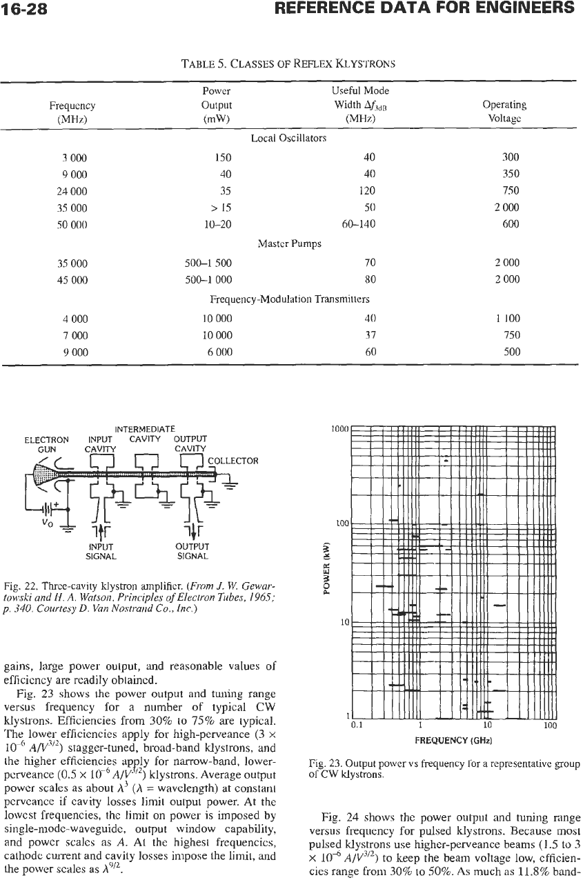
Reflex Klystrons:*
A
schematic diagram of a reflex
klystron is shown in Fig.
20.
The velocity-modulation
process takes place as before, but analysis shows that
in the retarding field used to reverse
the
direction of
electron motion, the phase of the current wave is
exactly opposite to that in the two-cavity klystron.
When the bunched beam returns to the cavity gap, a
positive field extracts maximum energy from the
beam, since the direction of electron motion has now
been reversed. Consideration of the phase conditions
shows that for a fixed cavity potential, the reflex
klystron will oscillate only near certain discrete values
of reflector voltage for which the transit time measured
from the gap center to the reflection point and back is
given by
WT
=
2r(N
+
3/4)
where
N
is an integer called the mode number.
By varying the reflector voltage around the value
corresponding to the mode center, it is possible to vary
the oscillation frequency by a small percentage. This
fact is made use of
in
providing automatic frequency
control or in frequency-modulation transmission.
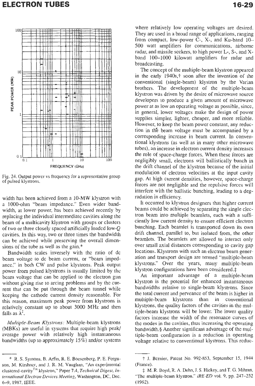
Refex-Klystron Performance Data:
The perfor-
mance data for a reflex klystron are usually given in
the form
of
a reflector-characteristic chart. This chart
displays power output and frequency deviations as a
function of reflector voltage. Several modes are often
displayed on the same chart.
A
typical chart is shown
in Fig.
21.
Table
5
shows typical reflex-klystron performance.
CAVITY
-
INTERACTION
’
GAP
Multicavity Klystrons:
Multicavity klystrons? have
been perfected for use in two rather different fields of
application:
1.
those requiring extremely high pulse
powers and
2.
continuous-wave (CW) systems in
which a few kilowatts to hundreds of kilowatts are
required. Examples of the first application
are
power
sources for nuclear-particle acceleration and radar;
ultra-high-frequency television, troposcatter, satellite-
groundstation, and space-communication transmitters
are examples of the latter.
A
multicavity klystron amplifier is shown schemati-
cally in Fig.
22.
The example shown has three cavities,
all coupled to the same beam, although as many as
seven cavities are sometimes used. The radio-fre-
quency input modulates the beam as before. The
bunched beam induces an amplified voltage across the
second cavity, which is tuned
to
the operating fre-
quency. This amplified voltage remodulates the beam
with a certain phase shift, and the now more strongly
bunched beam excites a highly amplified wave in the
output circuit. It is found that the optimum power out-
put is obtained when the second cavity is slightly
detuned. When four or more cavities are used, opti-
mum efficiency is obtained with both the penultimate
and the antepenultimate cavities tuned above the oper-
ating frequency. Moreover, when increased bandwidth
is required, the earlier cavities may be loaded. Modem
multicavity klystrons use magnetically focused, high-
perveance beams, and under these conditions high
+
30
+
20
-
30
5
100
3z
2;
-700
-600
-500
-400
-300
-200
-100
0
REFLECTOR VOLTAGE
2
Fig. 21, Klystron reflector-characteristic chart.
(Courtesj
Sperry Gyroscope
Co.)
Fig.
20.
Schematic diagram
of
reflex klystron with
power supply,
(From
J.
W.
Gewartowski and
H.
A.
Watson,
Principles of Electron
Tubes, 1965;
p.
311.
Courtesy
D.
Van
Nostrand
Co.,
Inc.)
*
J.
R.
Pierce and
W.
G.
Shepherd,
“Reflex
oscillators,”
Bell
System Technical Journal,
vol.
26,
pp. 460-681, July,
1947.
t
M.
Chodorow,
E.
L.
Ginzton,
I.
R.
Neilson, and
S.
So&-
in,
“Design and perfonnance of ahigh-power pulsed klystron,”
Proceedings
of
the
IRE,
vol.
41,
pp. 15861602, November,
1953;
D.
H. Priest, C. E. Murdock, and
J.
J.
Woemer, “High-
power klystrons at
UHF,”
Proceedings
of
the
IRE,
vol.
41,
pp.
20-25,
January, 1953; A. Staprans,
E.
McCune,
and
J.
Ruetz,
“High-power
linear
beam tubes,”
Proceedings
of
the
IEEE,
VO~.
61, pp. 299-329,
March,
1973.
16-28
REFERENCE
DATA
FOR
ENGINEERS
TABLE
5.
CLASSES
OF
REFLEX
KLYSTRONS
Power
output
(mW)
Useful
Mode
Width AhdB
(MW
Operating
Voltage
3
000
9
000
24
000
35
000
50
000
35
000
45
000
4
000
7
000
9
000
Local Oscillators
150
40
40
40
35
120
>
15
50
10-20 60-140
Master Pumps
500-1
500
70
500-1 000
80
Frequency-Modulation Transmitters
10
000
40
10
000
37
6
000
60
300
350
750
2
000
600
2
000
2
000
1100
750
500
INTERMEDIATE
ELECTRON INPUT CAVITY OUTPUT
GUN CAVITY CAVITY
COLLEC
INPUT OUTPUT
SIGNAL SIGNAL
:TOR
Fig. 22. Three-cavity klystron amplifier. (From
J.
W. Gewar-
towski and
H.
A.
Watson, Principles
of
Electron Tubes,
1965;
p.
340.
Courtesy
D.
Van
Nostrand
Co.,
Inc.)
gains, large power output, and reasonable values of
efficiency are readily obtained.
Fig.
23
shows the power output and
tuning
range
versus frequency for a number of typical
CW
klystrons. Efficiencies from
30%
to
75%
are
typical.
The lower efficiencies apply for high-perveance
(3
x
A/V3”)
stagger-tuned, broad-band klystrons, and
the higher efficiencies ap ly for narrow-band, lower-
power scales as about
A3 (A
=
wavelength) at constant
perveance if cavity losses limit output power.
At
the
lowest frequencies, the limit
on
power is imposed by
single-mode-waveguide, output window capability,
and power scales
as
A.
At
the highest frequencies,
cathode current and cavity losses impose the limit, and
the power scales as
A9’2.
perveance
(0.5
x
A/V
82
)
klystrons. Average
output
1000
100
-
k
g
8
10
1
0.1
1
10
100
FREQUENCY
(GHz)
Fig. 23.
Output
power
of
CW klystrons.
vs
frequency for a representative group
Fig.
24
shows the power output and tuning range
versus frequency for pulsed klystrons. Because most
pulsed klystrons use higher-perveance beams
(1.5
to
3
x
A/V3I2)
to keep the beam voltage low, efficien-
cies range from
30%
to
50%.
As
much
as
11.8% band-
16-29
Fig.
24.
Output power
vs
frequency for a representative group
of
pulsed
klystrons.
width has been achieved from a
10-MW
klystron with
a
1000-ohm
“beam impedance.” Even wider band-
width, at lower power, has been achieved recently by
replacing the individual intermediate cavities along the
beam of a multicavity klystron with groups or clusters
of two or three closely spaced artificially loaded low-Q
cavities.
In
this
way, two or three times the bandwidth
can be achieved while preserving the overall dimen-
sions of
the
tube as well as the gain.*
Bandwidth scales inversely with the ratio of dc
beam voltage to dc beam current, or “beam imped-
ance,” in both
CW
and pulse klystrons. Peak output
power from pulsed klystrons is usually limited by the
beam voltage that can be applied to the electron gun
without giving rise
to
arcing problems and by the cur-
rent that can be put through the beam tunnel while
keeping the cathode current density reasonable. For
this reason, maximum peak power from klystrons is
relatively constant up
to
about
3000
MHz
and then
falls as
h2.
Multiple-Beam
Klystrons:
Multiple-beam
klystrons
(MBKs)
are useful in systems that require high peak/
average power with relatively high instantaneous
bandwidths (up
to
approximately
15%)
and/or systems
*
R.
S.
Symons,
B.
Arfin,
R.
E. Boesenberg, P. E. Fergu-
son,
M.
Kirshner, and
J.
R.
M.
Vaughan,
“An
experimental
clustered-cavityTm klystron,” Paper 7.4,
Technical Digest, In-
ternational Electron Devices Meeting,
Washington, DC, Dec.
6-9,1987, IEEE.
where relatively low operating voltages are desired.
They are used in a broad range
of
applications, ranging
from compact, low-power
C-,
X-,
and Ku-band
10-
500
watt amplifiers for communications, airborne
radar, and missile seekers, to high power
L-,
S-,
and
X-
band
100-1000
kilowatt amplifiers for radar and
broadcasting.
The concept of the multiple-beam klystron appeared
in the early
1940s,t
soon
after the invention of the
conventional (single-beam) klystron by the Varian
brothers. The development of the multiple-beam
klystron was driven by the desire of microwave source
developers to produce a given amount of microwave
power at as low an operating voltage as possible, since,
in general, lower voltages make the design
of
power
supplies simpler, lighter, cheaper, and more reliable.
However, to keep the beam power constant, any reduc-
tion in thE beam voltage must be accompanied by a
corresponding increase in beam current.
In
conven-
tional klystrons (as well as in many other microwave
tubes), an increase in electron current density increases
the role of space-charge forces. When these forces are
negligibly small, electrons will ballistically bunch in
the drift channel
of
the klystron because of the initial
modulation of electron velocities at the input cavity
gap. At high current densities, however, space-charge
forces are not negligible and the repulsive forces will
interfere with the ballistic bunching, leading
to
a deg-
radation in efficiency.
It occurred to klystron designers that higher current
beams could be achieved by separating the single elec-
tron beam into multiple beamlets, each with a suffi-
ciently low current density to ensure efficient electron
bunching. Each beamlet is transported down its own
drift channel, parallel to, but isolated from, the other
beamlets. The beamlets are allowed to interact only
over small axial distances corresponding to cavity gap
locations. Klystrons with such an electron beam gener-
ation and transport design
are
termed “multiple-beam
klystrons.” Over the years, many multiple-beam
klystron configurations have been considered.$
An
important advantage of a multiple-beam
klystron
is
the potential for enhanced instantaneous
bandwidths relative to single-beam klystrons. Since
the total current and perveance of the beam is higher in
multiple-beam klystrons than in conventional
klystrons,
the
quality factors of the cavities in the mul-
tiple-beam klystrons will be lower. The lower quality
factors increase the width of the resonance curves of
the modes
in
the cavities,
thus
increasing
the
operating
bandwidth.$ Another significant advantage of the mul-
tiple-beam configuration
is
a reduction in operating
voltage relative to conventional klystrons. This reduc-
t
J.
Bemier, Patent
No.
992-853, September 15, 1944
(France).
8
M.
R.
Boyd,
R.
A.
Dehn,
J.
S.
Hickey, and
T.
G.
M~hran,
“The multiple-beam klystron,”
IRE-ED
vol.
9,
pp. 247-252
(1962).
tion in voltage can be illustrated by examining the
cases of a multiple-beam klystron and a single-beam
klystron
(SBK)
generating the same level of micro-
wave power with the following assumptions:
(i)
the
microperveance of a single beamlet in the multiple-
beam klystron is the same as the microperveance of a
whole beam in the single-beam klystron;
(ii)
the power
and efficiency
of
the multiple-beam and single-beam
klystrons are identical; and
(iii)
the electron current
density in both cases is limited by space-charge
effects. Under these assumptions, the voltage for the
multiple-beam klystron will scale as
v,,,
=
v,,,/N”/~,
where
N
is
number
of
beamlets.
In
addition, the total
length of the interaction region will scale as
Vi&,
and
so
the
reduced
voltage
also
leads to
a
more com-
pact device.
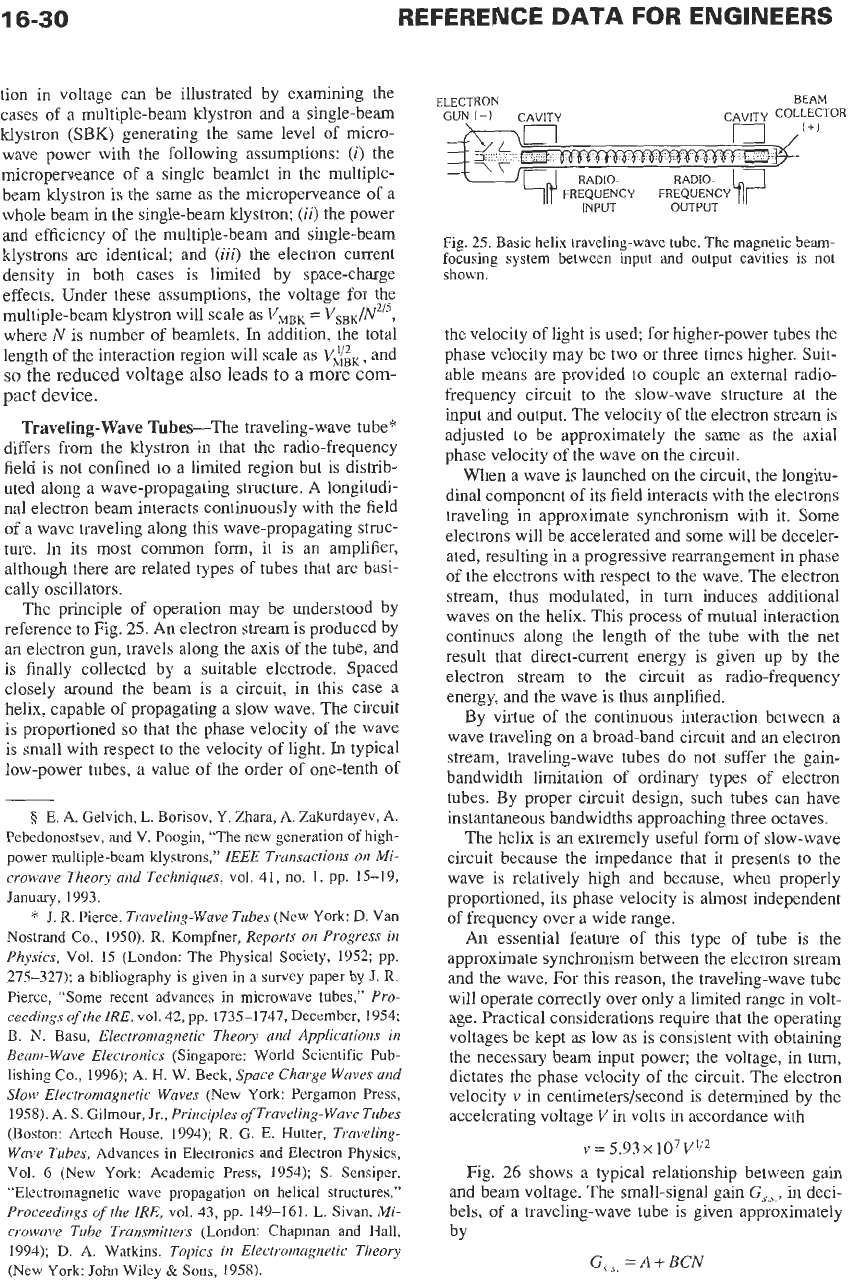
Traveling-Wave Tubes-The traveling-wave tube*
differs from the klystron in that the radio-frequency
field is not confined to a limited region but is distrib-
uted along a wave-propagating structure.
A
longitudi-
nal electron beam interacts continuously with the field
of
a wave traveling along this wave-propagating struc-
ture.
In
its most common form, it is an amplifier,
although there are related types of tubes that are basi-
cally oscillators.
The principle of operation may be understood by
reference
to
Fig.
25.
An
electron stream is produced by
an electron
gun,
travels along the axis of the tube, and
is finally collected by a suitable electrode. Spaced
closely around the beam is a circuit, in this case a
helix, capable of propagating a slow wave. The circuit
is proportioned
so
that the phase velocity of the wave
is small with respect to the velocity of light.
In
typical
low-power tubes, a value of the order of one-tenth
of
3
E.
A. Gelvich, L. Borisov, Y. Zhara, A. Zakurdayev, A.
Pebedonostsev, and
V.
Poogin, “The new generation of high-
power multiple-beam klystrons,”
IEEE
Transactions on Mi-
crowave Theory and Techniques,
vol.
41, no. l,
pp.
15-19,
January, 1993.
*
J.
R.
Pierce,
Traveling-Wave Tubes
(New
York:
D.
Van
Nostrand Co., 1950).
R.
Kompfner,
Reports on Progress in
Physics,
Vol.
15 (London: The Physical Society, 1952;
pp.
275-327); a bibliography is given in a survey paper by
J.
R.
Pierce, “Some recent advances in microwave tubes,”
Pro-
ceedings
of
the
IRE,
vol. 42,
pp.
1735-1747, December, 1954;
B.
N.
Basu,
Electromagnetic Theory and Applications in
Beam-Wave Electronics
(Singapore: World Scientific Pub-
lishing Co., 1996); A. H.
W.
Beck,
Space Charge Waves and
Slow
Electromagnetic Waves
(New York: Pergamon Press,
1958). A.
S.
Gilmour, Jr.,
Principles
of
Traveling-Wave Tubes
(Boston:
Artech
House,
1994);
R.
G.
E. Hutter,
Traveling-
Wave Tubes,
Advances in Electronics
and
Electron Physics,
Vol.
6
(New York: Academic
Press,
1954);
S.
Sensiper,
“Electromagnetic wave propagation on helical structures,”
Proceedings
of
the
IRE,
vol. 43,
pp.
149-161. L. Sivan,
Mi-
crowave Tube Transmitters
(London: Chapman and Hall,
1994);
D.
A. Watkins,
Topics in Electromagnetic Theoly
(New York:
John
Wiley
&
Sons,
1958).
ELECTRON BEAM
CAVITY
COLLECTOR
GUN
(-
CAVITY
(+I
Fig
25. Basic helix traveling-wave tube. The magnetic
bean-
focusing system between input
and
output cavities is not
shown
the velocity of light is used; for higher-power tubes the
phase velocity may be two or three times higher.
Suit-
able means are provided
to
couple an external radio-
frequency circuit to the slow-wave structure at the
input and output. The velocity of the electron stream is
adjusted
to
be approximately the same as the axial
phase velocity
of
the wave
on
the circuit.
When a wave
is
launched on the circuit, the longitu-
dinal component
of
its field interacts with the electrons
traveling in approximate synchronism with it. Some
electrons will be accelerated and some will be deceler-
ated, resulting
in
a progressive rearrangement
in
phase
of the electrons with respect
to
the wave. The electron
stream, thus modulated, in turn induces additional
waves
on
the helix. This process of mutual interaction
continues along the length of the tube with the net
result that direct-current energy is given up by the
electron stream
to
the circuit as radio-frequency
energy, and
the
wave is thus amplified.
By virtue
of
the continuous interaction between a
wave traveling
on
a broad-band circuit and an electron
stream, traveling-wave tubes do not suffer the gain-
bandwidth limitation
of
ordinary types of electron
tubes. By proper circuit design, such tubes can have
instantaneous bandwidths approaching three octaves.
The helix is an extremely useful
form
of slow-wave
circuit because the impedance that it presents to the
wave is relatively high and because, when properly
proportioned, its phase velocity is almost independent
of frequency over a wide range.
An essential feature of this type of tube is the
approximate synchronism between the electron stream
and the wave. For this reason, the traveling-wave tube
will operate correctly over only a limited
range
in
volt-
age. Practical considerations require that the operating
voltages be kept as low as is consistent with obtaining
the necessary beam input power; the voltage, in turn,
dictates the phase velocity
of
the circuit. The electron
velocity
v
in centimeters/second is determined by the
accelerating voltage
V
in volts
in
accordance with
v
=
5.93
x
107v’/*
Fig.
26
shows a typical relationship between gain
and beam voltage. The small-signal gain
G,
5,
in
deci-
bels,
of
a traveling-wave tube is given approximately
G,,
=A+BCN
by
ELECTRON TUBES
16-31
BEAM VOLTAGE
Fig.
26.
Traveling-wave tube gain
vs
accelerating voltage.
where
A
is the initial loss due to the establishment of the
modes on the helix and lies in the range from
-6
to
-9
decibels,
B
is
a
gain coefficient that accounts for the effect of
circuit attenuation and space charge,
C
is a gain parameter that depends
on
the imped-
ances of the circuit and the electron stream, and
N
is the number of active wavelengths in the tube.
and
where
I,
is the beam current,
Vo
is the beam voltage,
1,
is the free-space wavelength,
1
is the axial length of the helix,
v
is the phase velocity of the wave along the tube,
c
is the velocity of light.
and
The term
E2/(
mi
v)*
P
is
a
normalized wave impedance
that may be defined in
a
number of ways.
In
practice, the attenuation of the circuit will vary
along the tube, and consequently the gain per unit
length will not be constant. The total gain will be
a
summation
of
the
gains of various sections of the tube.
Commonly,
C
is of the order of 0.02 to 0.2 in helix
traveling-wave tubes; typical gains vary from
20
to 70
decibels, depending
on
the application. The gain in
a
tube designed to produce appreciable power will vary
somewhat with signal level when the beam voltage is
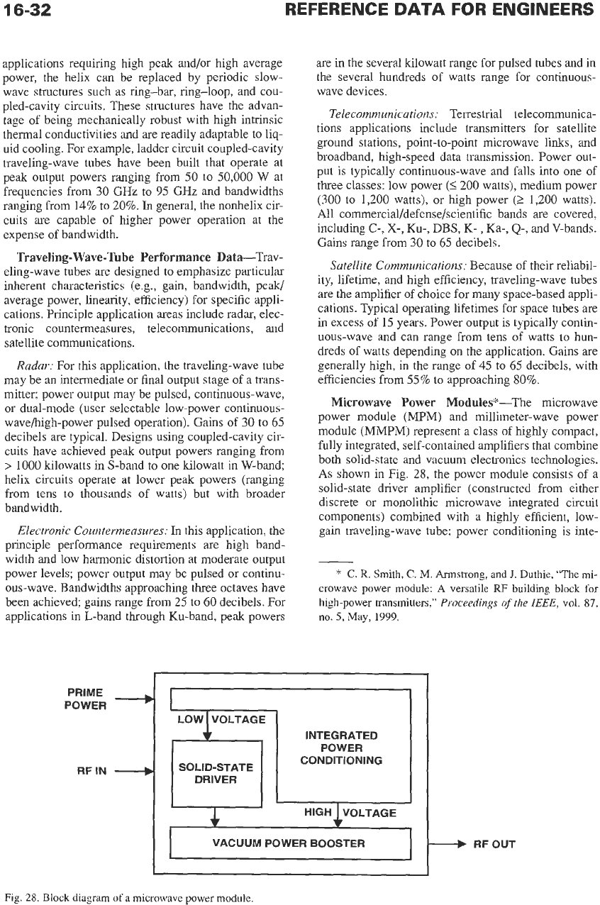
adjusted for optimum operation. Fig. 27 shows
a
typi-
cal characteristic.
To
restrain the physical size
of
the electron stream
as
it travels along the tube, it is necessary to provide
a
focusing field, either magnetic or electrostatic,
of
a
strength appropriate to overcome the space-charge
forces that would otherwise cause the beam to spread.
For
tubes requiring
a
strong confining field (in the
range of
0.5
to 2 tesla) and/or
a
high degree of spatial
field uniformity,
a
solenoid electromagnet is typically
used to generate the longitudinal magnetic field. Many
traveling-wave tube designs (e.g., for electronic war-
fare, communications, and airborne/space-based appli-
1
10
IO*
10
3
io4
105
RELATIVE
POWER
INPUT
Fig.
27.
Gain
of
traveling-wave tube
as
a function
of
input
level
and
beam voltage.
Eb,
<
Eb2
<
Eb3.
cations) require more modest bore fluxes in the range
of
0.2
to
0.5
tesla, allowing the use of periodic-perma-
nent-magnet
(PPM)
focusing. A
PPM
stack consists of
rings of permanent magnets with alternating axial
polarities separated by iron pole pieces and/or noncon-
ducting shims. Typically, the permanent magnets are
fabricated from
a
rare-earth compound of samarium-
cobalt or neodymium-iron-boron. The high-energy
products
([BH],,,
>
200 kilojoules/cubic meter) and
coercivities
(H,
>
100
amperes/meter) of these materi-
als enable amplifier designs with substantial weight
and size reductions compared
to
solenoid-focused sys-
tems
along
with improved efficiency and reliability
owing to the elimination of external electromagnet
power supplies.
After interacting with the fields in the slow-wave
circuit of the traveling-wave tube, the spent beam elec-
trons are collected in
an
electron collector. If the col-
lector is maintained at the same potential
as
the slow-
wave circuit, the kinetic energy of the electrons will be
dissipated in the walls of the collector as heat. How-
ever, if the collector is operated at
a
reduced
(depressed) potential relative to the slow-wave circuit,
much of the remaining energy in the beam can be
recovered by decelerating the electrons prior to collec-
tion, greatly enhancing the efficiency of the device.
In practice, the beam-wave interaction process
introduces
a
spread of velocities in the beam electrons;
for efficient collection, the collector must have multi-
ple electrodes (stages) maintained at
a
range of
depressed potentials to efficiently sort electrons travel-
ing at different velocities.
With
an optimized two- or
three-stage depressed collector, the efficiency of the
traveling-wave tube can be increased by
as
much
as
a
factor of two or three. For space-based applications,
where efficiency is critical,
a
traveling-wave tube may
use up to
a
five-stage depressed collector to achieve
narrow-band electronic efficiencies approaching
80%.
Helix traveling-wave circuits of the type shown
in
Fig.
25
are widely used in low- to medium-power
applications
(5
200 watts), where gain, bandwidth, and
efficiency are important performance criteria. For
applications requiring high peak and/or high average
power, the helix can be replaced by periodic slow-
wave structures such as ring-bar, ring-loop, and cou-
pled-cavity circuits. These structures have the advan-
tage of being mechanically robust with high intrinsic
thermal conductivities and are readily adaptable to liq-
uid cooling.
For
example, ladder circuit coupled-cavity
traveling-wave tubes have been built that operate at
peak output powers ranging from
50
to
50,000
W
at
frequencies from
30
GHz to
95
GHz and bandwidths
ranging from
14%
to
20%.
In
general, the nonhelix cir-
cuits are capable of higher power operation at the
expense of bandwidth.
Traveling-Wave-Tube Performance Data-Trav-
eling-wave tubes are designed to emphasize particular
inherent characteristics (e.g., gain, bandwidth, peak/
average power, linearity, efficiency) for specific appli-
cations. Principle application areas include radar, elec-
tronic countermeasures, telecommunications, and
satellite communications.
are
in the several kilowatt range for pulsed tubes and
in
the several hundreds of watts range for continuous-
wave devices.
Telecommunications:
Terrestrial telecommunica-
tions applications include transmitters for satellite
ground stations, point-to-point microwave links, and
broadband, high-speed data transmission. Power out-
put is typically continuous-wave and falls into one of
three classes: low power
(5
200
watts), medium power
(300
to
1,200
watts), or high power
(2
1,200
watts).
All
commercial/defense/scientific
bands are covered,
including
C-,
X-,
Ku-,
DBS, K-
,
Ka-,
Q-,
and V-bands.
Gains range from
30
to
65
decibels.
Satellite Communications:
Because of their reliabil-
ity, lifetime, and high efficiency, traveling-wave tubes
are the amplifier of choice for many space-based appli-
cations. Typical operating lifetimes for space tubes
are
in excess of
15
years. Power output is typically contin-
uous-wave and can range from tens of watts
to
hun-
dreds of watts depending
on
the application. Gains are
Radar:
For this application, the traveling-wave tube
may be an intermediate or final output stage of a trans-
generally high, in the range
of
45;o
65
decibels, with
efficiencies from
55%
to approaching
80%.
mitter; power output may be pulsed, continuous-wave,
or dual-mode (user selectable low-power continuous-
wavehigh-power pulsed operation). Gains of
30
to
65
decibels are typical. Designs using coupled-cavity cir-
cuits have achieved peak output powers ranging from
>
1000
kilowatts in S-band to one kilowatt in W-band;
helix circuits operate at lower peak powers (ranging
from tens to thousands
of
watts) but with broader
bandwidth.
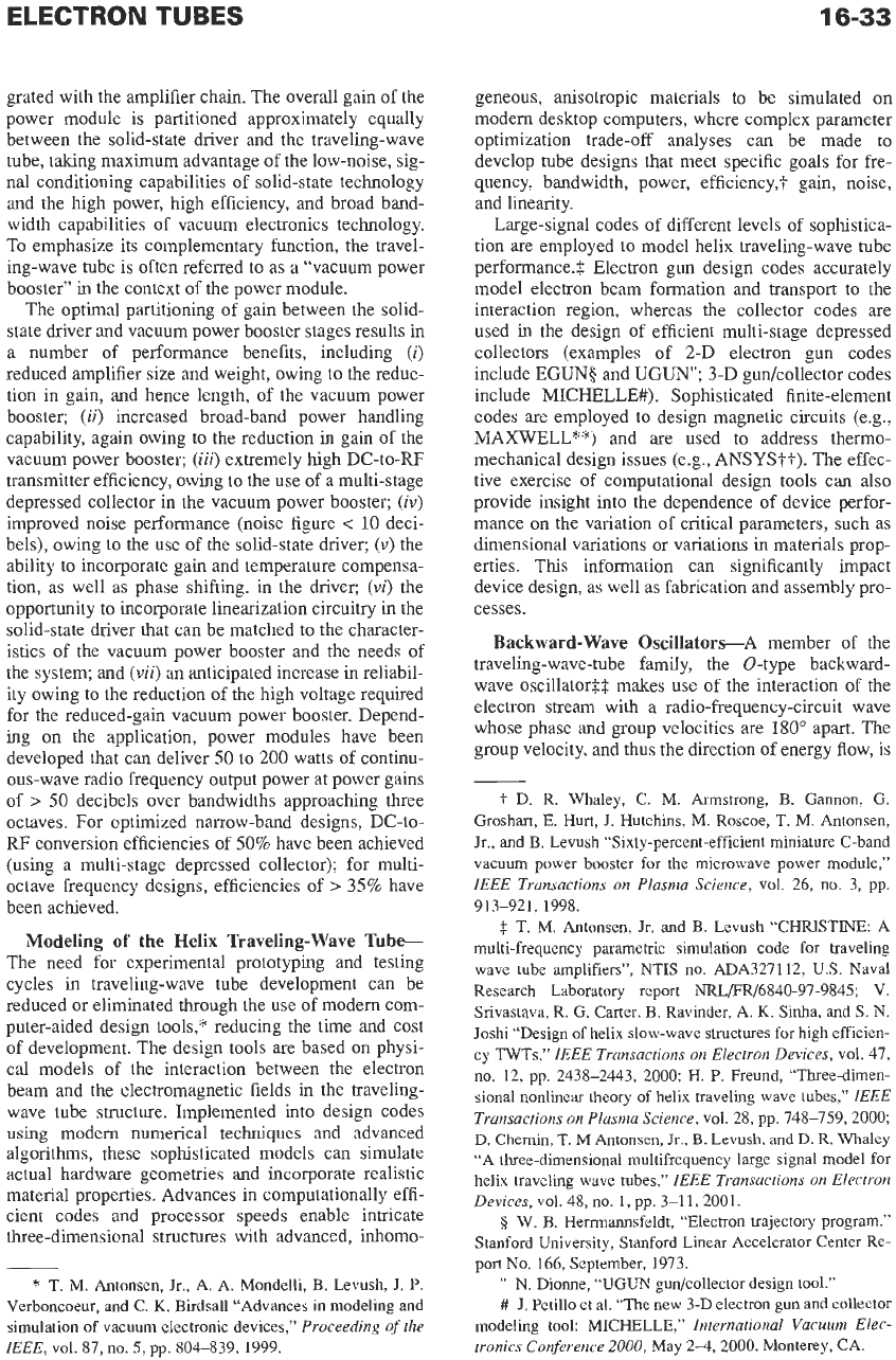
Microwave Power Modules*-The microwave
power module (MPM) and millimeter-wave power
module (MMPM) represent a class of highly compact,
fully integrated, self-contained amplifiers that combine
both solid-state and vacuum electronics technologies.
As
shown
in
Fig.
28,
the power module consists of a
solid-state driver amplifier (constructed from either
discrete or monolithic microwave integrated circuit
components) combined with a highly efficient, low-
Electronic Countermeasures:
In
this application, the
principle performance requirements are high band-
width and low harmonic distortion at moderate output
power levels; power output may be pulsed or continu-
ous-wave. Bandwidths approaching three octaves have
been achieved; gains range from
25
to
60
decibels. For
applications in L-band through Ku-band, peak powers
gain traveling-wave tube: power conditioning is inte-
-
*
C.
R.
Smith,
C.
M.
Armstrong,
and
J.
Duthie, “The mi-
crowave power
module:
A
versatile
RF
building
block for
high-power transmitters,”
Proceedings
of
the
IEEE,
vol.
87,
no.
5,
May,
1999.
PRIME
-
POWER
RFlN
INTEGRATED
POWER
CONDITIONING
SOLID-STATE
DRIVER
I
.
VACUUM POWER BOOSTER RFOUT
Fig.
28.
Block
diagram
of
a microwave
power module.
ELECTRON TUBES
16-33
grated with the amplifier chain. The overall gain of the
power module is partitioned approximately equally
between the solid-state driver and the traveling-wave
tube, taking maximum advantage of the low-noise, sig-
nal conditioning capabilities of solid-state technology
and the high power, high efficiency, and broad band-
width capabilities of vacuum electronics technology.
To emphasize its complementary function, the travel-
ing-wave tube is often referred
to
as a “vacuum power
booster” in the context of the power module.
The optimal partitioning of gain between the solid-
state driver and vacuum power booster stages results in
a
number of performance benefits, including
(i)
reduced amplifier size and weight, owing to
the
reduc-
tion
in
gain, and hence length, of the vacuum power
booster;
(ii)
increased broad-band power handling
capability, again owing
to
the reduction in gain of the
vacuum power booster;
(iii)
extremely high DC-to-RF
transmitter efficiency, owing to the use of a multi-stage
depressed collector in the vacuum power booster;
(iv)
improved noise performance (noise figure
c:
10
deci-
bels), owing
to
the use of the solid-state driver;
(v)
the
ability to incorporate gain and temperature compensa-
tion, as well as phase shifting, in the driver;
(vi)
the
opportunity to incorporate linearization circuitry in the
solid-state driver that can be matched to the character-
istics of the vacuum power booster and the needs of
the system; and
(vii)
an anticipated increase in reliabil-
ity owing to the reduction of the high voltage required
for the reduced-gain vacuum power booster. Depend-
ing
on
the application, power modules have been
developed that can deliver
50
to
200
watts of continu-
ous-wave radio frequency
output
power at power gains
of
>
50
decibels over bandwidths approaching three
octaves. For optimized narrow-band designs, DC-to-
RF
conversion efficiencies of
50%
have been achieved
(using a multi-stage depressed collector); for multi-
octave frequency designs, efficiencies of
>
35%
have
been achieved.
Modeling
of
the Helix Traveling-Wave
Tub+
The need for experimental prototyping and testing
cycles in traveling-wave tube development can be
reduced or eliminated through the use of modem com-
puter-aided design tools,* reducing the time and cost
of development. The design tools are based
on
physi-
cal models of the interaction between the electron
beam and the electromagnetic fields in the traveling-
wave tube structure. Implemented into design codes
using
modem
numerical
techniques
and advanced
algorithms, these sophisticated models can simulate
actual hardware geometries and incorporate realistic
material properties. Advances in computationally effi-
cient codes and processor speeds enable intricate
three-dimensional structures with advanced, inhomo-
*
T.
M.
Antonsen, Jr., A. A. Mondelli,
B.
Levush,
J.
P.
Verboncoeur, and C.
K.
Birdsall “Advances in modeling and
simulation of vacuum electronic devices,”
Proceeding of the
IEEE,
vol.
87,
no.
5,
pp. 806839,1999.
geneous, anisotropic materials to be simulated
on
modem desktop computers, where complex parameter
optimization trade-off analyses can be made to
develop tube designs that meet specific goals for fre-
quency, bandwidth, power, efficiency,? gain, noise,
and linearity.
Large-signal codes of different levels of sophistica-
tion
are
employed
to
model helix traveling-wave tube
performance.$ Electron gun design codes accurately
model electron beam formation and transport to the
interaction region, whereas the collector codes are
used in the design of efficient multi-stage depressed
collectors (examples of 2-D electron gun codes
include
EGUNC)
and
UGUN“;
3-D gun/collector codes
include MICHELLE#). Sophisticated finite-element
codes are employed to design magnetic circuits (e.g.,
MAXWELL**) and are used to address thermo-
mechanical design issues (e.g.,
ANSYSTt).
The effec-
tive exercise of computational design tools can also
provide insight into the dependence of device perfor-
mance
on
the variation of critical parameters, such as
dimensional variations or variations in materials prop-
erties.
This
information can significantly impact
device design,
as
well as fabrication and assembly pro-
cesses.
Backward-Wave Oscillators-A
member of the
traveling-wave-tube family, the 0-type backward-
wave oscillator$$ makes use of the interaction of the
electron stream with
a
radio-frequency-circuit wave
whose phase and group velocities
are
180”
apart. The
group velocity, and thus the direction of energy flow, is
t
D.
R.
Whaley, C. M. Armstrong, B. Gannon,
G.
Groshart,
E.
Hurt,
J.
Hutchins,
M.
Roscoe,
T.
M.
Antonsen,
Jr., and B. Levush “Sixty-percent-efficient miniature C-band
vacuum power booster for the microwave power module,”
IEEE Transactions on Plasma Science,
vol. 26, no. 3, pp.
913-921,1998.
f
T.
M.
Antonsen, Jr. and B. Levush “CHRISTINE: A
multi-frequency parametric simulation code for traveling
wave tube amplifiers”,
NTIS
no. ADA327112. U.S. Naval
Research Laboratory report NRL/FR/6840-97-9845; V.
Srivastava, R. G. Carter, B. Ravinder, A.
K.
Sinha, and
S.
N.
Joshi “Design of helix slow-wave structures for high efficien-
cy
TWTs,”
IEEE Transactions on Electron Devices,
vol. 41,
no. 12,
pp.
2438-2443,
2000;
H.
P.
Freund, “Three-dimen-
sional nonlinear theory
of
helix traveling wave tubes,”
IEEE
Transactions on Plasma Science,
vol.
28,
pp.
748-759,200&
D. Chemin,
T.
M
Antonsen,
Jr.,
B.
Levush, and
D.
R.
Whaley
“A three-dimensional multifrequency large signal model for
helix traveling wave tubes,”
IEEE Transactions on Electron
Devices,
vol. 48, no.
1,
pp. 3-1 1,2001.
Q
W.
B. Herrmannsfeldt, “Electron trajectory program.”
Stanford University, Stanford Linear Accelerator Center Re-
port
No.
166, September, 1973.
“
N.
Dionne,
“UGUN
gun/collector design tool.”
#
J.
Petillo et al. “The new 3-D electron gun and collector
modeling tool: MICHELLE,”
International Vacuum Elec-
tronics Conference
2000, May
2-4,
2000,
Monterey, CA.
16-34
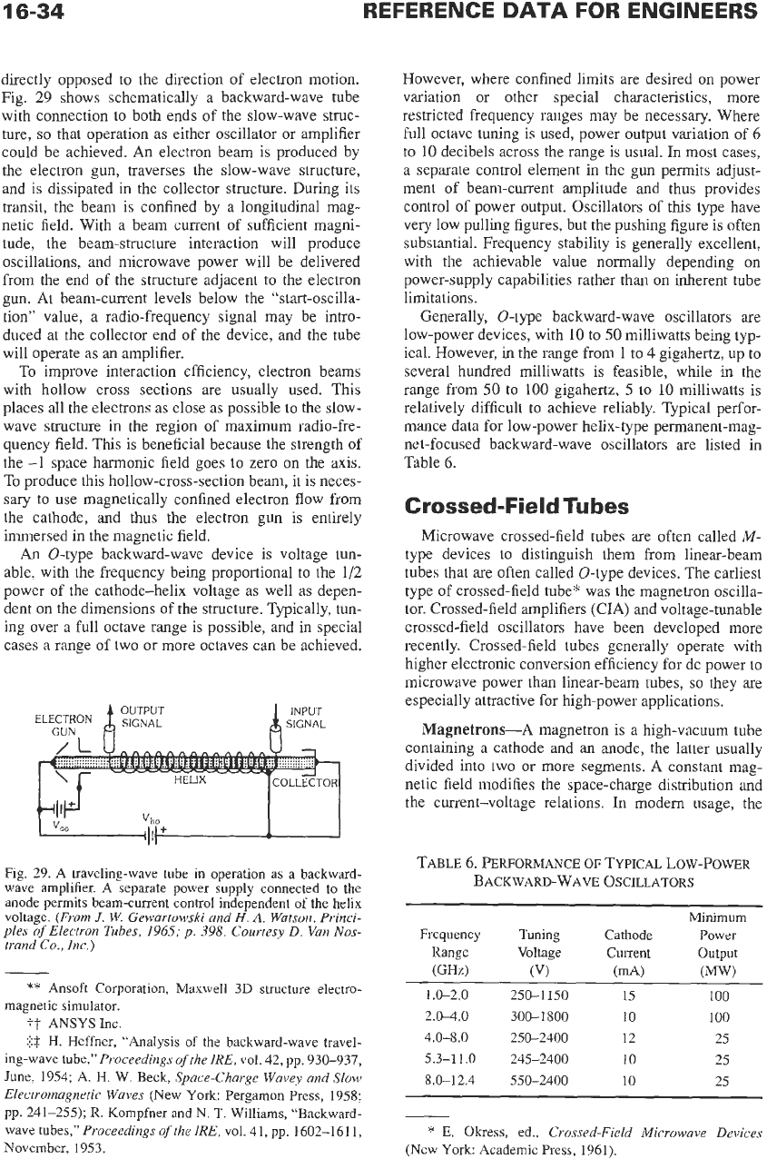
directly opposed
to
the direction of electron motion.
Fig. 29 shows schematically
a
backward-wave tube
with connection to both ends of the slow-wave struc-
ture,
so
that operation as either oscillator or amplifier
could be achieved. An electron beam is produced by
the electron gun, traverses the slow-wave structure,
and is dissipated in the collector structure. During its
transit, the beam is confined by a longitudinal mag-
netic field. With a beam current of sufficient magni-
tude, the beam-structure interaction will produce
oscillations, and microwave power will be delivered
from the end
of
the structure adjacent to the electron
gun. At beam-current levels below the “start-oscilla-
tion” value, a radio-frequency signal may be intro-
duced at the collector end of the device, and the tube
will operate as an amplifier.
To
improve interaction efficiency, electron beams
with hollow cross sections are usually used. This
places all the electrons as close as possible to the slow-
wave structure in the region of maximum radio-fre-
quency field. This is beneficial because the strength of
the
-1
space harmonic field goes to zero
on
the axis.
To
produce this hollow-cross-section beam, it is neces-
sary to use magnetically confined electron flow from
the cathode, and thus the electron gun is entirely
immersed in the magnetic field.
An
0-type backward-wave device
is
voltage tun-
able. with the frequency being proportional to the 1/2
power of the cathode-helix voltage as well
as
depen-
dent
on
the dimensions of the structure. Typically,
tun-
ing over
a
full octave range
is
possible, and in special
cases
a
range of two or more octaves can be achieved.
OUTPUT
ELECTRON
S~GNAL
GUN
a
INPUT
SIGNAL
A
Fig.
29.
A
traveling-wave tube in operation as a backward-
wave amplifier.
A
separate power
supply
connected
to
the
anode permits beam-current control independent
of
the
helix
voltage. (From
J.
W.
Gewartowski and
H.
A.
Watson, Princi-
ples
of
Electron Tubes,
1965;
p.
398.
Courtesy
D.
Van
Nos-
trund
Co.,
k.)
**
Ansoft Corporation, Maxwell
3D
structure electro-
magnetic simulator.
ft
ANSYSInC.
$$
H. Heffner, “Analysis
of
the
backward-wave travel-
ing-wave
tube,”
Proceedings
of
the IRE, vol.
42,
pp.
930-937,
June,
1954;
A.
H.
W. Beck, Space-Charge Wuvey and Slow
Electromagnetic Waves (New York: Pergamon Press,
1958;
pp.
241-255);
R.
Kompfner
and
N. T. Williams, “Backward-
wave tubes,” Proceedings
of
the IRE, vol.
41,
pp.
1602-161 1,
November,
1953.
However, where confined limits are desired
on
power
variation or other special characteristics, more
restricted frequency ranges may be necessary. Where
full octave tuning is used, power output variation of
6
to
10
decibels across the range
is
usual.
In
most cases,
a separate control element in the gun permits adjust-
ment of beam-current amplitude and thus provides
control of power output. Oscillators of
this
type have
very low pulling figures, but the pushing figure is often
substantial. Frequency stability is generally excellent,
with the achievable value normally depending
on
power-supply capabilities rather than
on
inherent tube
limitations.
Generally, 0-type backward-wave oscillators are
low-power devices, with
10
to
50
milliwatts being typ-
ical. However, in the range from
1
to
4
gigahertz, up
to
several hundred milliwatts is feasible, while
in
the
range from
50
to
100
gigahertz,
5
to 10 milliwatts is
relatively difficult to achieve reliably. Typical perfor-
mance data for low-power helix-type permanent-mag-
net-focused backward-wave oscillators are listed in
Table
6.
Crossed-Field
Tubes
Microwave crossed-field tubes are often called
M-
type devices to distinguish them from linear-beam
tubes that are often called 0-type devices. The earliest
type of crossed-field tube* was the magnetron oscilla-
tor. Crossed-field amplifiers (CIA) and voltage-tunable
crossed-field oscillators have been developed more
recently. Crossed-field tubes generally operate with
higher electronic conversion efficiency for dc power
to
microwave power than linear-beam tubes,
so
they are
especially attractive for high-power applications.
Magnetrons-A
magnetron is
a
high-vacuum tube
containing a cathode and an anode, the latter usually
divided into two or more segments. A constant mag-
netic field modifies the space-charge distribution and
the current-voltage relations. In modern usage, the
TABLE
6.
PERFORMAhTE
OF
TYPICAL LOW-POWER
BACKWARD-WAVE OSCILLATORS
Minimum
Frequency Tuning Cathode Power
Range
Voltage Current Output
(GHz)
(V)
(d)
(Mw)
1.0-2.0 250-1150
15 100
2.0-4.0 300-1800
10 100
4.0-8.0 250-2400
12 25
5.3-11.0 245-2400
10 25
8.0-12.4 550-2400
10 25
*
E.
Okress,
ed.,
Crossed-Field Microwave Devices
(New York: Academic
Press,
1961).
ELECTRON TUBES
16-35
term “magnetron” refers to the magnetron oscillator in
which the interaction of the electronic space charge
with the resonant system converts direct-current power
into alternating-current power, usually at microwave
frequencies.
Many forms of magnetrons have been made
in
the
past, and several kinds
of
operation have been
employed. The type of tube that is now almost univer-
sally employed is the multicavity magnetron generat-
ing traveling-wave oscillations. It possesses the
advantages of good efficiency at high frequencies,
capability of high outputs either in pulse or continu-
ous-wave operation, moderate magnetic-field require-
ments, and good stability
of
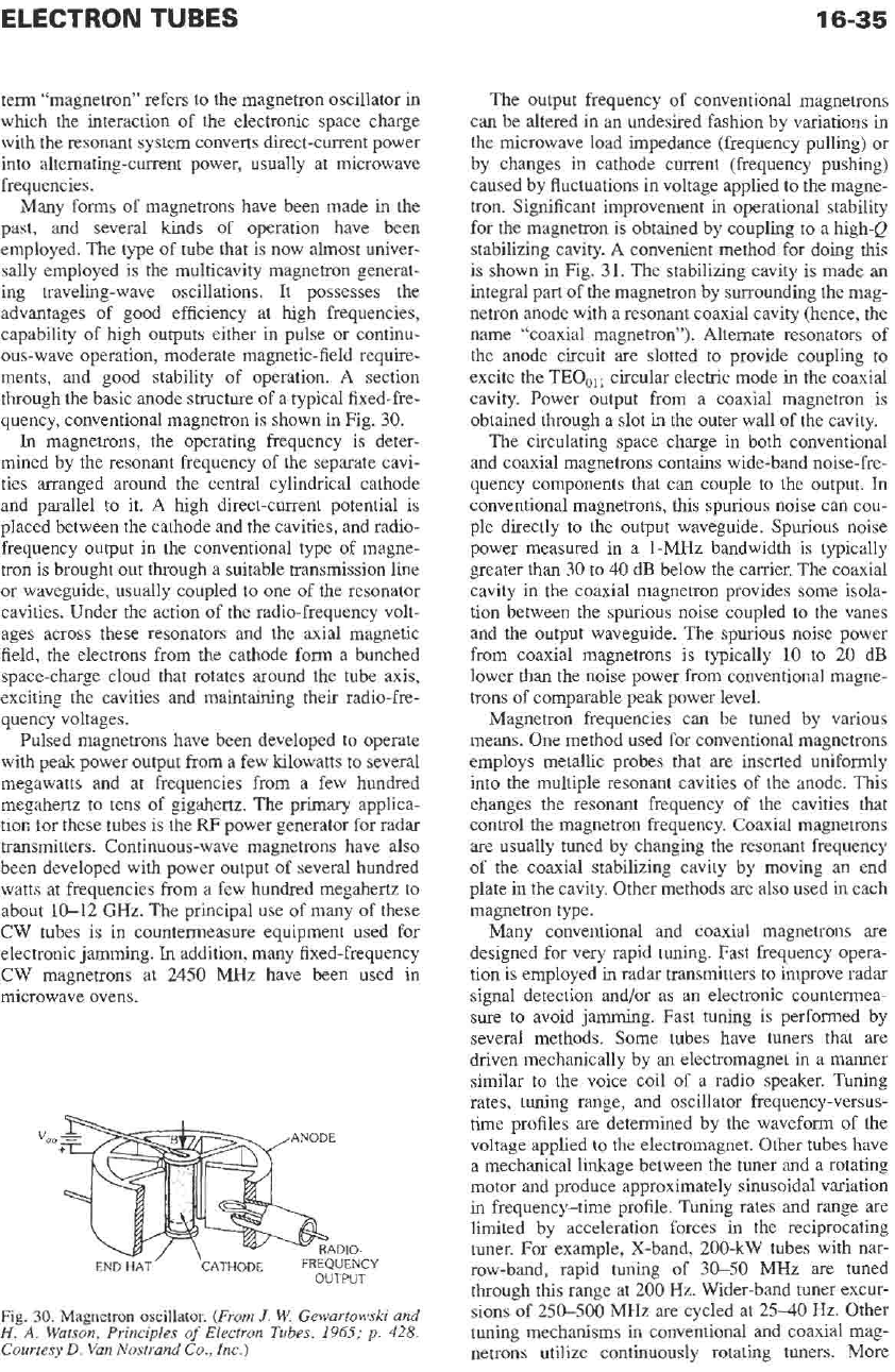
operation. A section
through the basic anode structure of a typical fixed-fre-
quency, conventional magnetron is shown in Fig.
30.
In magnetrons, the operating frequency is deter-
mined by the resonant frequency of
the
separate cavi-
ties arranged around the central cylindrical cathode
and parallel
to
it. A high direct-current potential is
placed between the cathode and the cavities, and radio-
frequency output in the conventional type
of
magne-
tron is brought out through a suitable transmission line
or waveguide, usually coupled
to
one of the resonator
cavities. Under the action of the radio-frequency volt-
ages across these resonators and the axial magnetic
field, the electrons from the cathode form a bunched
space-charge cloud that rotates around the tube axis,
exciting the cavities and maintaining their radio-fre-
quency voltages.
Pulsed magnetrons have been developed to operate
with peak power output from a few kilowatts to several
megawatts and at frequencies from a few hundred
megahertz to tens of gigahertz. The primary applica-
tion for these tubes is the
RF
power generator for radar
transmitters. Continuous-wave magnetrons have also
been developed with power output
of
several hundred
watts at frequencies from a few hundred megahertz
to
about 10-12 GHz. The principal use of many of these
CW tubes is in countermeasure equipment used for
electronic jamming.
In
addition, many fixed-frequency
CW magnetrons at 2450 MHz have been used in
microwave ovens.
IO
ENCY
OUTPUT
Fig.
30.
Magnetron oscillator.
(From
J.
W.
Gewartowski and
H.
A.
Watson, Principles
of
Electron Tubes,
1965;
p.
428.
Courtesy
D.
Van Nostrund
Co.,
Inc.)
The output frequency of conventional magnetrons
can be altered in an undesired fashion by variations
in
the microwave load impedance (frequency pulling) or
by changes in cathode current (frequency pushing)
caused by fluctuations in voltage applied
to
the magne-
tron. Significant improvement in operational stability
for the magnetron is obtained by coupling
to
a high-&
stabilizing cavity.
A
convenient method for doing
this
is shown in Fig.
31.
The stabilizing cavity is made an
integral part of the magnetron by surrounding the mag-
netron anode with a resonant coaxial cavity (hence, the
name “coaxial magnetron”). Alternate resonators
of
the anode circuit are slotted to provide coupling to
excite the TEO,,, circular electric mode
in
the coaxial
cavity. Power output from a coaxial magnetron is
obtained through a slot in the outer wall of the cavity.
The circulating space charge
in
both conventional
and coaxial magnetrons contains wide-band noise-fre-
quency components that can couple to the output. In
conventional magnetrons, this spurious noise can cou-
ple directly to the output waveguide. Spurious noise
power measured in a 1-MHz bandwidth is typically
greater than
30
to
40
dB
below the carrier. The coaxial
cavity in the coaxial magnetron provides some isola-
tion
between the spurious noise coupled to the vanes
and the output waveguide. The spurious noise power
from coaxial magnetrons is typically
10
to
20
dB
lower than the noise power from conventional magne-
trons of comparable peak power level.
Magnetron frequencies can be tuned by various
means. One method used for conventional magnetrons
employs metallic probes that
are
inserted uniformly
into the multiple resonant cavities of the anode. This
changes the resonant frequency of the cavities that
control the magnetron frequency. Coaxial magnetrons
are usually tuned by changing the resonant frequency
of the coaxial stabilizing cavity by moving an end
plate
in
the cavity. Other methods are also used
in
each
magnetron type.
Many conventional and coaxial magnetrons
are
designed for very rapid tuning. Fast frequency opera-
tion is employed in radar transmitters
to
improve radar
signal detection and/or as an electronic countermea-
sure
to
avoid jamming. Fast tuning is performed by
several methods. Some tubes have tuners that are
driven mechanically by an electromagnet in a manner
similar
to
the voice coil of a radio speaker. Tuning
rates, tuning range, and oscillator frequency-versus-
time profiles
are
determined by the waveform of the
voltage applied to the electromagnet. Other tubes have
a mechanical linkage between the tuner and a rotating
motor and produce approximately sinusoidal variation
in frequency-time profile. Tuning rates and range are
limited by acceleration forces
in
the reciprocating
tuner. For example, X-band, 200-kW tubes with
nar-
row-band, rapid tuning of
30-50
MHz are tuned
through
this
range at
200
Hz. Wider-band tuner excur-
sions of 250-500 MHz are cycled at 25-40 Hz. Other
tuning mechanisms
in
conventional and coaxial mag-
netrons utilize continuously rotating tuners. More