Middleton W.M. (ed.) Reference Data for Engineers: Radio, Electronics, Computer and Communications
Подождите немного. Документ загружается.

16-46
REFERENCE
DATA
FOR ENGINEERS
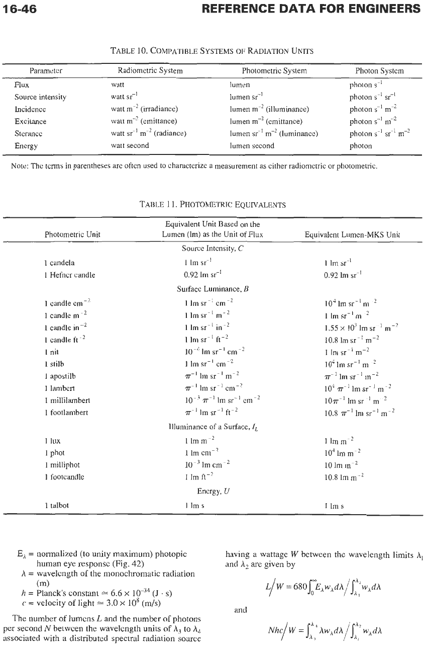
TABLE
10.
COMPATIBLE SYSTEMS
OF
RADIATION
UNITS
Parameter Radiometric Svstem Photometric Svstem Photon Svstem
Flux
watt
lumen photon
s-'
Source intensity watt sr-'
lumen sr-' photon
s-'
sr-'
Incidence watt m-' (irradiance)
lumen m-' (illuminance) photon
s-'
X2
Excitance watt
m-'
(emittance)
lumen
m-'
(emittance) photon
s-'
m-'
Sterance
watt
sr-'
m-'
(radiance) lumen sr-'
m-'
(luminance)
photon
s-'
sr? m-2
Energy
watt second
lumen
second photon
Note:
The
terms in parentheses
are
often used
to
characterize a measurement as either radiometric or photometric.
TABLE
1 1.
PHOTOMETRIC
EQUIVALENTS
Equivalent Unit Based
on
the
Lumen
(lm)
as
the Unit of Flux
Source Intensity,
C
Photometric Unit Equivalent
Lumen-MKS
Unit
1 candela
1 Hefner candle
1
candle cm-'
1
candle m-'
1
candle in-'
1
candle
ft-'
1
nit
1
stilb
1 apostilb
1
lambert
1
millilambert
1
footlambert
1
lux
1
phot
1 milliphot
1
footcandle
1
1m sr-'
0.92
lm
sr-'
1 talbot
1
Im
s
1
Im
s
E,
=
normalized (to unity maximum) photopic
human eye response (Fig.
42)
(m)
A
=
wavelength
of
the monochromatic radiation
h
=
Planck's
constant
=
6.6
x
c
=
velocity
of
light
(J
.
s)
3.0
x
lo8
(m/s)
The number
of
lumens
L
and the number
of
photons
per second
N
between the wavelength units
of
A,
to
A4
associated with a distributed spectral radiation source
having a wattage
W
between the wavelength limits
A,
and
h2
are
given by
and
ELECTRON TUBES
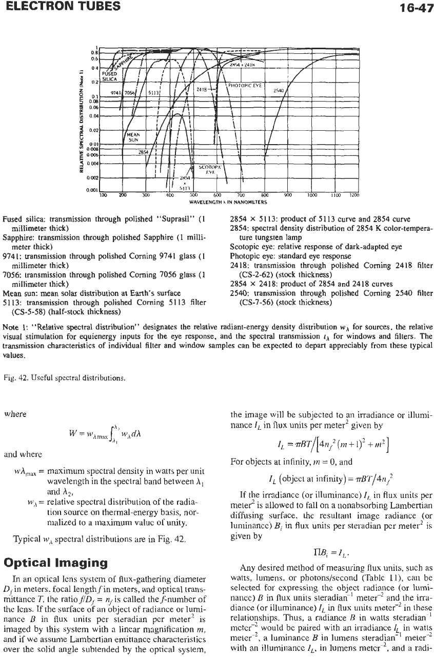
16-47
Fused silica: transmission through polished “Suprasil”
(1
Sapphire: transmission through polished Sapphire
(1
milli-
9741: transmission through polished Coming 9741 glass
(1
7056: transmission through polished Coming 7056 glass (1
Mean sun: mean solar distribution at Earth’s surface
51 13: transmission through polished Coming 5113 filter
millimeter thick)
meter thick)
millimeter thick)
millimeter thick)
(CS-5-58) (half-stock thickness)
2854
X
5113: product of 5113 curve and 2854 curve
2854: spectral density distribution of 2854
K
color-tempera-
Scotopic eye: relative response
of
dark-adapted eye
Photopic eye: standard eye response
2418: transmission through polished Coming 2418 filter
2854
X
2418: product
of
2854 and 2418 curves
2540: transmission through polished Coming 2540 filter
ture tungsten lamp
(CS-2-62) (stock thickness)
(CS-7-56) (stock thickness)
Note
1:
“Relative spectral distribution” designates the relative radiant-energy density distribution
wA
for
sources, the relative
visual stimulation for equienergy inputs for the eye response, and the spectral transmission
tA
for windows and filters. The
transmission characteristics
of
individual filter and window samples can be expected to depart appreciably from these typical
values.
Fig. 42.
Useful
spectral
distributions.
where
and where
wAmax
=
maximum spectral density
in
watts per unit
wavelength in the spectral band between
A,
and
A,,
w,,
=
relative spectral distribution of the radia-
tion source on thermal-energy basis,
nor-
malized to a maximum value of unity.
Typical
w,,
spectral distributions are in Fig.
42.
Optical Imaging
In
an
optical lens system of flux-gathering diameter
Df
in meters, focal lengthfin meters, and optical trans-
mittance
T,
the ratiofiDS
=
nf
is called thef-number of
the lens.
If
the surface of an object
of
radiance or lumi-
nance
B
in flux units per steradian per meter’ is
imaged by this system with a linear magnification
rn,
and if we assume Lambertian emittance characteristics
over the solid angle subtended by the optical system,
the image will be subjected to an irradiance or illumi-
nance
ZL
in
flux units per meter2 given by
IL
=
.rrB7/[4nf?
(rn
+
1)’
+
m’]
For
objects at infinity,
rn
=
0,
and
ZL
(object at infinity)
=
?rBT/4nf2
If the irradiance (or illuminance)
I,
in
flux
units per
mete? is allowed to fall
on
a
nonabsorbing Lambertian
diffusing surface, the resultant image radiance (or
luminance)
B,
in flux units per steradian per meter2 is
given by
m,
=zL.
Any desired method of measuring flux units, such as
watts. lumens, or photons/second (Table
ll),
can be
selected for expressing the object radiance
(or
lumi-
nance)
B
in
flux
units steradian-’ meter-’ and the irra-
diance (or illuminance)
Z,
in
flux
units meter-’ in these
relationships. Thus,
a
radiance
B
in watts steradian-’
meter-’ would be paired with
an
irradiance
Z,
in watts
meter-’,
a
luminance
B
in lumens steradian-‘ meter-2
with
an
illuminance
IL,
in lumens meter-‘, and a radi-
16-48
REFERENCE
DATA
FOR
ENGINEERS
ance
B
in photons second-’ steradian-’ meter-’ with an
irradiance
Z,
in photons second-’ meteF2.
Any spectral distribution modifications, if present,
would be included in the numerical magnitude of the
lens transmission
T,
defined as the ratio of the total
output flux from the optical system to the correspond-
ing input flux.
Selection of appropriate alternative pairs of lumi-
nance and illuminance units when the flux units
are
not
explicitly stated (first column of Table 11) must be
made with care. Thus candle centimeter-’ (or stilb)
would be paired with hot, candle meter-’ (or nit) with
lux, and candle foot with footcandle. Even greater
difficulty arises when the factor
Il
in the preceding
relationships is absorbed or included in the units of
luminance. Thus the product
Ill?
in
apostilbs would be
paired with
Z,
in lux, the product
ID
in lamberts with
I,
in phots, the products
Ill?
in millilamberts with
I,
in
milliphots, and the product
rIB
in footlamberts with
ZL
in footcandles. These difficulties are avoided by the
use of the compatible systems of radiation units shown
in Table
10.
4
Typical Approximate
Illumination Values at the
Surface
of
the Earth
Sun at zenith
-
lo4
footcandles
=
io5
lumens meter-’
-
3
x
IO-’
lumens meter-2
Full moon
-
3
x
lo-’
footcandles
Typical Approximate
Bright ness
Va
I
u
es
Highlights, 35-milli-
meter movie
Page brightness for
reading fine print
November football
field
Surface of
moon
seen from Earth
Summer baseball
field
Surface of 40-watt
frosted lamp bulb
Crater
of
carbon arc
Sun
seen
from
Earth
footlamberts
-4
=
10
-
50
-
1.5
x
io3
=
3
x
io3
-
8
x
io3
=
4.5
x
io7
=
5.2
x
lo8
1m sr-’ m-’
=
100
-
3
x
lo2
=
1.5 x10³
-5~10~
=
io5
=
io9
-
2.5
x
10’
=
1.5
x
10“
LIGHT-SENSING TUBES
ImageTubes and Image
Intensifiers
An image tube* is an optical-image-in to optical-
image-out electron-tube device, combining
an
input
photocathode and an output phosphor screen such that
photoelectrons emitted from each point
on
the photo-
cathode subsequently excite a corresponding individ-
ual
image “point” on the phosphor screen.
Various
focusing means, including magnetic and electrostatic
electron lenses, may be used to assure maximum
point-to-point correlation between the input and output
images. The principal operating requirements are
a
lens to form the input image and
a
high-voltage supply,
typically 5-25 kilovolts, to provide sufficient electron-
beam energy to excite the output phosphor screen.
If
means are provided within the image tube to
amplify the photoelectrons before they strike the out-
put phosphor screen, or if the tube without such means
produces
a
much brighter output image than the input
image would produce
on
a
diffusing screen, the tube is
commonly called an image-intensifier tube.
Image-intensifier tubes are used to amplify the
brightness of
a
faint input image for better visual or
photographic viewing, whereas image tubes without
amplification are used to convert radiation from one
spectral region to another (image conversion) or to
perform such control operations
as
optical shuttering
by programming the applied high voltage.
The total output flux
dW,,
in
watts exiting (through
2H steradians) from the phosphor-screen faceplate of
an image-intensifier tube for an input monochromatic
flux
dW,,
in
watts at
a
wavelength
A
is given by
dW,
=s,,GCeW(V-&)dW,,
=
G,,dW,,
where
G,,
=
monochromatic wattage gain
of
the image-
intensifier tube at
a
wavelength A-ratio of the
total output flux
dWo
in watts to the input
monochromatic flux
dW,,
in watts
s,,
=
radiant sensitivity of the input photocathode
in
amperes per watt (see Fig. 13, Chapter 21)
G
=
internal current gain ratio of the image-intensi-
fier tube
=
ratio of the current bombarding the
output phosphor screen to the corresponding
photocurrent leaving the input photocathode
total radiated flux in watts to the exciting elec-
tron-beam power in watts dissipated
in
the
particles of the output phosphor screen
V
=
energy of the electron beam in volts bombard-
ing the output phosphor screen
V,
=
extrapolated knee voltage
of
the output phos-
phor screen.
If the phosphor screen radiates flux according to
Lambert’s law (usually only approximately valid), the
CeW
=
absolute phosphor efficiency
=
ratio of the
*
Photo-Electrical Image Devices,
Advances in Electron-
ics and Electron Physics, Vols. 12, 16, 22A, and 22B
(New
York
and
London: Academic
Press,
1960, 1962, and 1966),
H.
V. Soule,
Electro-Optical Photography at
Low
Illumina-
tion Levels
(New
York:
John
Wiley
&
Sons,
1968).
ELECTRON TUBES
16-49
corresponding output image radiance
R,,
in watts
steradian-' meter? is given by
R,
=
G,,
I,,
lIIm2
where
IA,
=
input image irradiance on the photocathode
expressed in watts meter-' at the wavelength
m
=
differential magnification ratio
of
the image
41
tube
=
output incremental image size divided
by the corresponding input incremental image
size.
For
a
spectrally distributed input flux having
a
known relative spectral distribution
wA
and
a
known
total radiated power
W,,,,,
in watts between the wave-
length limits
A,
and
A,,
the resulting total output flux
W,,
in watts exiting from the image tube,
is
given by
x
Gg
w(~-~)~Ai,2
=
GA~~\ZWAIAZ
where
sAmak
=
peak radiant sensitivity of the input photo-
cathode in amperes per watt
n,
=
relative radiant sensitivity of the input
photocathode
as
a
function of wavelength
A
normalized to unity maximum
wA
=
relative spectral distribution of the power
density spectrum of the input flux normal-
ized to unity maximum
G,,
h2
=
wattage gain of the image tube for the rela-
tive spectral distribution
w,,
and the wave-
length limits
A,
and
A,.
Typical values for the magnitude of the dimension-
less
spectral-matching-factor ratio
are
given by
The total output flux
L,,
in lumens exiting from an
image tube, corresponding to the total output flux
W,
in watts, can be computed from the flux conversion
relationships given in the section on radiometry and
photometry, or from the following relationship
=
GLLi
where
GL
=
luminous gain of the image intensifier tube
=
ratio of the output flux in lumens to the cor-
responding input flux in lumens for the spec-
tral input distribution w,
E,
=
standard tabulated average relative photopic
eye response
w,,,
=
relative spectral density distribution
of
the
output flux
Li
=
input flux in lumens
The typical values of the dimensionless spectral
matching factors can be used to determine the magni-
tude of the dimensionless integral ratios appearing in
these relationships. For the special case where the
input flux
L,
(2854)
in lumens is generated by
a
2854
K
color-temperature tungsten-filament lamp, the output
flux
L,(2854)
in lumens is given by
L,
(2854)
=
S(2854)Gg
~
x
(V-Vk)L,(2854)
=
GL (2854)L, (2854)
where
GL(2854j
=
luminous gain
of
the image intensifier
for
2854
K
tungsten-lamp radiation
S(2854)
=
luminous sensitivity of the input photo-
cathode for
2854 K
tungsten-lamp radi-
ation
The magnitude of the luminous gain
GL(2854j
is com-
monly used to characterize the image intensification
properties of an image-intensifier tube.
If the output phosphor screen radiates flux accord-
ing to Lambert's law (usually only approximately
valid), the output image luminance (or brightness)
B,
in lumens steradian-' meter-' is given by
B,
=
G,I,
/m2
where
GL
=
I,
=
rn=
luminous gain of the image intensifier for
input spectral distribution w,,
input illuminance (or illumination) on the
photocathode in lumens meter-' for the spec-
tral distribution w,
differential magnification ratio of the image
tube
=
output incremental image size divided
by the corresponding input incremental image
size
Internal current gain
G
of an image-intensifier tube
can be obtained by the use
of
an internal sandwich elec-
trode,
in
which an auxiliary or sandwich photocathode
is mounted
in
close proximity to and following an auxil-
iary or sandwich phosphor. Photoelectrons from the
input photocathode
of
the tube
are
then imaged onto this
sandwich phosphor screen, and the flux from this screen
is coupled to the sandwich photocathode, generating an
enhanced photocurrent. The current gain ratio
G
of this
sandwich phosphor-photocathode combination, defined
16-50
REFERENCE
DATA
FOR ENGINEERS
as the ratio of
output
photocurrent to input photocurrent,
is given by
where
s,,
max,
sand
=
peak monochromatic responsivity of
the sandwich photocathode in amperes
watt-’
wA
(sand)
=
relative spectral distribution of the flux
emitted by the sandwich phosphor
screen
sandwich photocathode
phosphor screen
in
watts watt-’
barding the sandwich phosphor screen
the sandwich phosphor screen
y
=
optical coupling efficiency of the sand-
wich electrode
=
ratio
of
the flux fall-
ing onto the sandwich photocathode
to
the corresponding flux emitted by the
sandwich phosphor screen
The combination of a phosphor screen and a photo-
cathode
to
produce current gain
G
can
also
be achieved
by optically coupling the output flux from one image
tube to the input of a second tube.
Resolution in image tubes and image-intensifier
tubes is a subjective parameter describing the number
of pairs
of
equally spaced illuminated and unillumi-
nated bars per unit distance at the photocathode
imaged onto the input photocathode surface that can
just be distinguished visually by a trained observer
under stated test conditions.
F,,
(sand)
=
the relative spectral distribution of the
Zw.
sand
=
absolute efficiency
of
the sandwich
Vsmd
=
electron beam energy in volts bom-
Vk,
sand
=
extrapolated knee voltage in volts for
TRANSLUCENT
PHOTOCATHODE
COLLECTOR
-
MESH
Distortion
is
a
parameter describing any change in
the geometric shape
of
the output image compared with
the input image. Radially increasing magnification
leads
to
“pincushion” distortion; radially decreasing
magnification leads
to
“barrel” distortion; and radially
changing image rotation leads
to
“S’
distortion.
Gas
Photodiodes
In
diode phototubes not containing a high vacuum,
ionization by collision of electrons with neutral mole-
cules may occur
so
that more than one electron reaches
the anode for each originally emitted photoelectron.
This “gas amplification factor” has a value of between
3
and
5;
a
higher factor causes instabilities. Gas-tube
operation is restricted to frequencies below about
10
000
hertz.
Image
Orthicons
The image orthicon* is a camera tube that is widely
used for commercial television. This fact derives from
its high sensitivity, its close spectral-sensitivity match
to the human eye, and its relatively fast response.
Good quality commercial television pictures can be
generated by an image orthicon viewing a
5-to-20-
footlambert
(-
15-50 lumen steradian-’ meter-2) scene
through an f/5.6 lens. The image orthicon is generally
available with either
S-10
or
S-20
spectral response
(see Fig.
13,
Chapter
21)
and is capable of
500
picture
elements per raster height
(9.9
line pairs/millimeter) at
30%
video-amplitude response.
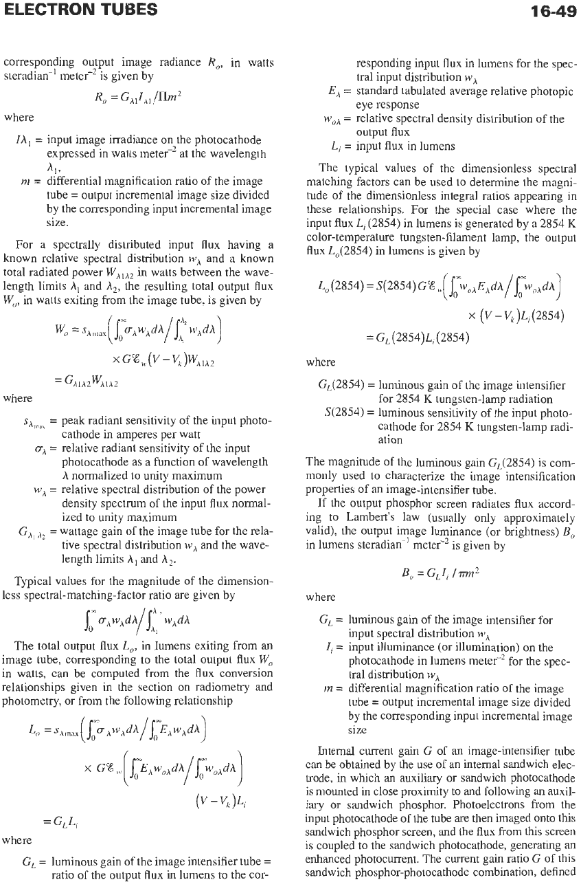
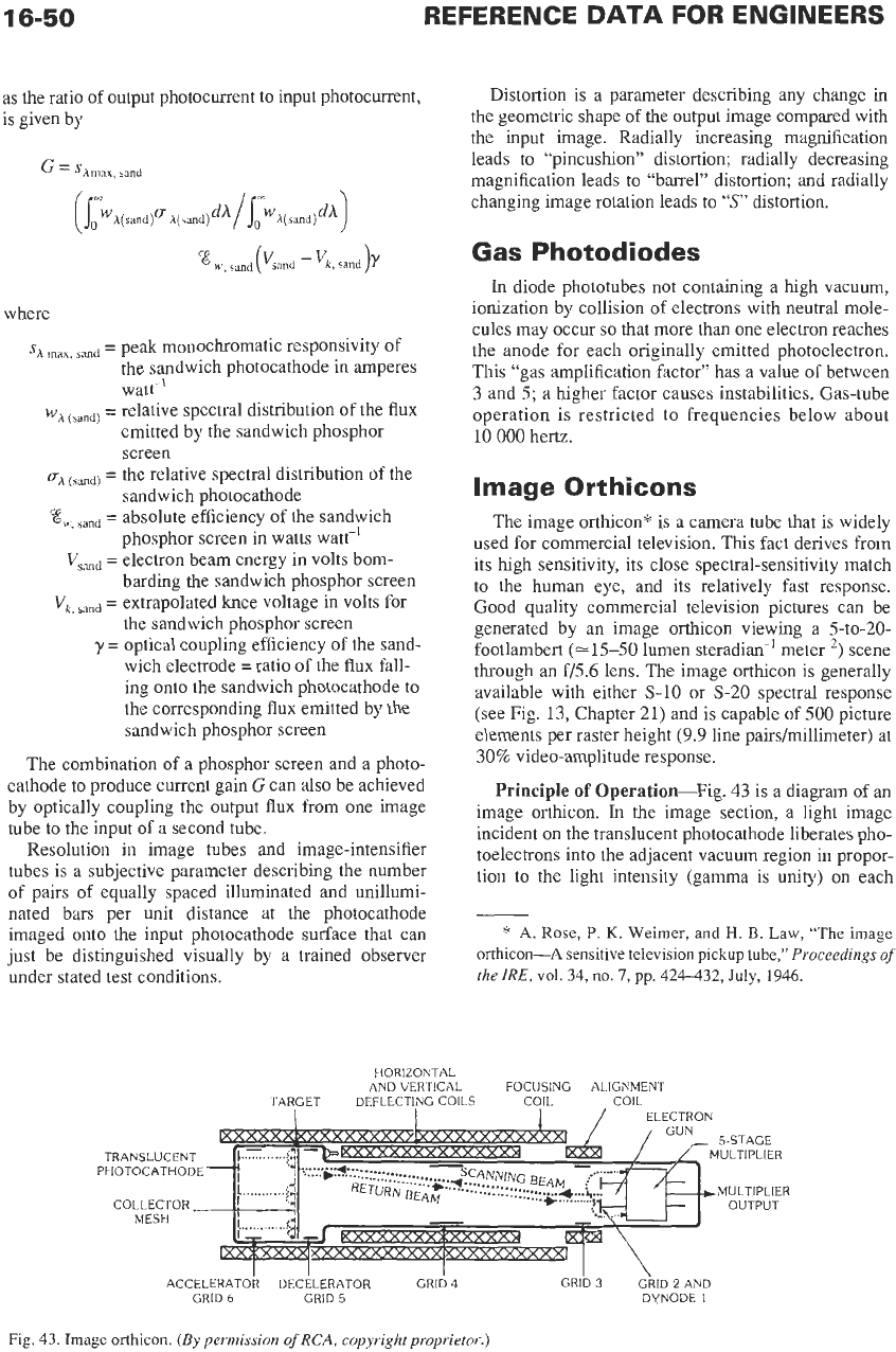
Principle
of
Operation-Fig.
43
is a diagram of an
image orthicon.
In
the image section, a light image
incident on the translucent photocathode liberates pho-
toelectrons into the adjacent vacuum region in propor-
tion to the light intensity (gamma is unity)
on
each
*
A.
Rose,
P.
K.
Weimer, and
H.
B.
Law, “The image
orthicon-A
sensitive television pickup
tube,”
Proceedings
of
the
IRE,
vol. 34, no.
7,
pp.
424-432,
July,
1946.
HORIZONTAL
AND VERTICAL FOCUSING ALIGNMENT
TARGET DEFLECTING COILS COIL COIL
I
I
I
/
ELECTRON
._
...*
Ii
.............
dl
,
-
\
\,
ACCELERATOR DECELERATOR GRID
4
GRID
3
GklD
2
AND
GRID
6
GRID
5
DYNODE
1
Fig. 43. Image orthicon.
(By permission
of
RCA,
copyright proprietor.)
16-51
element of the cathode. These photoelectrons are
accelerated toward and magnetically focused onto the
surface of a thin semiconducting target. Electrons
strike this target with sufficient energy to liberate a
larger number of secondary electrons (typically five)
for each incident primary. The secondary electrons are
collected by a mesh closely spaced from the target
membrane. Hence, by depletion of electrons from the
thin membrane, incremental areas become positive in
proportion to the number of photoelectrons sh-iking
each element.
In
cases of high-light-level operation,
parts of the target may become charged to target (col-
lector) mesh potential, and saturation charge results.
This phenomenon accounts for the so-called “knee” in
the signal-versus-illumination transfer curve (Fig. 43).
Because the target membrane is very thin, of the
order of microns, a charge distribution pattern formed
on the image-section surface appears nearly simulta-
neously and identically
on
the
scanning-section surface.
In
the scanning section, an electron gun generates a
highly apertured electron beam from a fraction to tens
of microamperes in intensity.
A
solenoidal magnetic-
focus coil and saddle-type deflection coils surrounding
the scan section focus this beam on the insulator target
and move it across the target. Scan-beam electrons
impinge on the target at very low velocity, giving rise
to relatively few secondary electrons. The target acts
somewhat as a retarding-field electrode and reflects a
large number of the beam electrons that have less than
average axial velocity. These two phenomena-small
but finite secondary emission and reflection
of
slow
beam electrons-limit scan-beam modulation
to
a
maximum of about 30% at high light levels, and to 2
orders less at threshold. As will be shown later, the
large unmodulated return beam current is the primary
source of noise in the image orthicon.
Another problem created by the retarding-field
aspect of low-velocity target scanning appears when
the deflected beam does not strike the target normally.
Since the entire beam-velocity component normal to
the surface is now reduced by
the
cosine of the angle
of incidence, the effective beam impedance is greatly
increased. To overcome this problem, the decelerating
field between grids 4 and
5
is shaped such that the
electron beam always approaches normal to the plane
of the target at a low velocity. If the elemental area on
the target is positive, then electrons from the scanning
beam deposit until the charge is neutralized. If the ele-
mental area is at cathode potential (corresponding
to
a
dark picture area), no electrons are deposited.
In
both
cases, the excess beam electrons are turned back and
focused into a five-stage electron multiplier. The
charges existing on either side of the semiconductive
target membrane will, by conductivity, neutralize each
other in less than one frame time. Electrons turned
back at the target form a return beam that has been
amplitude-modulated
in
accordance with the charge
pattern of the target.
The return beam is redirected by the deflection and
focus fields toward the electron gun where it origi-
nated. Atop the electron gun, and forming the final
aperture for that gun, is a flat secondary-emitting sur-
face comprising the first dynode of the electron multi-
plier. The return beam strikes this surface, generating
secondary electrons in a ratio of approximately 4:
1.
Grid 3 facilitates a more complete collection by
dynode
2
of the secondary electrons emitted from dyn-
ode
1.
The gain of the multiplier is high enough that in
operation the limiting noise is the shot noise of the
returned electron beam rather than the input noise of
the video amplifier.
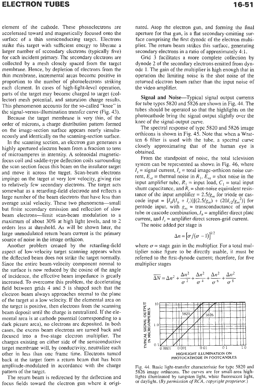
Signal
and
Noise-Typical signal output currents
for tube types 5820 and 5826
are
shown in Fig. 44. The
tubes should be operated
so
that the highlights on the
photocathode bring the signal output slightly over
the
knee of the signal-output curve.
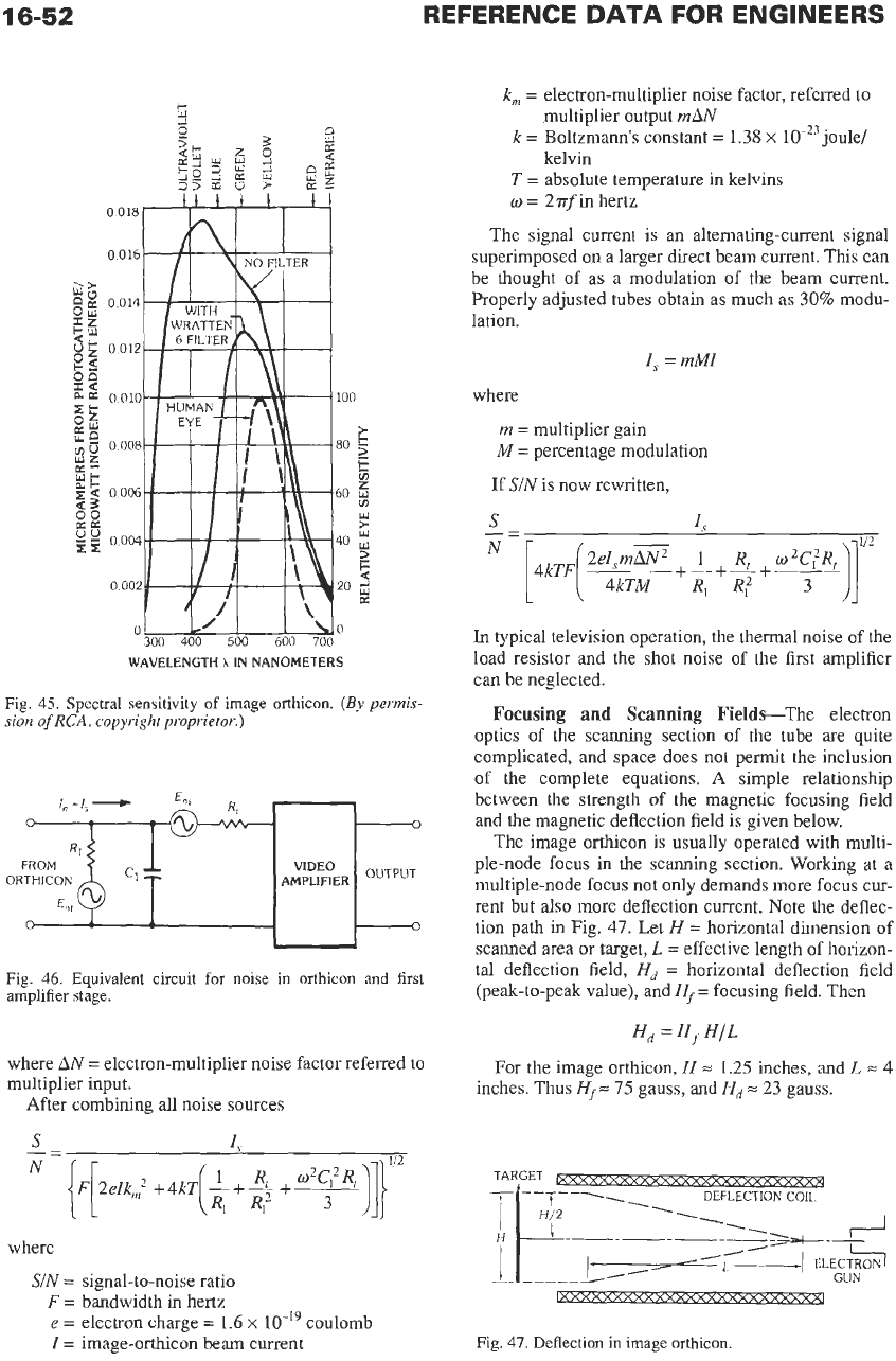
The spectral response of type 5820 and 5826 image
orthicons is shown in Fig. 45. Note that when a Wrat-
ten
6
filter is used with the tube, a spectral curve
closely approximating that of the human eye is
obtained.
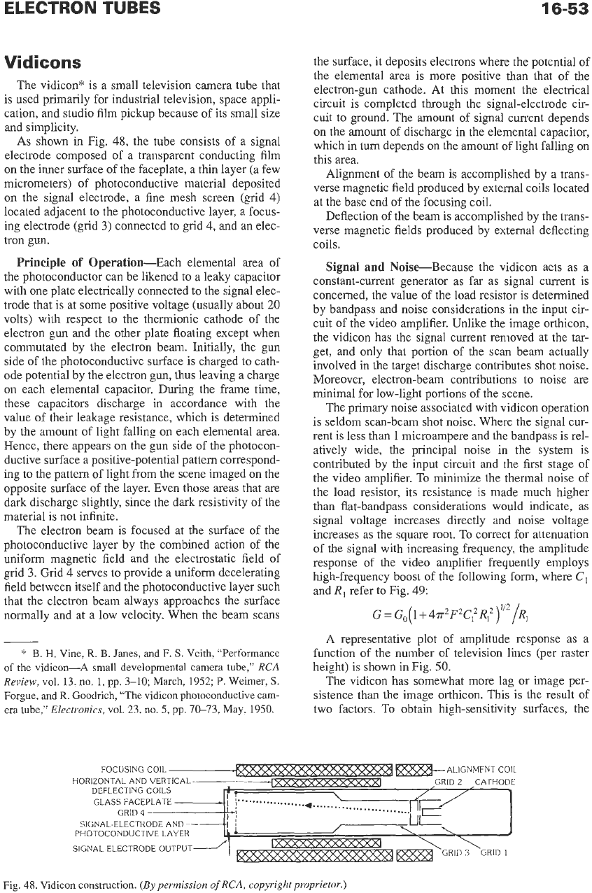
From the standpoint of noise, the total television
system can be represented as shown in Fig.
46,
where
Z,
=
signal current,
Z,
=
total image-orthicon noise cur-
rent,
E,,
=
thermal noise in
R,, E,,
=
shot noise in the
input amplifier tube,
R,
=
input load,
C,
=
total input
shunt capacitance, and
R,
=
shot-noise equivalent resis-
tance of the input amplifier
=
2.5/g,,1 for triode or cas-
code input
=
[Ib/(Zb
+
Zc)][(2.5/gnl)
+
(20Ic2/g,2)] for
pentode input, with g,
=
transconductance of input
tube or cascode combination,
Zb
=
amplifier direct plate
current, and
I,
=
amplifier direct screen-grid current.
The noise added per stage is
An
=
[(T/((T
-
l)]”’
where
(T
=
stage gain in
the
multiplier. For a total mul-
tiplier noise figure to be directly usable, it must be
referred to the first-dynode current; therefore, for five
multiplier stages
-
An2 An2 An2 An2
Ah’
=
An2
+-+-+-
+-
u2
u4
u6 u8
5
10
2:
a::
$!2
gg
<?
sc
5:
0
1
z*
10
VIIWI
Ill1
I
/Ill
I
Ill
00001
0001
0
01
01
10
HIGHLIGHT ILLUMINATION ON
PHOTOCATHODE IN FOOTCANDLES
Fig.
44.
Basic light-transfer characteristic for
type
5820
and
5826
image orthicons. The curves
are
for
small-area high-
lights illuminated
by
tungsten light, white fluorescent light,
or daylight.
(By
permission
of
RCA,
copyright proprietor.)
16-52
REFERENCE
DATA
FOR ENGINEERS
WAVELENGTH
A
IN
NANOMETERS
Fig.
45.
Spectral sensitivity
of
image orthicon.
(By
permis-
sion
of
RCA,
copyright proprietor.)
FROM
ORTHICON
E",
Fig.
46.
Equivalent circuit for
noise
in
orthicon
and
first
amplifier stage.
where
U
=
electron-multiplier noise factor referred to
multiplier input.
After combining all noise sources
where
SIN
=
signal-to-noise ratio
F
=
bandwidth in hertz
e
=
electron charge
=
1.6
x
I
=
image-orthicon beam current
coulomb
k,
=
electron-multiplier noise factor, referred
to
joule/
multiplier output
mAN
k
=
Boltzmann's constant
=
1.38
x
kelvin
T
=
absolute temperature in kelvins
o
=
2rrf
in
hertz
The signal current is an alternating-current signal
superimposed on a larger direct beam current. This can
be thought of as a modulation
of
the beam current.
Properly adjusted tubes obtain as much as
30%
modu-
lation.
I,
=mMI
where
rn
=
multiplier gain
M
=
percentage modulation
If
SIN
is now rewritten,
S
I,
In
typical television operation, the thermal noise of the
load resistor and the shot noise of the first amplifier
can be neglected.
Focusing and Scanning
Fields-The electron
optics of the scanning section
of
the tube are quite
complicated, and space does not permit the inclusion
of the complete equations. A simple relationship
between the strength
of
the magnetic focusing field
and
the
magnetic deflection field is given below.
The image orthicon
is
usually operated with multi-
ple-node focus in
the
scanning section. Working
at
a
multiple-node focus not only demands more focus cur-
rent but
also
more deflection current. Note the deflec-
tion path in Fig.
47.
Let
H
=
horizontal dimension of
scanned area or target,
L
=
effective length of horizon-
tal deflection field,
Hd
=
horizontal deflection field
(peak-to-peak value), and
Hf=
focusing field. Then
H,
=
H,.
HfL
For
the image orthicon,
H
=
1.25
inches,
and
L
)=
4
inches. Thus
Hf
=
75
gauss, and
Hd
=
23 gauss.
TARGET
DEFLECTION
COIL
-.
.
Fig.
47.
Deflection
in
image orthicon.
16-53
Vidicons
The vidicon* is a small television camera tube that
is used primarily for industrial television, space appli-
cation, and studio film pickup because of its small size
and simplicity.
As shown
in
Fig.
48,
the tube consists of a signal
electrode composed of a transparent conducting film
on
the inner surface of the faceplate, a thin layer (a few
micrometers) of photoconductive material deposited
on
the signal electrode, a fine mesh screen (grid
4)
located adjacent to the photoconductive layer, a focus-
ing electrode (grid
3)
connected to grid
4,
and an elec-
tron gun.
Principle
of
Operation-Each elemental area of
the photoconductor can be likened to a leaky capacitor
with one plate electrically connected to the signal elec-
trode that is at some positive voltage (usually about
20
volts) with respect to the thermionic cathode of the
electron gun and the other plate floating except when
commutated by the electron beam. Initially, the gun
side
of
the photoconductive surface is charged to cath-
ode potential by the electron
gun,
thus leaving a charge
on each elemental capacitor. During the frame time,
these capacitors discharge in accordance with the
value of their leakage resistance, which
is
determined
by the amount of light falling
on
each elemental area.
Hence, there appears
on
the gun side of the photocon-
ductive surface a positive-potential pattern correspond-
ing to the pattern of light from the scene imaged
on
the
opposite surface of the layer. Even those areas that are
dark discharge slightly, since the dark resistivity of the
material is not infinite.
The electron beam is focused at the surface of the
photoconductive layer by the combined action of the
uniform magnetic field and the electrostatic field
of
grid
3.
Grid
4
serves to provide a uniform decelerating
field between itself and the photoconductive layer such
that the electron beam always approaches the surface
normally and at a low velocity. When the beam scans
*
B.
H.
Vine,
R. E.
Janes, and
F. S.
Veith, “Performance
of the vidicon-A small developmental camera tube,”
RCA
Review,
vol. 13, no.
1,
pp. 3-10; March, 1952;
P.
Weimer,
S.
Forgue, and
R.
Goodrich,
“The
vidicon photoconductive cam-
era tube.”
Electronics,
vol. 23, no. 5, pp. 70-73, May, 1950.
the surface, it deposits electrons where the potential of
the elemental area is more positive than that of the
electron-gun cathode. At
this
moment the electrical
circuit is completed through the signal-electrode cir-
cuit to ground. The amount of signal current depends
on the amount of discharge in the elemental capacitor,
which in
turn
depends on the amount of light falling
on
this area.
Alignment of the beam
is
accomplished by a trans-
verse magnetic field produced by external coils located
at the base end
of
the focusing coil.
Deflection of the beam is accomplished by the trans-
verse magnetic fields produced by external deflecting
coils.
Signal and Noise-Because the vidicon acts as a
constant-current generator as far as signal current is
concerned, the value of the load resistor is determined
by bandpass and noise considerations
in
the input cir-
cuit of the video amplifier. Unlike the image orthicon,
the vidicon has the signal current removed at the tar-
get, and only that portion of the scan beam actually
involved in the target discharge contributes shot noise.
Moreover, electron-beam contributions to noise are
minimal for low-light portions of the scene.
The primary noise associated with vidicon operation
is seldom scan-beam shot noise. Where the signal cur-
rent is less than
l
microampere and the bandpass is rel-
atively wide, the principal noise
in
the system is
contributed by the input circuit and the first stage of
the video amplifier.
To
minimize the thermal noise of
the load resistor, its resistance is made much higher
than flat-bandpass considerations would indicate, as
signal voltage increases directly and noise voltage
increases as the square root. To correct for attenuation
of the signal with increasing frequency, the amplitude
response of the video amplifier frequently employs
high-frequency boost of the following form, where
C,
and
R,
refer to Fig.
49:
G
=
Go
(1
+
4,rr2F2C:
R:
)”’
/Rl
A representative plot of amplitude response as a
function
of
the number of television lines (per raster
height) is shown
in
Fig.
50.
The vidicon has somewhat more lag or image per-
sistence than the image orthicon. This is the result of
two factors.
To
obtain high-sensitivity surfaces, the
FOCUSING COIL
-ALIGNMENT
COIL
HORIZONTAL AND VER GRID
2
CATHODE
DEFLECTING COILS
GLASS FACEPLATE
GRID
4
SIGNAL-ELECTR
PHOTOCONDUCT
SIGNAL-ELECTRO
Fig.
48.
Vidicon construction.
(By
permission
of
RCA,
copyright proprietor.)
16-54
REFERENCE
DATA
FOR ENGINEERS
Fig.
49.
Equivalent input circuit
for
first-stage amplifier in
vidicon circuit.
NUMBER
OF
TELEVISION LINES
Fig.
50.
Vidicon resolution, showing uncompensated and
compensated horizontal responses. Highlight signal-electrode
microamperes
=
0.35; test
pattern
=
transparent square-wave
resolution wedge;
80
television lines
=
1-megahertz band-
width.
(By
permission
of
RCA, copyright proprietor.)
photoconductive decay time is made as long as tolera-
ble, because quantum efficiency is limited by the ratio
of effective carrier lifetime to carrier transit time
across the photoconductor. A second source of lag is
simply the
RC
time constant of
the
target recharging
circuit, that is, the target capacitance and the beam
impedance.
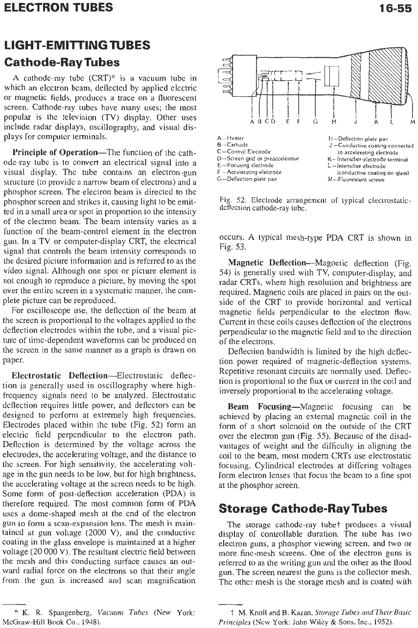
The spectral response of most commercial vidicons
designated
S-18
is more actinic than that
of
the human
eye. Fig.
51
compares these responses with the spec-
trum
of
a 2854
K
tungsten source.
Variations
of
the
Vidicon
Interest in optical guidance and surveillance from
aircraft and spacecraft has given rise to a wide variety
WAVELENGTH IN ANGSTROM UNITS
Fig.
5
1.
Spectral response
of
vidicon.
(By
permission
of
RCA,
copyright proprietor,)
of
vidicon camera tubes.
To
treat these variations in
detail becomes encyclopedic, but the following gives
some indication
of
the choices now available to the
user.
Effective Sensitivity-True photoconductive tubes
now offer sensitivities of 150-200 nanoamperes for
1/2-footcandle illumination with
20
nanoamperes dark
current. Improved methods
of
deposition
of
photocon-
ductors have made possible higher-voltage operation
without objectionable dark shading. Special devices
using junction effects promise even better sensitivity.
Spectral Response-Available photoconductors,
taken
as
a whole, provide sensitivity over the entire
visible range with usual
(7056)
glass windows.
Quartz-window tubes offer useful sensitivity to below
2000
angstroms. Numerous applications of direct exci-
tation
of
photoconductors by X-radiation have been
reported. High-velocity electron excitation (bombard-
ment-induced conductivity) is
also
in
use.
Size and Deflection-Vidicons are available
in
sizes ranging from
1/2
inch to
2
inches in diameter.
Various
combinations of deflection and focus
are
avail-
able.
Storage-A number of manufacturers have pro-
duced vidicons with long-storage characteristics.
Many are merely long-lag tubes; however, a few rely
on high-resistivity materials
or
on barrier layers to
retain stored charge through minimal dark current.
One such device, once exposed properly to a scene,
regenerates the scene through readout over a period of
the order of half an hour.
ELECTRON TUBES
16-55
LIGHT-EMITTING TUBES
Cathode-Ray Tubes
A cathode-ray tube (CRT)* is
a
vacuum tube in
which an electron beam, deflected by applied electric
or magnetic fields, produces
a
trace on
a
fluorescent
screen. Cathode-ray tubes have many uses; the most
popular is the television (TV) display. Other uses
include radar displays, oscillography, and visual dis-
plays for computer terminals.
Principle
of
Operation-The function of the cath-
ode-ray tube is
to
convert an electrical signal into
a
visual display. The tube contains an electron-gun
structure (to provide
a
narrow beam of electrons) and
a
phosphor screen. The electron beam is directed to the
phosphor screen and strikes it, causing light to be emit-
ted in
a
small area or spot in proportion to the intensity
of the electron beam. The beam intensity varies
as
a
function of the beam-control element in the electron
gun. In a TV or computer-display CRT, the electrical
signal that controls the beam intensity corresponds
to
the desired picture information and is referred to as the
video signal. Although one spot or picture element is
not enough
to
reproduce
a
picture, by moving the spot
over the entire screen in
a
systematic manner, the com-
plete picture can be reproduced.
For oscilloscope use, the deflection of the beam at
the screen is proportional to the voltages applied to the
deflection electrodes within the tube, and a visual pic-
ture of time-dependent waveforms can be produced on
the screen in the same manner as
a
graph is drawn on
paper.
Electrostatic Deflection-Electrostatic deflec-
tion is generally used in oscillography where high-
frequency signals need to be analyzed. Electrostatic
deflection requires little power, and deflectors can be
designed to perform at extremely high frequencies.
Electrodes placed within the tube (Fig. 52) form an
electric field perpendicular to the electron path.
Deflection is determined by the voltage across the
electrodes, the accelerating voltage, and the distance to
the screen. For high sensitivity, the accelerating volt-
age in the gun needs to be low, but for high brightness,
the accelerating voltage at the screen needs to be high.
Some form of post-deflection acceleration (PDA) is
therefore required. The most common form of PDA
uses
a
dome-shaped mesh at the end of the electron
gun
to
form
a
scan-expansion lens. The mesh
is
main-
tained at gun voltage (2000 V), and the conductive
coating
in
the glass envelope is maintained at
a
higher
voltage (20
000
V). The resultant electric field between
the mesh and this conducting surface causes an out-
ward radial force on the electrons
so
that their angle
from the gun is increased and scan magnification
*
K.
R.
Spangenberg,
Vacuum Tubes
(New
York:
McGraw-Hill
Book
Co.,
1948).
A-Heater H-Deflection-plate pair
B-Cathode
C-Control Electrode to accelerating electrode
D-Screen grid
or
preaccelerator
E
-Focusing
electrode L-Intensifier electrode
F
-Accelerating electrode
G-Deflection-plate pair M-Fluorescent screen
J
-Conductive coating connected
K-Intensifier-electrode terminal
(conductive coating on glass)
Fig. 52. Electrode arrangement
of
typical electrostatic-
deflection cathode-ray tube.
occurs. A typical mesh-type PDA CRT is shown in
Fig.
53.
Magnetic Deflection-Magnetic deflection (Fig.
54)
is generally used with TV, computer-display, and
radar CRTs, where high resolution and brightness are
required. Magnetic coils are placed in pairs on the out-
side of the CRT
to
provide horizontal and vertical
magnetic fields perpendicular to
the
electron flow.
Current in these coils causes deflection of the electrons
perpendicular to the magnetic field and to the direction
of the electrons.
Deflection bandwidth is limited by the high deflec-
tion power required of magnetic-deflection systems.
Repetitive resonant circuits are normally used. Deflec-
tion is proportional to the flux or current in the coil and
inversely proportional to the accelerating voltage.
Beam Focusing-Magnetic focusing can be
achieved by placing an external magnetic coil in the
form of
a
short solenoid on the outside of the CRT
over the electron gun (Fig. 55). Because of the disad-
vantages of weight and the difficulty in aligning the
coil
to
the beam, most modem CRTs use electrostatic
focusing. Cylindrical electrodes at differing voltages
form electron lenses that focus the beam to
a
fine spot
at
the phosphor screen.
Storage Cathode-Ray Tubes
The storage cathode-ray tube? produces
a
visual
display of controllable duration. The tube
has
two
electron guns,
a
phosphor viewing screen, and two or
more fine-mesh screens. One of the electron guns is
referred to
as
the writing gun and the other
as
the flood
gun. The screen nearest the guns is the collector mesh.
The other mesh is the storage mesh and is coated with
t.
M.
Knoll
aqd
E.
Kazan,
Storage Tubes and Their
Basic
Principles
(New
York
John
Wiley
&
Sons, Inc.,
1952).