Middleton W.M. (ed.) Reference Data for Engineers: Radio, Electronics, Computer and Communications
Подождите немного. Документ загружается.

16-56
REFERENCE
DATA
FOR
ENGINEERS
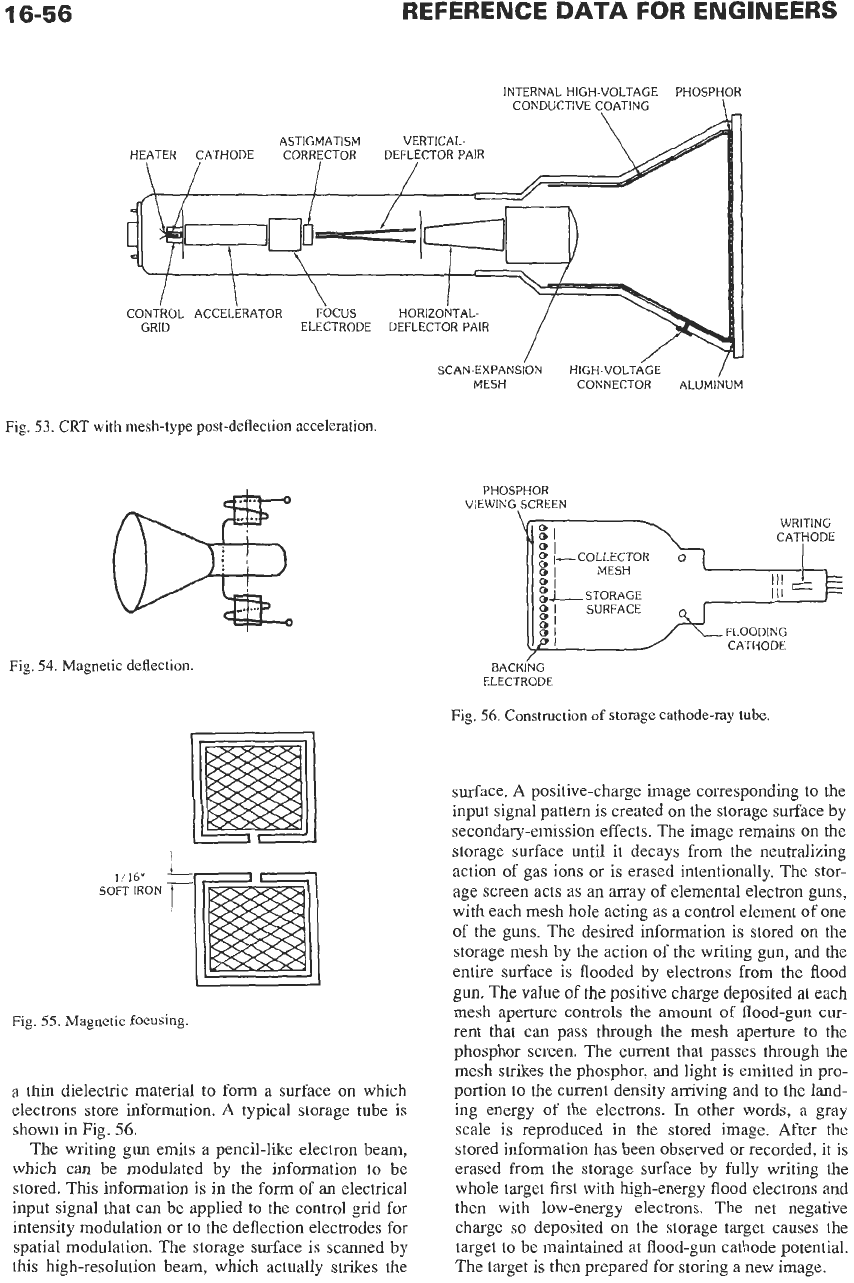
INTERNAL HIGH-VOLTAGE PHOSPHOR
ATISM VERTICAL-
CTOR DEFLECTOR PAIR
GRID
SCAN-EXPANS
MESH CONNECTOR ALUMINUM
Fig.
53.
CRT with mesh-type post-deflection acceleration.
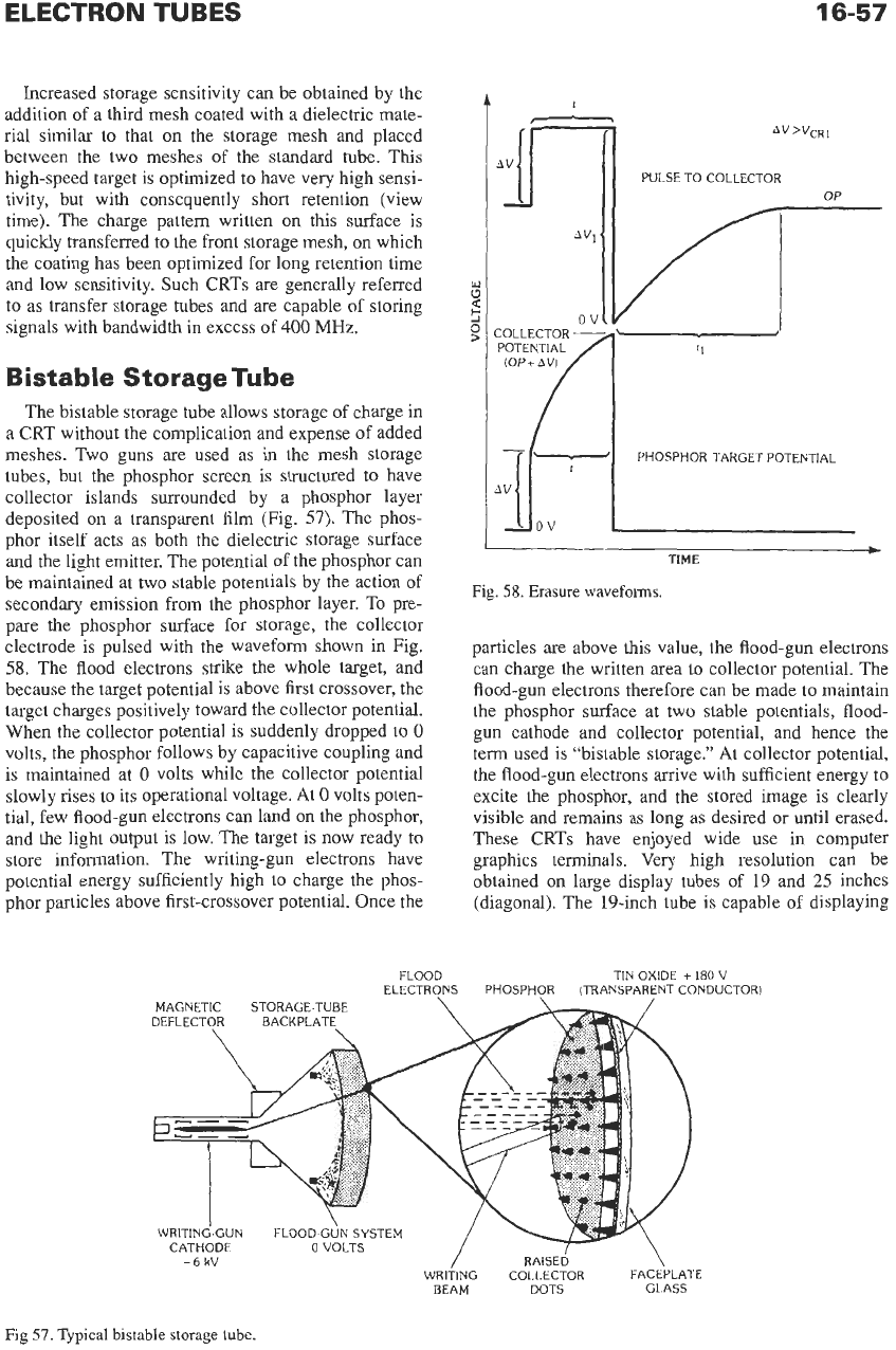
Fig.
54.
Magnetic deflection.
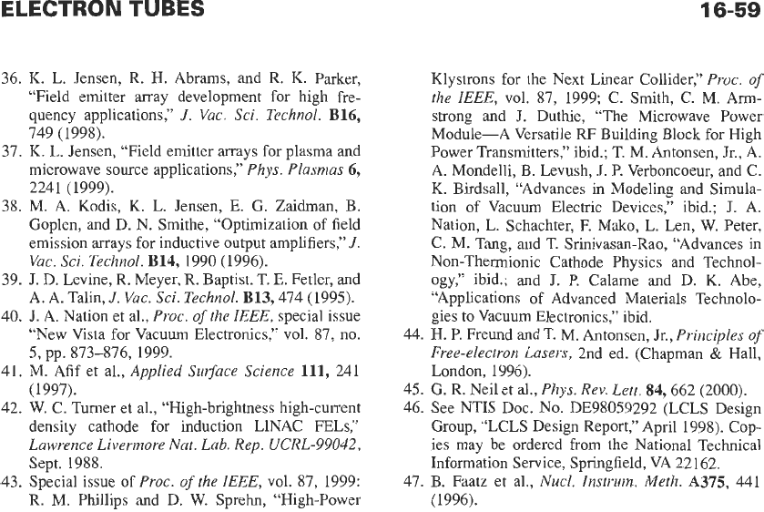
PHOSPHOR
VIEWING SCREEN
WRITING
CATHODE
I//
t&
p
FLOODING
CATHODE
BACKING
ELECTRODE
Fig.
56.
Construction of storage cathode-ray
tube.
I
I
Fig.
55.
Magnetic
focusing.
a
thin
dielectric material to form
a
surface on which
electrons store information.
A
typical storage tube is
shown in Fig.
56.
The writing gun emits
a
pencil-like electron beam,
which can be modulated by the information to be
stored. This information is in the form
of
an electrical
input signal that can be applied
to
the control grid for
intensity modulation or to the deflection electrodes for
spatial modulation. The storage surface is scanned by
this high-resolution beam, which actually strikes the
surface. A positive-charge image corresponding to the
input signal pattern is created on the storage surface by
secondary-emission effects. The image remains on the
storage surface until it decays from the neutralizing
action of gas ions or is erased intentionally. The stor-
age screen acts as
an
array of elemental electron guns,
with each mesh hole acting as
a
control element
of
one
of the guns. The desired information is stored on the
storage mesh by the action
of
the writing gun, and the
entire surface is flooded
by
electrons
from
the flood
gun. The value
of
the positive charge deposited at each
mesh aperture controls the amount
of
flood-gun
cur-
rent that can pass through the mesh aperture to the
phosphor screen. The current that passes through the
mesh strikes the phosphor, and light is emitted
in
pro-
portion to the current density arriving and to the land-
ing energy of the electrons.
In
other words, a gray
scale
is
reproduced in the stored image. After the
stored information has been observed or recorded, it is
erased from the storage surface by fully writing the
whole target first with high-energy flood electrons and
then with low-energy electrons. The net negative
charge
so
deposited on the storage target causes the
target to be maintained at flood-gun cathode potential.
The target is then prepared for storing a new image.
ELECTRON
TUBES
16-57
Increased storage sensitivity can be obtained by the
addition of a third mesh coated with a dielectric mate-
rial similar
to
that on the storage mesh and placed
between the two meshes of the standard tube. This
high-speed target is optimized
to
have very high sensi-
tivity, but with consequently short retention (view
time). The charge pattern written on
this
surface is
quickly transfened
to
the front storage mesh, on which
the coating has been optimized for long retention time
and low sensitivity. Such CRTs are generally referred
to as transfer storage tubes and are capable of storing
signals with bandwidth in excess of
400
MHz.
Bistable StorageTube
The bistable storage tube allows storage of charge in
a CRT without the complication and expense of added
meshes. Two guns are used as
in
the mesh storage
tubes, but the phosphor screen is structured to have
collector islands surrounded by a phosphor layer
deposited on a transparent film (Fig.
57).
The phos-
phor itself acts as both the dielectric storage surface
and
the
light emitter. The potential of the phosphor can
be maintained at two stable potentials by the action of
secondary emission from the phosphor layer. To pre-
pare the phosphor surface for storage, the collector
electrode is pulsed with the waveform shown in Fig.
58.
The flood electrons strike the whole target, and
because the target potential is above first crossover, the
target charges positively toward the collector potential.
When the collector potential is suddenly dropped to
0
volts, the phosphor follows by capacitive coupling and
is maintained at
0
volts while the collector potential
slowly rises to its operational voltage.
At
0
volts poten-
tial, few flood-gun electrons can land on the phosphor,
and the light output is low. The target is now ready to
store information. The writing-gun electrons have
potential energy sufficiently high to charge the phos-
phor particles above first-crossover potential. Once the
t
PULSE TO COLLECTOR
OP
/I
POTENTIAL
tl
7
1-1
PHOSPHOR TARGET POTENTIAL
4
I
I
ll0v
L
+
TIME
Fig.
58.
Erasure waveforms.
particles
are
above this value, the flood-gun electrons
can charge the written area to collector potential. The
flood-gun electrons therefore can be made to maintain
the phosphor surface at two stable potentials,
flood-
gun cathode and collector potential, and hence the
term used is “bistable storage.”
At
collector potential,
the flood-gun electrons arrive with sufficient energy to
excite the phosphor, and the stored image is clearly
visible and remains as long as desired or until erased.
These CRTs have enjoyed wide use in computer
graphics terminals. Very high resolution can be
obtained on large display tubes of 19 and
25
inches
(diagonal). The 19-inch tube is capable of displaying
FLOOD
TIN OXIDE
+
180
V
ELECTRONS PHOSPHOR (TRANSPARENT CONDUCTOR)
-6
kV
RAISED
WRITING
COLLECTOR FACEPLATE
BEAM
DOTS GLASS
Fig
57.
Typical
bistable storage tube.
8500
characters, and the 25-inch CRT is capable of
over
15
000
characters. Since these characters are
actually stored on the face
of
the CRT until erased, no
solid-state memory is required to refresh them.
Another advantage of this type of CRT
is
that when a
line is scanned with the writing gun at low beam cur-
rent, the collector current will be a function
of
whether
the area scanned is written or not. This signal current
can be amplified and processed to produce an elec-
tronic image of the written areas. This image can be
fed into a copy device for producing a hard copy of the
display.
REFERENCES
&.
3.
4.
5.
6.
7.
8.
9.
10.
11.
12.
13.
14.
15.
16.
17.
18.
1.
A.
S.
Gilmour, Jr.,
Microwave
Tubes (Artech
House, Inc., Nonvood, MA,
1986).
9
G.
A. Haas, A. Shih, and R.
E.
Thomas,
Applica-
tion
of
Suqace Science
2,293-321 (1979).
A.
Shih and G. A. Haas,
Appl.
Surf.
Sci.
2, 164-
172 (1979).
A. Shih and G. A. Haas,
Appl.
Surf.
Sci.
2, 275-
283 (1979).
A. M. Shroff, “Review of dispenser cathodes,”
Revue Technique Thomson-CSF
23, 947-1026
(1991).
C. R.
K.
Manian,
G.
A.Haas, and A. Shih,
Appl.
Surf: Sci.
24,391 (1985).
M. C. Green.
Technical Report RADC-TR-81-211,
July
1981.
TriService/NASA Cathode Life Test Facility
Annual Report, Naval Surface Warfare Center,
Crane Division, Crane
IN.
W.
Mueller,
IEEE Transactions on Electron
Devices
36, 180-187 (1989).
R. E. Thomas, J.
W.
Gibson, G. A. Haas, and
R.
H.
Abrams,
IEEE Transactions on Electron Devices
J. Hasker, J. van Esdonk, and J.
E.
Crombeen,
Appl. Surf: Sci.
26, 173 (1986).
G. Gartner, P. Geittner, H. Lydtin, and A. Ritz,
Appl. Surf: Sci.
111,
11 (1997).
S. M.
Sze,
Physics
of
Semiconductor Devices,
2d
ed. (Wiley, New York,
1981).
A. Modinos,
Field, Thermionic, and Secondary
Electron Emission Spectroscopy
(Plenum, New
York,
1984).
R. H. Fowler and L.
W.
Nordheim,
Proc. R.
SOC.
London
Ser.
A
119, 173 (1928).
E.
L. Murphy and R. H. Good,
Phys. Rev.
102,
1464 (1956).
C. A. Spindt,
I.
Brodie,
L.
Humphrey,
E.
R.
West-
erberg,
J.
Appl. Phys.
47,5248 (1976).
C. Bandis and
B.
B. Pate,
Appl. Phys. Lett
69, 366
37,850-861 (1990).
__.
21.
S.
T. Purcell,
V.
T. Binh,
R.
Baptist, “Nanoprotru-
sion model for field emission
from integrated
microtips,”
J.
Vac. Sci. Technol.
B15, 1666 (1997).
22.
W.
A.
Mackie, T. Xie, and P.
R.
Davis, “Transition
metal carbide field emitters for field-emitter array
devices and high current applications,”
J.
Vac. Sci.
Technol.
B17,613 (1999).
23.
W.
Zhu, C. Bower,
0.
Zhou,
G.
Kochanski, and
S.
Jin,Appl.
Phys. Lett.
75,875 (1999).
24.
J.
Robertson, “Field emission from carbon sys-
tems,”
Mat. Res. SOC. Symp. Proc.
Vol.
621
(Materi-
als
Research Society, Warrendale, PA,
2000),
R1.l.
25.
D. R. Whaley,
B.
M. Gannon,
C.
R. Smith, C.
M.
Armstrong, and
C.
A. Spindt, “Application
of
field
emitter arrays to microwave power amplifiers,”
IEEE Trans. Plas.
Sci.
28,727 (2000).
26.
K. L. Jensen, R. H. Abrams, and R.
K.
Parker,
“Field emitter array development for high fre-
quency applications,”
J.
Vac. Sci. Technol.
B16,
749 (1998).
27.
C.
M.
Marrese, J. E. Polk, K. L. Jensen, A. D. Gal-
limore, C. A. Spindt, R. L.
Fink,
and W. D. Palmer,
“Performance of field emission cathodes in xenon
electric propulsion system environments,” chapter
11
in
Micropropulsion
for
Small Spacecraft
(Vol.
187
of Progress in Astronautics and Aeronautics),
M.
M.
Micci, A.
D.
Ketsdever (eds.) (American
Institute of Aeronautics and Astronautics, Reston,
VA,
2000).
28.
A.
Ghis, R. Meyer,
P.
Rambaud,
F.
Levy, and T.
Leroux, “Sealed vacuum devices-Fluorescent
microtip displays,”
IEEE Trans. Electron. Devices
38,2320 (1991).
29.
A. A. Talin, K. A. Dean, and J. E. Jaskie, “Field
emission displays: A critical review,” to appear in
Vacuum Microelectronics:
A
Special Issue
of
Solid
State Electronics
(2001).
30.
D.
W.
Jenkins, “Emission area of a field emitter
array,”
IEEE Trans. Electron. Devices
40,
666
(1993).
31.
R.
L.
Hartman,
W.
A. Mackie, and P. R. Davis,
“Use
of
boundary element methods in field emis-
sion computations,”
J.
Vac. Sci. Technol.
B12, 754
(1994).
32.
K. L. Jensen, “Field emitter arrays for plasma and
microwave source applications,”
Phys. Plasmas
6,
2241 (1999).
33.
C. Constancias and R. Baptist, “Emission observa-
tion of a microtip cathode array with an electro-
static-lens projector: Statistical approach,”
J.
Vac.
Sci. Technol.
B16,841 (1998).
34.
R. Schlesser,
M.
T. McClure, B.
L.
McCarson, and
Z.
Sitar, “Bias voltage dependent field-emission
energy distribution analysis of wide band-gap field
emitters,”
J.
Appl. Phys.
82,5763 (1997).
(
19
Y
6).
35.
C.
A. Spindt, C.
E.
Holland,
P.
R. Schwoebel, and
I.
Brodie, “Field-emitter-array development for
microwave applications,”
J.
Vac. Sci. Technol.
B14, 1986 (1996).
19.
R. Stratton,
Phys. Rev.
135, A794 (1964).
20.
C. A. Spindt,
I.
Brodie,
L.
Humphrey, E. R. West-
erberg,
J.
Appl. Phys.
47,5248 (1976).
36. K. L. Jensen,
R.
H.
Abrams, and R. K. Parker,
“Field emitter array development for high fre-
quency applications,”
J.
Vac. Sci. Technol.
B16,
749 (1998).
37. K. L. Jensen, “Field emitter arrays for plasma and
microwave source applications,”
Phys. Plasmas
6,
2241 (1999).
38.
M. A. Kodis, K. L. Jensen, E. G. Zaidman, B.
Goplen, and D. N. Smithe, “Optimization of field
emission arrays for inductive output amplifiers,”
J.
Vac. Sci. Technol.
B14, 1990 (1996).
39. J. D. Levine,
R.
Meyer, R. Baptist, T. E. Fetler, and
A. A. Talin,
J.
Vac. Sci. Technol.
B13,474 (1995).
40. J. A. Nation et
al.,
Proc.
of
the
IEEE,
special issue
“New Vista for Vacuum Electronics,” vol. 87,
no.
41.
M. Afif et al.,
Applied Surface Science
111,
241
(1997).
42.
W.
C. Turner et al., “High-brightness high-current
density cathode for induction LINAC
FELs,”
Lawrence Livermore Nat. Lab. Rep. UCRL-99042,
Sept. 1988.
43. Special issue of
Proc.
of
the
IEEE,
vol. 87, 1999:
R.
M. Phillips and D.
W.
Sprehn, “High-Power
5,
pp. 873-876, 1999.
Klystrons for the Next Linear Collider,”
Proc.
of
the
IEEE,
vol. 87, 1999; C. Smith, C.
M.
Arm-
strong and J. Duthie, “The Microwave Power
Module-A Versatile
RF
Building Block for High
Power Transmitters,” ibid.; T. M. Antonsen, Jr., A.
A.
Mondelli, B. Levush,
J.
P. Verboncoeur, and C.
K. Birdsall, “Advances
in
Modeling and Simula-
tion of Vacuum Electric Devices,” ibid.;
J.
A.
Nation, L. Schachter, F. Mako, L. Len,
W.
Peter,
C. M. Tang, and T. Srinivasan-Rao, “Advances in
Non-Thermionic Cathode Physics and Technol-
ogy,” ibid.; and
J.
P.
Calame and
D.
K.
Abe,
“Applications of Advanced Materials Technolo-
gies to Vacuum Electronics,” ibid.
44.
H.
P. Freund and T.
M.
Antonsen, Jr.,
Principles
of
Free-electron Lasers,
2nd ed. (Chapman
&
Hall,
London, 1996).
45. G.
R.
Neil et
al.,
Phys. Rev. Lett.
84,662 (2000).
46. See NTIS Doc. No. DE98059292 (LCLS Design
Group, “LCLS Design Report,” April 1998). Cop-
ies may be ordered from the National Technical
Information Service, Springfield, VA 22162.
47. B. Faatz et
al.,
Nucl. Instrum. Meth.
A375
441
(1996).

Power
Grid-Tub
e
Circuits
Mawin Chodorow and Donald
H.
Preist
General Design
17-2
Graphic Design Methods
17-4
Class-C RF Amplifier or Oscillator
Class-B RF Amplifiers
Class-A and -AB AF Amplifiers
Class-AB and -B AF Amplifiers
Circuit Classification
17-8
RF Amplifier Circuits
17-8
Triodes
Tetrodes and Pentodes
UHF Operation
KlystrodeTM Amplifiers
Circuits
of
Special Interest
Performance
of
Electron Power Tubes; Comparison With Solid-state
Devices
17-13
Power Gain and Bandwidth
of
RF Amplifiers
Power Output Under Pulse Conditions
Life Expectancy
of
Tubes
Development Trends in Gridded Power Tubes
17-1
17-2
REFERENCE
DATA
FOR ENGINEERS
It is common practice to differentiate between types
of vacuum-tube circuits, particularly amplifiers, on the
basis
of
the operating regime of the tube.
CZuss-A:
Grid bias and alternating grid voltages such
that plate current flows continuously throughout electri-
cal cycle
(ep
=
360").
CZass-AB:
Grid bias and alternating grid voltages
such that plate current flows appreciably more than half
but less than entire electrical cycle (360"
>
Op
>
180").
Class-B:
Grid bias close
to
cutoff such that plate
current flows only during approximately half
of
electri-
cal
cycle
(
Op
7
180").
Class-C:
Grid bias appreciably greater than cutoff
so
that plate current flows for appreciably less than half of
electrical cycle
(
Op
<
180").
A
further classification between circuits in which
positive grid current is conducted during some portion
of the cycle and those in which it is not is denoted by
subscripts
2
and
1,
respectively. Thus
a
class-AB,
amplifier operates with
a
positive swing of the alternat-
ing grid voltage such that positive electronic current is
conducted and accordingly in-phase power is required
to drive the tube.
GENERAL DESIGN
For quickly estimating the performance of
a
tube
from catalog data, or for predicting the characteristics
needed for
a
given application, the ratios given below
may be used.
Table 1 gives correlating data for typical operation of
tubes in the various amplifier classifications. If the
maximum ratings of
a
tube are known, the maximum
power output, currents, voltages, and corresponding
load impedance may be estimated from the table. Take
for example
a
type F- 124-A water-cooled transmitting
tube operated
as
a
class-C radio-frequency power ampli-
fier and oscillator (the constant-current characteristics
are shown in Fig. 1). Published maximum ratings are
as
follows.
Dc grid voltage:
E,
=
3000 volts
Dc plate current:
Ib
=
7
amperes
RF
grid current:
I,
=
50
amperes
Plate input:
P,
=
135
000
watts
Plate dissipation:
Pp
=
40
000
watts
Maximum conditions may be estimated
as
follows.
For
77
=
75
percent
P,
=
135
000
watts
E,
=
20
000
VOkS
Power output
Po
=
qc
=
100
000
watts.
Average dc plate current
Ib
=
P,/Eb
=
6.7
amperes
From
a
tabulated typical ratio
Mib/Ib
=
4,
the
instantaneous peak plate current
Mib
=
41,
=
27
amperes.
*
The rms plate alternating-current component, taking
the ratio
Ip/Ib
=
1.2,
is
Ip
=
1.21,
=
8
amperes
The rms value of the plate alternating-voltage compo-
nent from the ratio
Ep/Eb
=
0.6
is
Ep
=
0.6
E,
=
12
000 volts.
Dc plate voltage:
*
In
this discussion, the superscript
M
indicates the use
of
the maximum or peak value of the varying component; i.e.,
=
maximum
or
peak value
of
the alternating component
of the plate current.
TABLE 1. TYPICAL AMPLIFIER OPERATING DATA (MAXIMUM-SIGNAL CONDITIONS,
FER
TUBE)
~~~ ~
Function
Plate efficiency
17
(percent)
Peak instantaneous
to
dc plate-current
Rms alternating to dc plate-current
Rms alternating to dc plate-voltage
Dc
to peak instantaneous grid-current
ratio
Mib~~b
ratio
IpiIb
ratio
EpIEb.
IpIMi?
~
Class
B
Class
A
AF
(P-P)
20-30
35-65
1.5-2
3.1
0.5-0.7 1.1
0.3-0.5 0.5-0.6
0.1-0.25
~
Class
B
RF
Class C
RF
60-70
3.1
1.1
0.5-0.6
0.1-0.25
65-85
3.1-4.5
1.1-1.2
0.5-0.6
0.1-0.25
POWER
GRID-TUBE
CIRCUITS
17-3
GRID
AMPERES
i,
PLATE
KILOVOLTS
eb
Fig.
1.
Constant-current characteristics
of
type
F-124-A
tube
with
typical load lines: AB-class C, CD-class
B,
EFG-class
A,
HJK-class
AB.
The approximate operating load resistance,
R
j,
is
now found from
R,
=
EPMp
=
1500
ohms
An estimate of the grid drive power required may be
obtained by reference
to
the constant-current
characteristics of the tube and determination of the peak
instantaneous positive grid current
Mi,
and the corre-
sponding instantaneous total grid voltage
Mec.
If the
value of grid bias for the given operating condition is
E,,
the peak alternating grid drive voltage is
ME,
=
(Mec
-
E,)
from which the peak instantaneous grid drive power can
be determined:
MPc
=
MEgMic
An
approximation to the average grid drive power,
P,,
necessarily rough due to neglect
of
negative grid
current,
is
obtained from the typical ratio of dc to peak
value
of
grid current,
ZJMi,
=
0.2.
The result is
P,
=
ICE,
=
0.2MicE,
watt
Plate dissipation
Pp
may be checked with published
values since
Pp
=
Pi
-
Po
It should be borne in mind that combinations of
published maximum ratings
as
well
as
each individual
maximum rating must be observed. Thus, for example
in this case, the maximum dc plate operating voltage of
20
000
volts does not permit operation at the maximum
dc plate current
of
7
amperes since this exceeds the
maximum plate input rating of
135
000
watts.
Plate load resistance
R
may be connected directly in
the tube plate circuit as in the resistance-coupled
amplifier, through impedance-matching elements
as
in
audio-frequency transformer coupling, or effectively
represented by a loaded parallel-resonant circuit as in
most radio-frequency amplifiers. In any case, calculated
values apply only
to
effectively resistive loads, such
as
are normally closely approximated in radio-frequency
amplifiers. With appreciably reactive loads, operating
currents and voltages will in general be quite different,
and their precise calculation is quite difficult.
The physical load resistance present in any given
setup may be measured by audio-frequency or radio-
frequency bridge methods. In many cases, the proper
value
of
Rl
is ascertained experimentally
as
in radio-
frequency amplifiers that are tuned to the proper
minimum dc plate current. Conversely, if the circuit is
to be matched to the tube,
R,
is determined directly
as
in a resistance-coupled amplifier or as
Rj
=
N2R,
in the case of
a
transformer-coupled stage, where
N
is
the primary-to-secondary voltage transformation ratio.
17-4
REFERENCE DATA FOR ENGINEERS
In a parallel-resonant circuit in which the output resist-
ance
R,
is connected directly in one of the reactance
legs
R,
=
X21R,
=
LlCu,
=
QX
where,
X
is the leg reactance at resonance (ohms),
L
and
C
are leg inductance in henrys and
Q
=
XIR,.
capacitance in farads, respectively,
GRAPHIC DESIGN METHODS
When accurate operating data are required, more
precise methods must be used. Because of the nonlinear
nature of tube characteristics, graphic methods usually
are most convenient and rapid. Examples of such
methods are given below.
A
comparison of the operating regimes of class
A,
AB,
B, and C amplifiers is given in the constant-
current-characteristics graph of Fig. 1. The lines corre-
sponding to the different classes of operation are the loci
of instantaneous grid voltage
e,
and plate voltage
e,,,
corresponding to their respective load impedances.
For radio-frequency amplifiers and oscillators having
tuned circuits that give an effectively resistive load, plate
and grid tube and load alternating voltages are sinusoi-
dal and in phase (disregarding transit time), and the loci
become straight lines.
For amplifiers having nonresonant resistive loads, the
loci are in general nonlinear except in the distortionless
case of linear tube characteristics (constant
rP),
for
which they are again straight lines.
Thus, for determination of radio-frequency perform-
ance, the constant-current chart
is
convenient.
For
solution of audio-frequency problems, however, it
is
more convenient to use the
ib-ec
transfer characteristics
of Fig.
2,
on which a dynamic load line may be
constructed.
Methods for calculation
of
the most important cases
are given below.
Class-C RF Amplifier
or
Oscillator
Draw a straight line from
A
to
B
(Fig.
1)
correspond-
ing
to
the chosen dc operating plate and grid voltages,
and to the desired peak alternating plate and grid
voltage excursions. The projection of
AB
on the hori-
zontal axis thus corresponds
to
"Ep:
Using ChaEee's
1
1-point method of harmonic analysis, lay out on
AB
points
ep'
=
"Ep
epll
=
0.866ME,
epln
=
0.5'Ep
TOTAL
GRID
VOLTS
e,
FOR
TUBE
I
-1200 -1000 -800 -600 -400 -200 0 200 400 600 800
10
5
P
v1
K
30
e
5
L
5
10
800 600 400
200
0
-200 -400
-600
-800 -1000 -1200
TOTAL
GRID
VOLTS
e,
FOR
TUBE
I1
1000 800
600
400 200 0
200
400 600 800 1000
AC
GRID
VOLTS
eg
I
Fig.
2.
Transfer characteristics
ib
versus
e,
with load lines: CKF-class
A,
and
OPL-class E.
POWER GRID-TUBE CIRCUITS
17-5
to each of which correspond instantaneous plate cur-
rents,
ib',
it,
and
ir
and instantaneous grid currents
z,
,
i,",
and
i/.
The operating currents are obtained
from
'I
Ib
=
[ib'
+
2i,"
+
2i,"']/12
I,
=
[i,'
+
2i,"
+
2i,"']/12
MIP
=
[ib'
+
1.73i;
+
i,"']/6
MI,
=
[i,'
+
1.73i,"
+
i,"']l6
Substitution of the above in the following gives the
desired operating data.
Power output
Po
=
("EpMIp)/2
Power input
Pi
=
EbIb
Average grid excitation power
Pg
=
('EgMI,)12
Peak grid excitation power
MP,
=
Plate load resistance Rl
=
MEp/MIp
Grid bias resistance
R,
=
EJI,
Plate efficiency
7
=
Polpi
Plate dissipation
Pp
=
Pi
-
Po
The above procedure may also be applied to plate-
modulated class-C amplifiers. Take the above data as
applying to carrier conditions, and repeat the analysis
for
'IestEb
=
2Eb
and
crestPo
=
4P0,
keeping Rl constant.
After a cut-and-try method has given a peak solution, it
will often be found that combination fixed and self grid
biasing as well as grid modulation are indicated to
obtain linear operation.
To illustrate the preceding exposition, a typical
amplifier calculation is given below.
Operating requirements (carrier condition):
E,
=
12
000
Volts
Po
=
25
000
watts
7
=
75
percent
Preliminary calculation (refer to Tables
1
and
2):
Ep/Eb
=
0.6
Ep
=
0.6
X
12
000
=
7200
volts
MEP
=
1.41
X
7200
=
10
000
volts
Ip
=
PolEp
25
00017200
=
3.48
amperes
M~P
=
4.9
amperes
tp&
=
1.2
Ib
=
3.4811.2
=
2.9
amperes
Pi
=
12
000
X
2.9
=
35
000
watts
Mib/Ib
=
4.5
=
4.5
X
2.9
=
13.0
amperes
R,
=
EplIp
=
720013.48
=
2060
ohms
Complete Calculation:
Lay out carrier operating line
AB
on the constant-current graph, Fig.
1,
using values
of
Eb, MEp,
and
Mib
from the preliminary calculated
data. Operating carrier bias voltage
E,
is chosen some-
what greater than twice the cutoff value
(1000
volts) to
locate point A.
The following data are taken along
AB.
ib'
=
13
amperes
i/
=
10
amperes
TABLE
2.
CLASS-c
RF
AMPLIFIER
DATA
FOR
100-PERCENT PLATE
MODULATION
Detailed
Preliminary
Symbol
Carrier Carrier Crest
E,
(Volts) 12
000
12
000
24
000
MEp
(volts) 10
000
10
000
20
000
M~P
(amperes)
4.9
5.1
10.2
-1
000
-
700
ME,
(volts)
-
1
740
1
740
I,
(amperes)
2.9
2.8
6.4
I,
(amperes)
-
0.125
0.083
M~,
(amperes)
-
0.255
0.183
P,
(watts) 35
000
33
600
154
000
Pg
(watts)
-
220 160
7
(percent)
75 76
66
Rl
(ohms) 2
060
1960 1
960
R,
(ohms)
-
7
100
7
100
E,,
(volts)
-
-110 -110
E,
(volts)
-
Po
(watts) 25
000
25
500
102
000