Middleton W.M. (ed.) Reference Data for Engineers: Radio, Electronics, Computer and Communications
Подождите немного. Документ загружается.

17-16
REFERENCE
DATA
FOR ENGINEERS
k
“sk
TIME
V,k
=
Anode-cathode voltage
Vg+=
Grid-cathode voltage
io
=Anode current
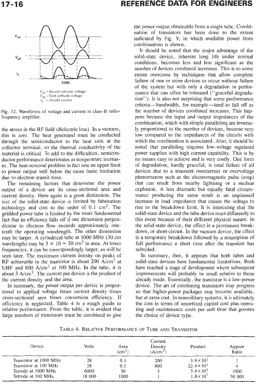
Fig. 12. Waveforms
of
voltage
and
current
in class-B radio-
frequency amplifier.
the atoms in the RF field (dielectric loss). In a vacuum,
this is zero. The heat generated must be conducted
through the semiconductor to the heat sink at the
collector terminal,
so
the thermal conductivity of the
material is critical. To add to the difficulties, semicon-
ductor performance deteriorates as temperature increas-
es. The heat-removal problem in fact sets an upper limit
to power output well below the more basic limitation
due to electron transit time.
The remaining factors that determine the power
output of a device are its cross-sectional area and
current density. Here again
is
a great distinction. The
size of the solid-state device is limited by fabrication
technology and cost to the order of
0.1
cm2. The
gridded power tube is limited by the more fundamental
fact that its efficiency falls
off
if one dimension perpen-
dicular to electron flow exceeds approximately one-
tenth the operating wavelength. The other dimension
may be larger. A cylindrical tube at
1000
MHz
(30
cm
wavelength) may be
3
X
10
=
30
cm2 in area. At lower
frequencies, it can be correspondingly larger, as will be
seen later. The maximum current density on peaks of
RF achievable in the transistor is about
200
Ncm2 at
UHF
and
800
Ncm2 at
100
MHz.
In the tube, it is
about
3
Ncm2. The current per device is the product of
the current density and the area.
In summary, the power output per device is propor-
tional
to
applied voltage times current density times
cross-sectional area times conversion efficiency. If
efficiency is neglected, Table
4
is a rough guide to
relative performance. From the table, it is evident that
large numbers
of
transistors must be combined to give
TABLE
4.
RELATIVE
PERFORMAN(
the power output obtainable from a single tube. Combi-
nation of transistors has been done to the extent
indicated by Fig.
9,
in which available power from
combinations is shown.
It
should be noted that the major advantage of the
solid-state device, inherent long life under normal
conditions, becomes less and less significant as the
number
of
devices combined increases. This is to some
extent overcome by techniques that allow complete
failure of one or more devices to occur without failure
of the system but with only a degradation in perfor-
mance that can often be tolerated (“graceful degrada-
tion”).
It
is also not surprising that some performance
criteria-bandwidth, for example-tend to fall off as
the number of devices combined increases. This hap-
pens because the input and output impedances of the
combination, which with simple paralleling are inverse-
ly proportional to the number of devices, become very
low compared to the impedances of the circuits with
which the combination is associated.
Also,
it should be
noted that paralleling requires low-voltage regulated
power supplies with high current capability. This
is
by
no means easy to achieve and is very costly. One form
of degradation, hardly graceful, is total failure
of
all
devices due to a transient overcurrent or overvoltage
phenomenon such as the electromagnetic pulse (emp)
that can result from nearby lightning or a nuclear
explosion.
A
less dramatic but equally fatal circum-
stance producing the same result is an unplanned
increase in load impedance that causes the voltage to
rise to the breakdown limit. It is interesting that the
solid-state device and the tube device react differently
to
this event because of their different physical nature. In
the solid-state device, the effect
is
a permanent break-
down, or short-circuit. In the vacuum device, the effect
is a temporary breakdown followed by a resumption of
full performance a short time after the transient has
subsided.
In summary, then, it appears that both tubes and
solid-state devices have fundamental limitations. Both
have reached a stage of development where subsequent
improvements will probably be small relative to those
already made. Essentially, the transistor
is
a low-power
device. The art of combining transistors may progress
so
that higher-power packages may become available,
but at extra cost. In nonmilitary systems, it is ultimately
the cost in terms
of
amortized capital cost plus opera-
ting and maintenance costs per unit time that governs
the choice of device type.
:E
OF
TUBE
AND
TRANSISTOR
Device
~ ~~~
Current
(4
(A/cm2)
Volts
Area
Density
Product
Approx
Ratio
Transistor
at
1000
MHz
28
0.1
200
5.6X
102
1
Transistor
at
100
MHz
28
0.1
800
22.4X
10’
4
Tetrode
at
1000 MHz
6000
30
3
5.4X10⁵
1000
Tetrode
at
100
MHz
18
000
1000
1
1.8X10⁷
30
000
POWER GRID-TUBE CIRCUITS
17-17
(It is of historical interest that before the advent of
high-power velocity-modulated tubes, serious and suc-
cessful attempts were made to combine triodes and
tetrodes to increase RF power output at VHF and UHF,
and many transmitters were built this way. As soon as
tubes giving sufficient power from
a
single type for the
application became available, these multitube equip-
ments were superceded for economic reasons
.)
Power Gain and Bandwidth of
RF Amplifiers
Power gain and bandwidth of RF amplifiers depend
on both device and circuit properties. As noted above,
the power gain of
a
tetrode falls in the range between
30
dB at LF and MF and
10
dB at UHF. Power gain at
UHF is limited by electron-transit-time effects and by
the inevitable effect of cathode-lead inductance.
Corresponding bandwidths with conventional reso-
nant circuits fall between about
1%
(AM broadcast,
UHF TV) and
10%
(TV at
50
MHz) of the carrier
frequency.
For a simplified ideal tube amplifier, the gain-
bandwidth product tends to be constant and equal to
G,IC,
where
G,
is the mutual conductance (transcon-
ductance) and
C
is the output capacitance. This product
is independent of frequency. In practice, the product is
always less because of the presence of the external
circuits that store energy and because the bandwidth of
the input circuit may be smaller than that of the output
circuit. Furthermore, the performance of the amplifier
may be largely determined by the amount of feedback
present. It is nevertheless true that the gain-bandwidth
product will always increase with
G,IC.
This factor is related to interelectrode spacings and is
approximately inversely proportional to the grid-
cathode spacing. The achievement of small spacing,
which implies fine grid wires and structures of high
dimensional stability with respect to change of tempera-
ture, has always been a major challenge in tube design.
Power Output Under Pulse
Conditions
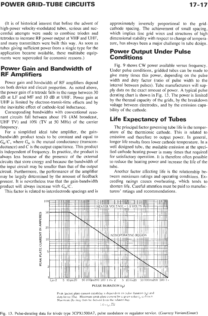
Fig.
9
shows CW power available versus frequency.
Under pulse conditions, gridded tubes can be made to
give many times this power, depending on the pulse
width and duty factor (ratio of pulse width to the
interval between pulses). Tube manufacturers will sup-
ply data on the exact amount of power. A typical pulse
derating chart is shown in Fig.
13.
The power is limited
by the thermal capacity of the grids, by the breakdown
voltage between electrodes, and by the emission capa-
bility
of
the cathode.
Life Expectancy of Tubes
The principal factor governing tube life is the temper-
ature of the thermionic cathode. This is related to
emission and therefore to output power. In general,
longer life results from lower cathode temperature. In a
well designed tube, the available emission at the speci-
fied cathode heating power is many times that required
for satisfactory operation. It is therefore often possible
to reduce the heating power and increase the life of the
tube.
Another factor affecting life is the relationship be-
tween maximum ratings and operating conditions. Ex-
ceeding ratings causes overheating, which tends to
shorten life. Careful attention must be paid
to
manufac-
turers’ ratings and recommendations.
PULSE
DURATION
(t,)
Peak
(pulse)
plate-current capability
is
dependent
on
pulse duration
(tp)
and
duty
factor
(Du)
Maximum
Du
may
then
be
derived
from
the
relationship.
Maximum
peak plate current
for
a
given value
tp
1s
.hewn
1
0=ab,E
Fig.
13.
Pulse-derating data for triode
type
3CPX1500A7,
pulse
modulator
or
regulator
service.
(Courtesy
VarianlEimac)
17-18
REFERENCE DATA FOR ENGINEERS
Life expectancy for a highly stressed oxide-cathode
tube at UHF may be 2500 hours. For a thoriated-
tungsten-filament tube in broadcast service, 50
000
hours
is
not uncommon.
Development Trends in Gridded
Power Tubes
Improved performance of power grid tubes, including
longer life, can be anticipated from the incorporation of
improved materials and fabrication techniques. For
example, the use
of
pyrolytic graphite for grids is
becoming standard practice. Impregnated tungsten dis-
penser cathodes commonly found in microwave
velocity-modulated tubes may find their way into
gridded power tubes.
In addition, improved structural forms such as modu-
lar
construction may allow the manufacture
of
very-
high-power tubes (capable of
10
MW
of
CW power
output) having higher gain-bandwidth products because
of smaller grid-cathode spacings.
At VHF and UHF, developments of the KlystrodeTM
amplifier may appear in applications where the combi-
nation of small size compared to a klystron; relatively
high efficiency, especially with amplitude modulation;
high power capability; and interesting power gain makes
it more attractive than a klystron or a conventional
tetrode.
REFERENCES
1. Tyler,
V.
J.
“A New High-Efficiency Power Ampli-
fier.”
Marconi Review,
Vol. 21, No. 130
(1958),
pp.
6-109.
2. Doherty, W. H. “A New High-Efficiency Power
Amplifier for Modulated Waves.”
Proc. IRE,
Vol.
24 (Sept. 1936), p. 1163.
3.
Terman,
F.
E.
Radio Engineers Handbook.
New
York: McGraw-Hill
Book
Co., 1943; pp. 455-458.
4.
Swanson, H. “The Pulse Duration Modulator, a
New Method
of
High Level Modulation in Broadcast
Transmitters.
”
IEEE Trans.
on
Broadcasting,
Vol.
BC17, No. 4 (Dec. 1971), pp. 89-92.
5. Ginzton, Hewlett, Jasberg, and Noe. “Distributed
Amplifications.”
Proc. IRE,
1948,
pp.
956-969.
18
Semiconductors
and Transistors
Ben G.
Streetman
Semiconductors
18-2
Semiconductor Materials
Energy Bands and Charge Carriers
Carrier Concentrations
Drift
of
Carriers
Excess Carriers; Diffusion
pn Junctions
18-8
A
Junction at Equilibrium
Forward and Reverse Bias
Reverse Breakdown
Capacitance and Transient Behavior
Diodes and Rectifiers
18-12
Transistors
18-13
Junction Field-Effect Transistors
MOS
Field-Effect Transistors
Bipolar Junction Transistors
Other Electronic Devices
18-21
Display
Devices
Microwave Devices
Switching Devices
18-1
18-2
REFERENCE DATA FOR ENGINEERS
The basic building blocks of any electronic circuit or
system are electronic devices-the transistors, diodes,
and other elements that collectively allow the system
to
perform its function. These devices may be individual
transistors, diodes, and passive elements soldered in
appropriate interconnection. Or, the system may be a
collection of complex integrated circuits, each com-
posed of thousands of active and passive elements on a
silicon chip (see Chapter
20).
The system may even
involve information transfer by a modulated light beam
and detector (see Chapter
21).
In any case, a great
variety of electronic elements is available for perform-
ing the desired function, and those who design or use
electronic equipment have a wide range of devices from
which
to
choose.
Most modern electronic devices are made with semi-
conductor materials. The unusual properties of these
solids are responsible for a revolution in electronics
since the invention of the transistor. This chapter* deals
with semiconductors and their applications in pn junc-
tions, transistors, and other devices. Circuit models of
transistors are discussed in Chapter
19,
and fabrication
methods are discussed in Chapter
20.
SEMICONDUCTORS
Semiconductors are a group of materials that have
electrical conductivities intermediate between those
of
metals and insulators. It is significant that the conduc-
tivity of these materials can be varied considerably by
changes in temperature, optical excitation, and impurity
content. This variability of electrical properties makes
possible the wide range
of
modern electronic devices.
*Much
of
this discussion is from Ben G. Streetman,
Solid
State Electronic Devices,
3rd ed.,
0
1990.
Reprinted by
permission
of
Prentice-Hall, Inc., Englewood Cliffs,
N.
J.
Semiconductor Materials
Semiconductors are found in column IV and neigh-
boring columns of the periodic table (Table
1).
The
column-IV semiconductors silicon (Si) and germanium
(Ge) are called
elemental
semiconductors because they
are composed of single species of atoms. In addition to
the elemental materials, compounds
of
column-I11 and
column-V atoms, as well as certain combinations from
columns I1 and VI, make up the
intermetallic,
or
compound,
semiconductors.
As Table 1 indicates, there are numerous semicon-
ductor materials. Among these, silicon is used for the
majority of semiconductor devices; rectifiers, transis-
tors, and integrated circuits are now made mostly in
silicon, although GaAs is also used in high-speed
integrated circuits. The compounds are most widely
used in devices requiring the emission
or
absorption of
light. For example, semiconductor light-emitting diodes
commonly are made of such compounds as GaAs, Gap,
and alloys such as GaAsP. An important microwave
device, the gunn diode, is usually made
in
GaAs. Thus,
the wide range of semiconductor materials offers con-
siderable variety in properties and provides experts in
electronic circuits and systems with much flexibility in
the design of electronic functions.
The electronic and optical properties
of
semiconduc-
tor materials are strongly affected by impurities, which
may be added in precisely controlled amounts. Such
impurities are used to vary the conductivities
of
semi-
conductors, and even
to
alter the nature
of
the conduc-
tion processes from conduction by negative charge
carriers to conduction by positive charge carriers. For
example, an impurity concentration of one part per
million can change a sample of silicon from a poor
conductor to a good conductor of electric current. This
process of controlled addition of impurities, called
doping,
will be discussed below.
TABLE
1.
COMMON SEMICONDUCTOR MATERIALS
The Portion
of
the Periodic Table Where Semiconductors Occur
I1 I11 IV V
Zn
Cd
B
C
AI Si P
Ga Ge As
In Sb
Elemental and Compound Semiconductors
Elemental IV Compounds 111-V Compounds
Si
Ge
Sic
SiGe
AIP
AlAs
AlSb
GaP
GaAs
GaSb
InP
InAs
InSb
VI
S
Se
Te
11-VI Compounds
ZnS
ZnSe
ZnTe
CdS
CdSe
CdTe
SEMICONDUCTORS AND TRANSISTORS
18-3
Virtually all semiconductor devices require single
crystals of extremely pure materials. Since small con-
centrations of impurities can radically alter their electri-
cal properties, device-grade semiconductor crystals are
grown with greater perfection than any other materials.
Energy Bands and Charge
Carriers
The atomic arrangement in most semiconductor
crystals is similar to the diamond lattice, in which each
atom is surrounded by four nearest neighbors. The
atomic bonding in the crystal is largely covalent (as in
the
H,
molecule). That
is,
the sharing of electrons
between adjacent atoms in covalent bonds holds the
crystal together. In the column-IV semiconductor sili-
con, for example, each atom has four valence electrons
shared with four nearest neighbors.
Electrons in isolated atoms are restricted to certain
discrete energy levels, predictable generally from the
Bohr model and more precisely from the results of
quantum mechanics.
In
a similar fashion, electrons in
solids are restricted to certain energies and are not
allowed at other energies. The basic difference between
the case of an electron in a solid and that of an electron
in an isolated atom is that in the solid the electron has a
range,
or
band,
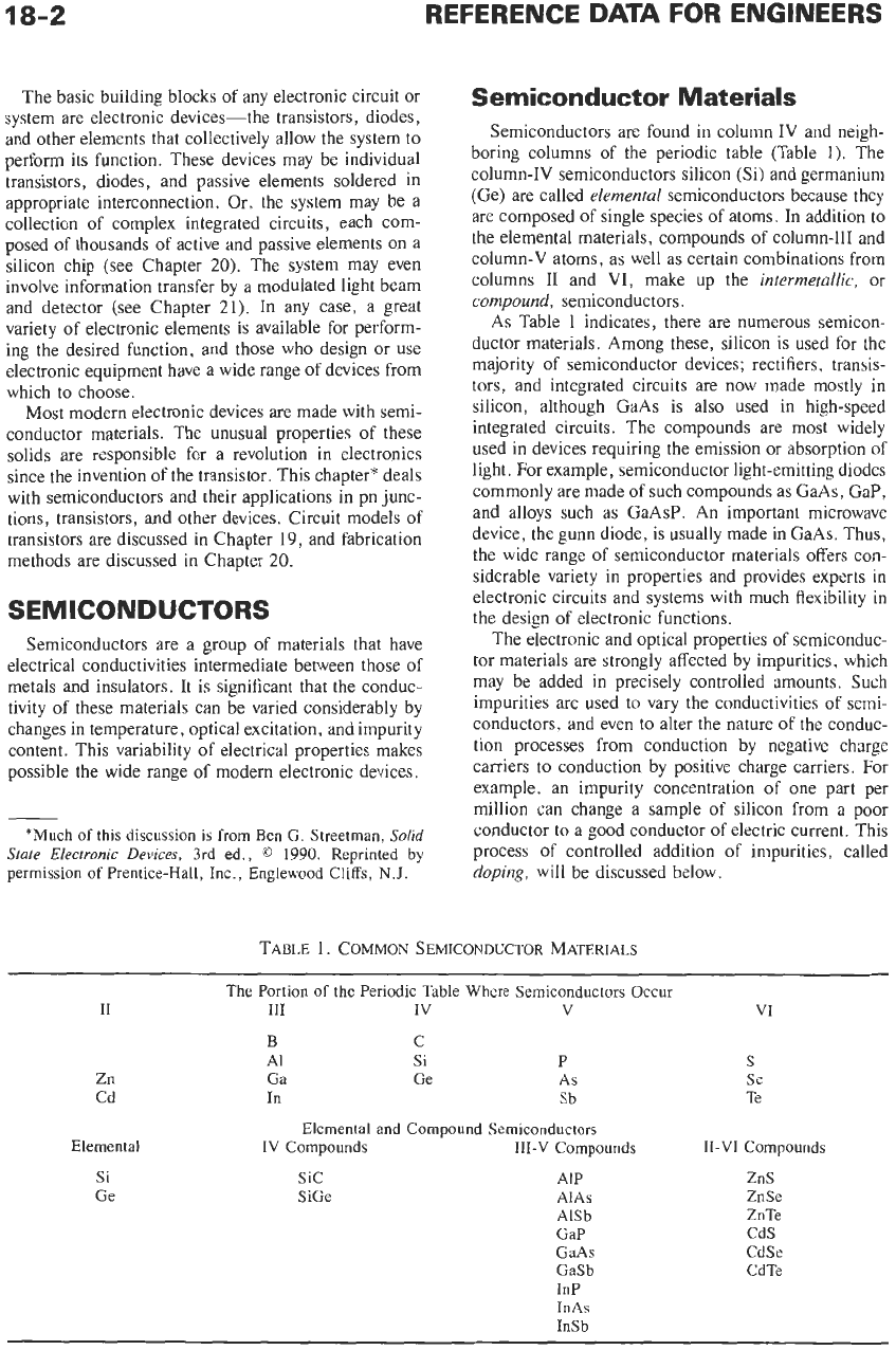
of available energies. General features
of the energy bands for insulators, metals, and semi-
conductors are shown in Fig.
1.
In
an insulator or
semiconductor, a lower (valence) band is filled with
electrons at low temperatures, and an upper (conduc-
tion) band is empty of electrons. The separation be-
tween the valence and conduction bands is called the
band
gap
E,.
Insulators have a wider band gap than do
semiconductors, and metals have overlapping bands.
The variety of electrical conductivities of metals,
insulators, and semiconductors arises primarily from
their band structures (Fig.
1).
If electrons are to
experience acceleration in an electric field, they must be
able to move into new energy states.
In
a completely
filled band, there are
no
available empty states, and
therefore
no
net charge transport
(no
current) can take
place. The same is true for an empty band, which
contains
no
electrons to move. As a result, a perfect
insulator does not conduct current. Metals,
on
the other
hand, have electrons mixed with unfilled allowable
CONDUCTION
1
COhDUCTION
i
OVERLAP
VALENCE
VALENCE
(A)
Insdotor.
(BJ
Semiconductor
(CJ
Metal
Fig.
1.
Energy hands for typical materials.
energy states. Electrons are therefore available to par-
ticipate in current flow, and there are plenty of energy
states for the electrons to occupy in response to a field.
This accounts for the high conductivity of metals.
Although semiconductors and insulators have similar
band structures, there is an important difference: The
band gap
E,
of an insulator is several electronvolts
wide,* whereas
E,
for a typical semiconductor is
sufficiently small (about one eV) to allow excitations of
electrons from the valence band to the conduction band.
These excitations can result from the application
of
thermal or optical energy. For example, at room
temperature in a perfect silicon crystal
(E,
=
1.1
eV),
the equilibrium concentration of thermally generated
electrons in the conduction band is about
1.5
X
1O'O
per cubic centimeter (~m-~). Of course, there
is
an
equal number of empty energy states in the valence
band. These unoccupied valence-hand states are re-
ferred to as
holes.
Electron-hole pairs (EHP) can also
be created by optical excitation; for example, a quantum
of light
(photon)
with energy greater than the band gap
E,
can be absorbed by the semiconductor crystal,
exciting a valence-band electron
to
the conduction
band. The result is a conduction-band electron and a
valence-band hole. As discussed below, this optical
generation of electron-hole pairs is basic to the opera-
tion of semiconductor photoconductors and photo-
diodes.
At thermal equilibrium, the excitation of electrons to
the conduction band
is
balanced by electrons falling
back to the valence band (recombination). This balance
of electron-hole generation and recombination results in
a predictable concentration of EHP at a given tempera-
ture. Similarly, a steady optical excitation causes a new
steady-state balance between generation and recombin-
holes.
It
is
clear that electrons which have been excited to
the conduction band of a semiconductor can participate
in current conduction, since ample unoccupied energy
states are available in that band. A less obvious but
important feature of semiconductors is charge transport
involving holes in the valence band. The presence of an
empty state (hole) in the otherwise filled valence band
allows electrons in the band to move, with a resulting
net motion
of
charge, or current. The approach for
calculating this charge transport is to sum the contribu-
tions of all electrons in a filled valence band (which
results in zero net current) and then subtract the
contribution of the missing electron. The result
is
equivalent
to
considering the hole as a positive charge
carrier (i.e., a particle with charge
+q,
where
-4
is
the
charge
on
an electron). For example, a semiconductor
*The electronvolt
(eV)
is a particularly convenient unit of
measure for the energy of an electron. One
eV
is defined as
the energy acquired by an electron moving through a poten-
tia! of
one
volt. Thus,
I
eV
=
1.6
X
'Table
2
lists
the magnitude
of
the electronic charge and
other information.
joule.
18-4
REFERENCE
DATA
FOR ENGINEERS
TABLE
2.
*
PHYSICAL CONSTANTS
AND
CONVERSION FACTORS
Avogadro’s
number
Boltzmann’s constant
Electronic charge (magnitude)
Electronic rest mass
Permittivity
of
free space
Planck’s constant
Room
temperature value
of
kT
Speed
of
light
I
A
(angstrom)
=
IO-*
cm
1
pm
(micron)
=
cm
1
mil
=
in
2.54 cm
=
1
in
1
eV
=
1.6
X
J
NA
=
6.02
X
IOz3
molecules/mole
k
=
1.38
X
J/K
=
8.62
X
eViK
=
1.60
x
10-19
c
mo
=
9.11
X
kg
=
8.85
X
F/cm
=
8.85
X
Fim
=
4.14
X
eV
s
c
=
2.998
X
10” cm/s
h
=
6.63
X
J
s
kT
=
0.0259 eV
Prefixes:
milli-,
m-
=
micro-,
p-
=
nano-,
n-
=
pico-,
p-
=
kilo-,
k-
=
lo3
mega-,
M-
=
lo6
giga-,
G-
=
lo9
A
wavelength
h
of
1
pm
corresponds to
a
photon energy
of
1.24 eV
*
From
Ben
G.
Streetman.
Solid
State
EZectronic
Devices.
3rd ed.,
0
1990. Reprinted
by
permission
of
Prentice-Hall, Inc.,
Englewood Cliffs,
N.J.
with
10
lo
electron-hole pairs per cubic centimeter
contains a concentration of
10”
negatively
charged electrons in the conduction band, which drift
opposite to an applied electric field, and
10”
cmW3
positively charged holes in the valence band, which drift
in the direction of the field. The two current compo-
nents add in the field direction to give the total current.
Both electrons and holes are important charge carriers
in semiconductors.
In addition to the direct excitation
of
electrons and
holes in pairs, each type of charge carrier can be
introduced by appropriate doping of the semiconductor
with impurities. Impurities can be added to the crystal
in the growth process or introduced later during device
fabrication. By doping, a crystal can be altered
so
that it
has a predominance of either electrons or holes. Thus
there are two types
of
doped semiconductors, n-type
(mostly electrons) and p-type (mostly holes). The
designation n and p is chosen to reflect the dominance
of negative or positive charge carriers.
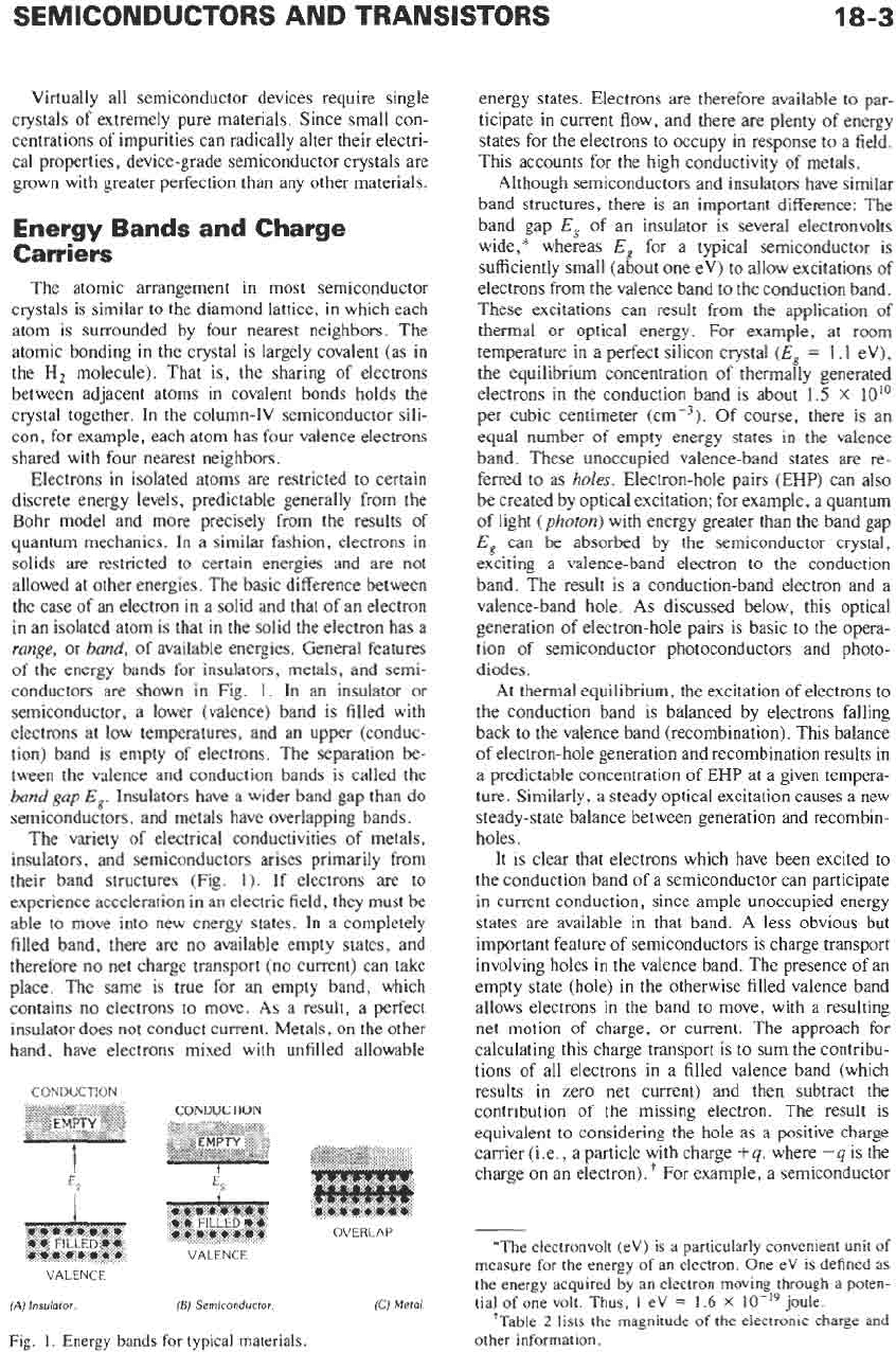
When impurities are introduced into an otherwise
perfect crystal, additional levels are created in the
energy-band structure, usually within the band gap. For
example, an impurity from column V of the periodic
table (phosphorus,
P;
arsenic, As; antimony,
Sb)
intro-
duces an energy level very near the conduction band in
germanium or silicon. This level is filled with electrons
at
0
K,
and very little thermal energy is required to
excite these electrons to the conduction band (Fig. 2A).
Thus at room temperature virtually all of the electrons
in the impurity level are “donated” to the conduction
band. Such an impurity level is called a
donor
level, and
the column-V impurities in germanium or silicon are
called donor impurities. Material doped with donor
impurities can have a considerable number of electrons
in the conduction band, even when the temperature
is
too low for the thermally generated
EHPs
to be appreci-
able. Thus for semiconductors doped with a significant
number of donor atoms, the electron concentration
n
will be much greater than the hole concentrationp. This
is n-type material.
Atoms from column
I11
(boron, B; aluminum, Al;
gallium, Ga; indium,
In)
introduce impurity levels in
germanium or silicon near the valence band (Fig.
2B).
These levels are empty of electrons at
0
K.
At higher
temperatures, enough thermal energy
is
available to
excite electrons from the valence band into the impurity
level, leaving behind holes in the valence band. Since
this type of impurity level “accepts” electrons from the
valence band, it is called an
acceptor
level, and the
column-111 impurities are acceptor impurities in germa-
**I*.
f‘flt
(A)
Electrons are
therrnolly
exclted
from
a
donor
leuel
to
the
conduction
band.
bond
(B)
Volence-band electrons
ore
excited
to E,, leaving
holes
in
the udence
Fig.
2.
Donor
and
acceptor
levels
(Ed
and
E,)
in
a
semicon-
ductor.
SEMICONDUCTORS
AND
TRANSISTORS
18-5
nium and silicon. Doping with acceptor impurities can
create a semiconductor with a hole density much greater
than the conduction-band electron density (p-type ma-
terial)
.
A
semiconductor without doping impurities is called
intrinsic material, and the intrinsic carrier concentra-
tion
ni
is the concentration of thermally generated
electron-hole pairs. In silicon, for example, the intrinsic
concentration
nj
is about
10"
at room tempera-
ture. If silicon is doped with
10"
antimony atoms/cm3,
the conduction electron concentration
n
increases from
10"
to lOI5 crK3, a change of five orders
of
magni-
tude. As a result, the resistivity of silicon changes from
about
2
X
lo5
ohm-cm to 5 ohm-cm with this doping.
When a semiconductor is doped n-type or p-type,
one type of carrier dominates. In the example given
above, the conduction-band electrons outnumber the
holes in the valence band by many orders of magnitude.
We refer to the small number of holes in n-type material
as minority carriers and the relatively large number of
conduction electrons as majority carriers. Similarly,
electrons are the minority carriers in p-type material
and holes are the majority carriers.
Carrier Concentrations
In calculating semiconductor electrical properties
and analyzing device behavior, it is often necessary to
know the concentration of charge carriers in the materi-
al. The majority-carrier concentration is usually obvi-
ous in heavily doped material, since one majority
carrier is obtained for each impurity atom. The concen-
tration of minority carriers is not obvious, however,
unless we consider details of the electron distribution in
the solid. An important result of semiconductor statis-
tics is that the electron-hole product np at equilibrium is
a constant for a given material at a given temperature,
whether the material
is
doped or not:
np
=
ni2
0%.
1)
where
n
and p are the equilibrium electron and hole
concentrations, respectively. Thus, if we know the
majority-carrier concentration (e.g., from the doping
density) we can find the minority-carrier concentration
from Eq.
1.
For
example, if a silicon sample
(n,
=
1.5
X
10"
is doped with
lo1'
donors/cm3, the
electron concentration is essentially 10" and the hole
concentration is only
2.25
X
lo5
cm-3 at room
temperature. It
is
interesting to note from Eq. 1 that as
the majority-carrier concentration increases, the minor-
ity-carrier concentration must decrease.
If
a semiconductor contains both donors and accep-
tors, the exact relationship among the electron, hole,
donor, and acceptor concentrations can be obtained by
considering the requirements for space-charge neutrali-
ty. If the material is to remain electrostatically neutral,
the sum of the positive charges (holes and ionized donor
atoms
Ndt)
must balance the sum
of
the negative
charges (electrons and ionized acceptor atoms
Na-):
If the material is strongly n-type (n
>>
p)
and all of the
impurities are ionized, we can approximate Eq.
2
by
n
EZ
Nd
-
No.
Drift of Carriers
The electrons and holes in a semiconductor are in
constant motion due to their thermal energy. At thermal
equilibrium, the movement is random, and carriers are
scattered from lattice atoms, impurities, and defects.
Since the scattering is completely random, there is no
net motion of the group of carriers over a period of
time. On the other hand, if an electric field is applied to
the sample, a net drift of carriers is superimposed on the
random thermal motion. Thus, a field
8,
applied in the
direction results in a net force
q8,
on each hole and
-qgX
on each electron. The current resulting from this
net drift is just the number of carriers crossing a given
area A per unit time (number of carriers times velocity)
multiplied by the charge of the carrier:
I
=
qApvp
-
qAn(-v,)
(Eq.
3)
In this equation,
vp
is the average drift velocity
of
holes
in the
n
direction, and
-v,
is the average electron
velocity, which is in the opposite direction. The result-
ing electrical conductivity is usually written in terms of
the mobility of each charge carrier. This quantity
measures the ease with which carriers drift in a given
material. The hole mobility
pp
is the average drift
velocity per unit applied field
vp/8,
and similarly for
electron mobility
p,.
Thus the current is
I
=
qA
(ppp
+
p,n)8
=
&A (Eq.
4)
where the conductivity of the sample
u
has the units
(ohm-cm)-'. Conductivity is determined by electron
and hole concentration
(n,
p),
and therefore by the
doping of the sample, and also by the carrier mo-
bilities.
If a semiconductor bar contains both types of carri-
ers, holes drift as a group in the direction of the electric
field, and electrons drift in the opposite direction. Both
components of current are in the direction
of
the
8
field, however, since conventional current is positive in
the direction of hole flow and opposite to the direction
of electron flow.
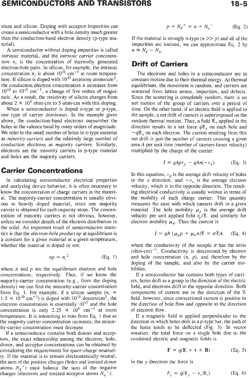
If a magnetic field is applied perpendicular
to
the
direction in which holes drift in a p-type bar, the path
of
the holes tends to be deflected (Fig.
3).
In vector
notation, the total force on a single hole due to the
combined electric and magnetic fields is
F
=
q(E
+
v
x
B)
(Eq.
5)
In the
y
direction the force is
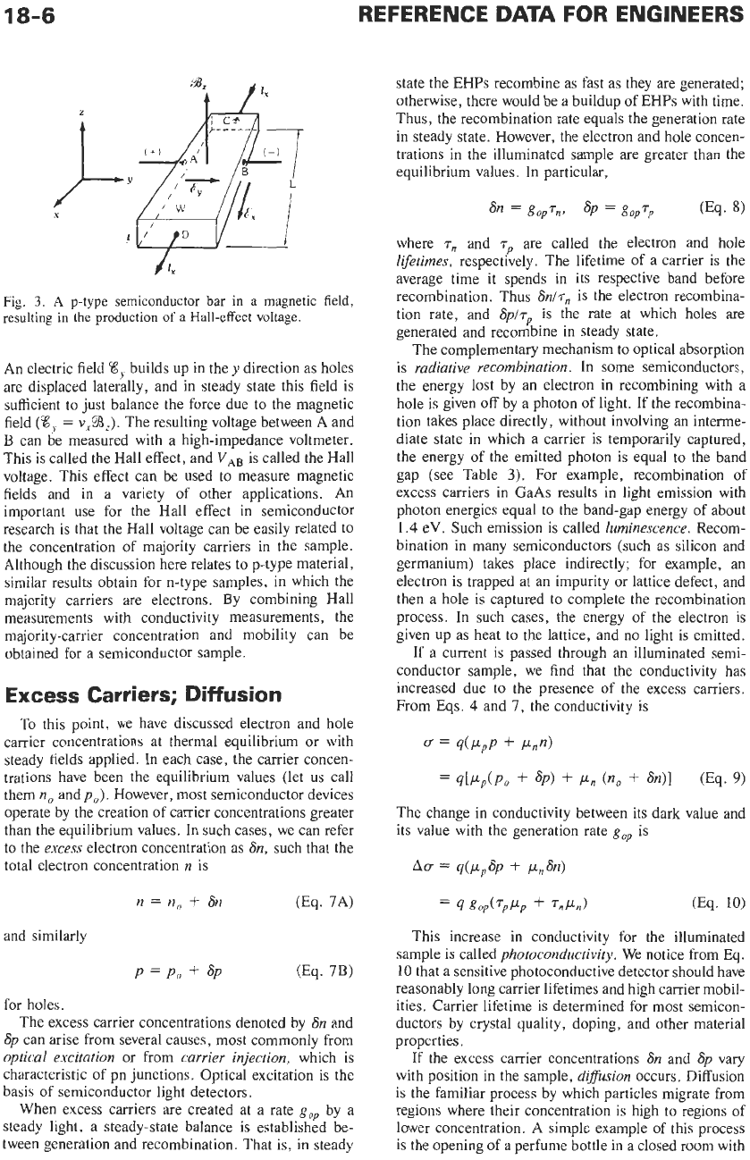
18-6
REFERENCE
DATA
FOR ENGINEERS
z
X
Fig.
3.
A
p-type
semiconductor
bar
in
a
magnetic field,
resulting
in
the production
of
a
Hall-effect voltage.
An electric field
8,
builds up in the
y
direction as holes
are displaced laterally, and in steady state this field is
sufficient to just balance the force due to the magnetic
field
(8,
=
~$3~).
The resulting voltage between A and
B
can be measured with a high-impedance voltmeter.
This is called the Hall effect, and
VAB
is called the Hall
voltage. This effect can be used to measure magnetic
fields and in a variety of other applications. An
important use for the Hall effect in semiconductor
research is that the Hall voltage can be easily related to
the concentration of majority carriers in the sample.
Although the discussion here relates to p-type material,
similar results obtain for n-type samples, in which the
majority carriers are electrons. By combining Hall
measurements with conductivity measurements, the
majority-carrier concentration and mobility can be
obtained for a semiconductor sample.
Excess
Carriers; Diffusion
To
this point, we have discussed electron and hole
carrier concentrations at thermal equilibrium
or
with
steady fields applied.
In
each case, the carrier concen-
trations have been the equilibrium values (let
us
call
them
no
and
po).
However, most semiconductor devices
operate by the creation of carrier concentrations greater
than the equilibrium values.
In
such cases, we can refer
to
the
excess
electron concentration as
Sn,
such that the
total electron concentration
n
is
n
=
no
+
Sn
(Eq. 7A)
and similarly
P=Po
+
SP
(Eq. 7J3)
for holes.
The excess carrier concentrations denoted by
Sn
and
Sp
can arise from several causes, most commonly from
optical excitation
or from
carrier injection,
which is
characteristic
of
pn junctions. Optical excitation is the
basis of semiconductor light detectors.
When excess carriers are created at a rate
g,
by a
steady light? a steady-state balance is established be-
tween generation and recombination. That is, in steady
state the EHPs recombine as fast as they are generated;
otherwise, there would be a buildup of EHPs with time.
Thus, the recombination rate equals the generation rate
in steady state. However, the electron and hole concen-
trations in the illuminated sample are greater than the
equilibrium values. In particular,
an
=
goprnn.
SP
=
goprp
0%.
8)
where
T-,,
and
rp
are called the electron and hole
lifetimes,
respectively. The lifetime of a carrier is the
average time it spends in its respective band before
recombination. Thus
Sn/T-,,
is the electron recombina-
tion rate, and
Sp/rp
is the rate at which holes are
generated and recombine in steady state.
The complementary mechanism to optical absorption
is
radiative recombination.
In
some semiconductors,
the energy lost by an electron in recombining with a
hole
is
given off by a photon
of
light.
If
the recombina-
tion takes place directly, without involving an interme-
diate state in which a carrier is temporarily captured,
the energy
of
the emitted photon is equal
to
the band
gap (see Table
3).
For example, recombination of
excess carriers in GaAs results in light emission with
photon energies equal to the band-gap energy of about
1.4
eV. Such emission
is
called
luminescence.
Recom-
bination in many semiconductors (such as silicon and
germanium) takes place indirectly; for example, an
electron is trapped at an impurity or lattice defect, and
then a hole is captured to complete the recombination
process. In such cases, the energy of the electron is
given up as heat to the lattice, and no light is emitted.
If
a current is passed through an illuminated semi-
conductor sample, we find that the conductivity has
increased due to the presence of the excess carriers.
From
Eqs.
4
and
7,
the conductivity
is
=
dPpP
+
&In)
=
dPp(Po
+
SP)
+
Pn
(no
+
841
(Eq.
9)
The change in conductivity between its dark value and
its value with the generation rate
g,
is
Af7
=
dPp%J
+
PnSn)
(Eq.
10)
This increase in conductivity for the illuminated
sample is called
photoconductivity.
We notice from Eq.
10
that a sensitive photoconductive detector should have
reasonably long carrier lifetimes and high carrier mobil-
ities. Carrier lifetime is determined for most semicon-
ductors by crystal quality, doping, and other material
properties.
If the excess carrier concentrations
Sn
and
Sp
vary
with position in the sample,
drfision
occurs. Diffusion
is the familiar process by which particles migrate from
regions where their concentration is high to regions of
lower concentration.
A
simple example of this process
is the opening of a perfume bottle in a closed room with
-
-
9
gop(7pP.p
+
TnPn)
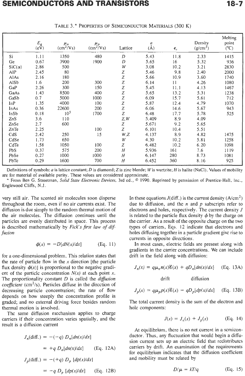
18-7
TABLE 3.
*
PROPERTIES
OF
SEMICONDUCTOR MATERIALS (300
K)
Si
Ge
Sic(&)
AIP
AlAs
AlSb
GaP
GaAs
GaSb
InP
InAs
InSb
ZnS
ZnSe
ZnTe
CdS
CdSe
CdTe
PbS
PbSe
PbTe
E,
(eV)
1.11
0.67
2.86
2.45
2.16
1.6
2.26
1.43
0.7
1.35
0.36
0.18
3.6
2.7
2.25
2.42
1.73
1.58
0.37
0.27
0.29
Pn
PP
(cm2/Vs) (cm2/Vs) Lattice
1350 480
D
3900 1900
D
500
W
80 Z
180
Z
200 300 Z
300 150 Z
8500 400 Z
5000
1000 Z
4000 100
Z
22600 200 Z
105 1700 Z
110
z,
w
600 Z
100
Z
250 15
w,z
650
W
1050 100
Z
575 200
H
1000 1000
H
1600 700
H
a
(A)
5.43
5.65
3.08
5.46
5.66
6.14
5.45
5.65
6.09
5.87
6.06
6.48
5.409
5.671
6.101
4.137
4.30
6.482
5.936
6.147
6.452
E,
11.8
16
10.2
9.8
10.9
11
11.1
13.2
15.7
12.4
14.6
17.7
8.9
9.2
10.4
8.9
10.2
10.2
161
280
360
Density
(g/cm3)
2.33
5.32
3.21
2.40
3.60
4.26
4.13
5.31
5.61
4.79
5.67
5.78
4.09
5.65
5.51
4.82
5.81
6.20
7.6
8.73
8.16
Melting
point
("C)
1415
936
2830
2000
1740
1080
1467
1238
712
1070
943
525
1475
1258
1098
1119
1081
925
Definitions
of
symbols:
a
is
lattice constant;
D
is diamond; Z is zinc blende;
W
is wurtzite;
H
is halite (NaC1). Values
of
mobility
*
From
Ben
G. Streetman,
Solid
State
Electronic
Devices,
3rd ed.,
0
1990. Reprinted by permission
of
Prentice-Hall, Inc.,
are
for
material
of
available purity. These values are considered approximate.
Englewood Cliffs,
N.J.
very still air. The scented air molecules soon disperse
throughout the room, even if no air currents exist. The
diffusion is due simply to the random thermal motion
of
the air molecules. The diffusion continues until the
particles are evenly distributed in space. This process
is described mathematically by
Fick's
first
law
of
dg-
fusion
&x)
=
-D[dN(x)/dU]
(Eq.
11)
for a one-dimensional problem. This relation states that
the rate of particle flow in the
x
direction [the particle
flux density
+(x)]
is proportional to the negative gradi-
ent of the particle concentration
N(x)
at each point
x.
The proportionality constant
D
is called the
difision
coeficient
(cm2/s). Particles diffuse in the direction of
decreasing particle concentration; the rate of flow
depends on how steeply the concentration profile
is
graded; and no external driving force besides random
thermal motion is involved.
The same diffusion mechanism applies to charge
carriers if their concentration varies spatially, and the
result is a diffusion current
J,(diff.)
=
-(-q)
D,[dn(x)/dx]
=
+q
D,[dn(xj/dU]
(Eq.
12A)
J,(diff.)
=
-(+q)
D,
[dp(x)ldw]
=
-9
D,
[dp(x)/dx]
(Eq. 12B)
In
these equations J(diff.) is the current density (A/cm2)
due to diffusion, and the
n
and
p
subscripts refer to
electrons and holes, respectively. The current density
J
is related to the particle flux density
4
by the charge on
the carrier. As a result of the opposite charge on the two
types of carriers, Eqs. 12 indicate that electrons and
holes diffusing together in a particle gradient give rise to
currents in opposite directions.
In most cases, electric fields are present along with
gradients in the carrier concentrations. We can include
drift in the field along with diffusion:
J,(x)
=
qp,n(x)%(x)
+
qD,[dn(x)/dx]
(Eq. 13A)
drift diffusion
J,O
=
qp,p(x)W)
-
qD,[dp(x)/dxI
0%.
13B)
The total current density is the sum of the electron and
hole components:
J(x)
=
J&)
+
JJ.4
(Eq.
14)
At equilibrium, there is no net current in a semicon-
ductor. Thus, any fluctuation that would begin a diffu-
sion current sets up an electric field that redistributes
carriers by drift. An examination
of
the requirements
for equilibrium indicates that the diffusion coefficient
and mobility must be related by
Dlp
=
kT/q
(Eq.
15)