Middleton W.M. (ed.) Reference Data for Engineers: Radio, Electronics, Computer and Communications
Подождите немного. Документ загружается.

18-8
REFERENCE
DATA
FOR ENGINEERS
for either carrier type. This important equation is called
the
Einstein relation.
It allows
us
to measure either
D
or
p
and calculate the other.
In many carrier-diffusion problems, a steady-state
distribution is maintained by a constant generation of
excess carriers at some point in the semiconductor. For
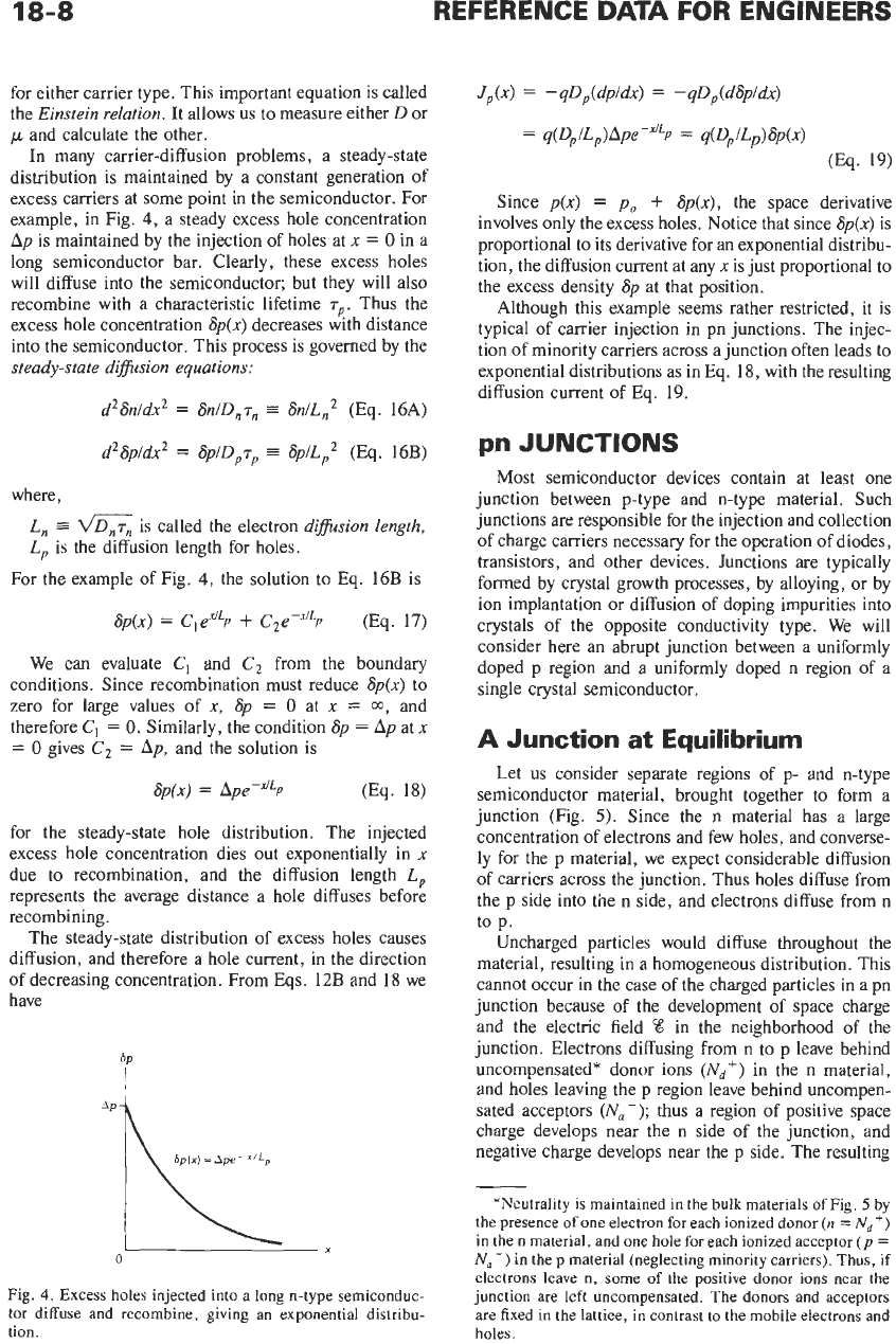
example, in Fig.
4,
a steady excess hole concentration
Ap
is
maintained by the injection of holes at
x
=
0
in a
long semiconductor bar. Clearly, these excess holes
will diffuse into the semiconductor; but they will also
recombine with a characteristic lifetime
7,.
Thus the
excess hole concentration
Sp(x)
decreases with distance
into the semiconductor. This process is governed by the
steady-state difision equations:
d2Sn/dx2
=
Sn/D,r,,
=
6n/Ln2
(Eq. 16A)
d2Spldx2
=
Sp/Dprp
=
Sp/Lp2
(Eq. 16B)
where,
L,
L,
is the diffusion length for holes.
is called the electron
difision
length,
For the example of Fig.
4,
the solution to Eq. 16B is
We can evaluate
C1
and
C2
from the boundary
conditions. Since recombination must reduce
Sp(x)
to
zero for large values of
x,
Sp
=
0
at
x
=
m,
and
therefore
C1
=
0.
Similarly, the condition
Sp
=
Ap
at
x
=
0
gives
C2
=
Ap,
and the solution is
Sp(x)
=
Ape-dLp
(Eq. 18)
for the steady-state hole distribution. The injected
excess hole concentration dies out exponentially in
x
due to recombination, and the diffusion length
L,
represents the average distance a hole diffuses before
recombining.
The steady-state distribution of excess holes causes
diffusion, and therefore a hole current, in the direction
of decreasing concentration. From Eqs
.
12B and
18
we
have
Fig.
4.
Excess holes injected into a long n-type semiconduc-
tor diffuse and recombine, giving an exponential distribu-
tion.
J,(x)
=
-qD,(dp/dx)
=
-qDP(d8p/dx)
=
q(D,/L,)Ape-X/LP
=
q(D,/Lp)Sp(x)
(Eq. 19)
Since
p(x)
=
po
+
Sp(x),
the space derivative
involves only the excess holes. Notice that since
Sp(x)
is
proportional to its derivative for an exponential distribu-
tion, the diffusion current at any
x
is just proportional to
the excess density
Sp
at that position.
Although this example seems rather restricted, it is
typical of carrier injection in pn junctions. The injec-
tion of minority carriers across a junction often leads to
exponential distributions as in Eq. 18, with the resulting
diffusion current
of
Eq. 19.
pn
JUNCTIONS
Most semiconductor devices contain at least one
junction between p-type and n-type material. Such
junctions are responsible for the injection and collection
of charge carriers necessary for the operation of diodes,
transistors, and other devices. Junctions are typically
formed by crystal growth processes, by alloying, or by
ion implantation or diffusion
of
doping impurities into
crystals
of
the opposite conductivity type. We will
consider here an abrupt junction between a uniformly
doped p region and a uniformly doped n region of a
single crystal semiconductor.
A
Junction at Equilibrium
Let us consider separate regions
of
p- and n-type
semiconductor material, brought together to form a
junction (Fig.
5).
Since the n material has a large
concentration of electrons and few holes, and converse-
ly for the p material, we expect considerable diffusion
of carriers across the junction. Thus holes diffuse from
the p side into the n side, and electrons diffuse from n
to p.
Uncharged particles would diffuse throughout the
material, resulting in a homogeneous distribution. This
cannot occur in the case of the charged particles in a pn
junction because of the development of space charge
and the electric field
%
in the neighborhood of the
junction. Electrons diffusing from n to p leave behind
uncompensated* donor ions
(Ndt)
in
the
n
material,
and holes leaving the p region leave behind uncompen-
sated acceptors
(Na-);
thus a region of positive space
charge develops near the n side
of
the junction, and
negative charge develops near the p side. The resulting
*Neutrality is maintained in the bulk materials of Fig.
5
by
the presence of
one
electron for each ionized donor
(n
=
Nd+)
in the
n
material, and one
hole for
each ionized acceptor
(p
=
Na-)
in
the p material (neglecting minority carriers).
Thus,
if
electrons leave
n,
some of the positive donor ions near the
junction are left uncompensated.
The
donors
and
acceptors
are fixed in
the
lattice, in contrast to the mobile electrons and
holes.
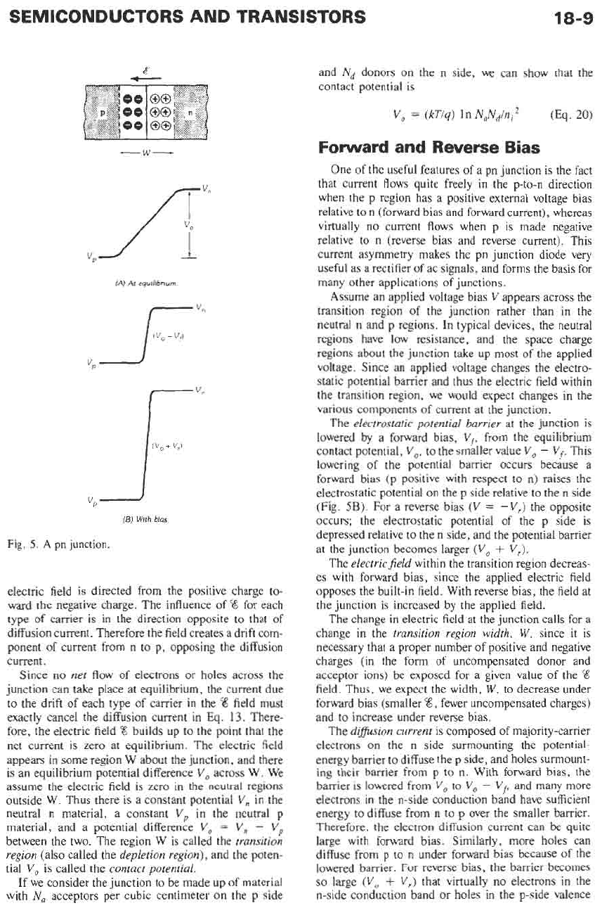
SEMICONDUCTORS AND TRANSISTORS
18-9
G
-W-
(A)
At
equilibrium
(E)
Wlth
bias
Fig.
5.
A
pn
junction.
electric field is directed from the positive charge to-
ward the negative charge. The influence of
%
for each
type of carrier is in the direction opposite to that of
diffusion current. Therefore the field creates a drift com-
ponent of current from
n
to p, opposing the diffusion
current.
Since
no
net
flow of electrons or holes across the
junction can take place at equilibrium, the current due
to
the drift
of
each type of carrier in the
%
field must
exactly cancel the diffusion current in Eq.
13.
There-
fore, the electric field
%
builds up to the point that the
net current is zero at equilibrium. The electric field
appears
in
some region
W
about the junction, and there
is an equilibrium potentia1 difference
V,
across W. We
assume the electric field is zero in the neutral regions
outside
W.
Thus there is a constant potential
V,
in the
neutral
n
material, a constant
V,
in the neutral p
material, and a potential difference
V,
=
V,
-
Vp
between the two. The region W is called the
transition
region
(also called the
depletion region),
and the poten-
tial
V,
is called the
contact potential.
If we consider the junction
to
be made up of material
with
N,
acceptors per cubic centimeter
on
the p side
and
Nd
donors
on
the n side, we can show that the
contact potential is
V,
=
(kTlq)
In
N,NdIni2
(Eq.
20)
Forward and Reverse Bias
One of the useful features of a pn junction is the fact
that current flows quite freely in the p-to-n direction
when the p region has a positive external voltage bias
relative to n (forward bias and forward current), whereas
virtually
no
current flows when
p
is made negative
relative to
n
(reverse bias and reverse current). This
current asymmetry makes the pn junction diode very
useful as a rectifier of ac signals, and forms the basis for
many other applications of junctions.
Assume an applied voltage bias
V
appears across the
transition region of the junction rather than
in
the
neutral
n
and p regions.
In
typical devices, the neutral
regions have low resistance, and the space charge
regions about the junction take up most of the applied
voltage. Since an applied voltage changes the electro-
static potential barrier and thus the electric field within
the transition region, we would expect changes in the
various components of current at the junction.
The
electrostatic potential barrier
at the junction
is
lowered by a forward bias,
Vp
from the equilibrium
contact potential,
V,,
to the smaller value
V,
-
Vf.
This
lowering of the potential barrier occurs because a
forward bias (p positive with respect to
n)
raises the
electrostatic potential on the p side relative to the
n
side
(Fig.
5B).
For a reverse bias
(V
=
-Vr)
the opposite
occurs; the electrostatic potential of the p side is
depressed relative to the
n
side, and the potential barrier
at the junction becomes larger
(V,
+
Vr).
The
electric field
within the transition region decreas-
es with forward bias, since the applied electric field
opposes the built-in field. With reverse bias, the field at
the junction is increased by the applied field.
The change in electric field at the junction calls for a
change in the
transition region width,
W,
since it is
necessary that a proper number of positive and negative
charges (in the form of uncompensated donor and
acceptor ions) be exposed for a given value of the
%
field. Thus, we expect the width,
W,
to decrease under
forward bias (smaller
%
,
fewer uncompensated charges)
and
to
increase under reverse bias.
The dzfision
current
is composed of majority-carrier
electrons
on
the
n
side surmounting the potential-
energy barrier to diffuse the p side, and holes surmount-
ing their barrier
from
p to
n.
With forward bias, the
barrier is lowered from
V,
to
V,
-
Vp
and many more
electrons in the n-side conduction band have sufficient
energy to diffuse from
n
to p over the smaller barrier.
Therefore, the electron diffusion current can be quite
large with forward bias. Similarly, more holes can
diffuse from p to n under forward bias because of the
lowered barrier. For reverse bias, the barrier becomes
so
large
(V,
+
V,)
that virtually no electrons in the
n-side conduction band or holes
in
the p-side valence
18-10
REFERENCE
DATA
FOR ENGINEERS
band have enough energy to surmount it. Therefore, the
diffusion current is usually negligible for reverse bias.
The
drift current
is relatively insensitive to the height
of the potential barrier. The reason for this is that the
drift current is limited
not
by
howfast
carriers are swept
down the barrier,
but
rather
how often.
For example,
minority-carrier electrons on the p side which wander
into the transition region will be swept down the barrier
by the
8
field, giving rise to the electron component of
drift current. However, this current is small not because
of the size of the barrier, but because there are very few
minority electrons in the p side to participate. Every
p-side electron that diffuses to the transition region will
be swept down the potential energy hill, whether the hill
is large or small. Similar comments apply regarding the
drift of minority holes from the n side to the p side of
the junction. To a good approximation, therefore, the
electron and hole drift currents at the junction are
independent of the applied voltage.
The supply of minority carriers on each side of the
junction required to participate in the drift component
of current is generated by thermal excitation of elec-
tron-hole-pairs (ENPs). For example, an EHP created
near the junction on the p side provides a minority
electron in the p material. If the EHP is generated
within a diffusion length
L,
of the transition region, this
electron can diffuse
to
the junction and be swept down
the barrier to the
n
side. The resulting current
is
commonly called the
generation current
since its mag-
nitude depends entirely upon the rate of generation of
EHP. This generation current can be greatly increased
by optical excitation
of
EHPs near the junction (the pn
junction
photodiode).
The
total
current
crossing the junction is composed
of the sum of the diffusion and drift components. The
electron and hole diffusion currents are both directed
from
p
to n (although the particle flow directions are
opposite to each other), and the drift currents are from
n
to p. The
net
current crossing the junction is zero at
equilibrium, since the drift and diffusion components
cancel for each type of carrier. Under reverse bias, both
diffusion components are negligible because of the large
barrier at the junction, and the only current is the
relatively small (and essentially voltage-independent)
generation current from
n
to p.
We expect from Fig.
4
that injection of excess holes
from p
to
n
will produce a
distribution
of excess holes in
the
n
material. As the holes diffuse deeper into the n
region, they recombine with electrons. and the resulting
excess hole distribution is obtained
as
a
solution
of
the
diffusion equation, Eq.
16B.
If
the
n
region is long
compared with the hole diffusion length,
L,,
the
solution is exponential, as in Fig.
4.
Similarly, the
injected electrons in the p material diffuse and recom-
bine, giving an exponential distribution of excess elec-
trons. These excess carrier distributions must be ac-
counted for in switching a pn junction from forward bias
to reverse bias.
By
evaluating the diffusion currents of electrons and
holes across the junction, it can be shown that the
current-voltage characteristic of the diode is given by
Equation 21 is called the
diode equation,
which
describes the total current through the diode for either
forward or reverse bias. We can calculate the current
with reverse bias (commonly called the reverse satura-
tion current) by letting
V
=
-V,
I
=
qA[(D,/L,)p,,
+
(D,/L,)n,](e-4Vr’kr
-
1)
(Eq.
22)
If
V,
is larger than a few
kT/q,
the total current is just
the reverse saturation current
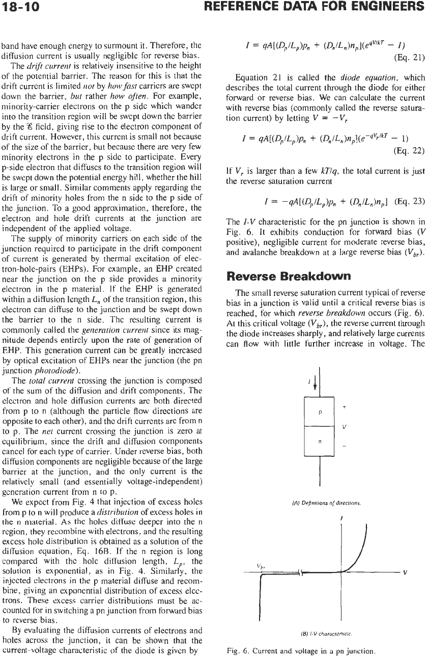
The
I-V
characteristic for the pn junction is shown in
Fig.
6.
It exhibits conduction for forward bias
(V
positive), negligible current for moderate reverse bias,
and avalanche breakdown at a large reverse bias
(Vbr).
Reverse Breakdown
The small reverse saturation current typical of reverse
bias in a junction is valid until a critical reverse bias is
reached, for which
reverse breakdown
occurs (Fig.
6).
At this critical voltage
(Vbr),
the reverse current through
the diode increases sharply, and relatively large currents
can flow with little further increase in voltage. The
(A)
Definitions
of
directions
I
(E)
I-V
choracterlstic.
Fig.
6.
Current
and
voltage
in
a
pn
junction.
18-11
existence of a critical breakdown voltage introduces
almost a right-angle appearance to the reverse charac-
diodes.
There
is
nothing inherently destructive about reverse
breakdown. If the current is limited to a reasonable
value by the external circuit, the pn junction can be
operated safely in the reverse-breakdown condition.
Useful devices called
breakdown
diodes
are designed to
operate in the reverse-breakdown regime of their
characteristics.
Reverse breakdown can occur by two mechanisms,
each of which requires a critical electric field in the
junction transition region. The first mechanism, called
the
zener
effect,
is operative at low voltages (up to a few
volts reverse bias). If the breakdown occurs at higher
voltages (from a few volts to hundreds of volts), the
mechanism is
avalanche breakdown.
Zener breakdown occurs in heavily doped junctions
in which the transition from the p side to the n side is
very abrupt. Under these conditions, the potential
barrier separating carriers on the two sides of the
junction
is
very narrow, and a quantum-mechanical
process called
tunneling
can take place. In effect,
electrons from the p-side valence band are able to
tunnel across the barrier into the empty states in the
n-side conduction band when a small reverse bias is
applied. The result is a strong current from n to p in the
diode, causing zener breakdown. We shall discuss
tunneling again in relation to tunnel diodes in a later
section.
For diodes with lighter doping or with a graded
junction, the avalanche mechanism is the operative
breakdown process. In this effect, the electric field in
the transition region becomes strong enough under
reverse bias to accelerate carriers to quite high kinetic
energy. For example, if a minority hole is generated
thermally on the n side and wanders into the transition
region, it is swept by the junction field to the p side. If
the field is high enough, the hole can collide with the
lattice with sufficient energy to create an electron-hole
pair.
As
a result, the newly created hole is swept to the p
side and the electron
is
swept to the n side. With one
carrier entering the transition region, we in effect have
three carriers leaving. This
carrier multiplication
adds
to the reverse current. Furthermore, if on the average
each carrier (including carriers created by ionizing
collisions) can create one
EHP
during its transit across
the transition region, a runaway (avalanche) process
develops. Avalanche breakdown usually occurs at a
sharply
defined breakdown voltage which corresponds
to the establishment of a critical field in the transition
region. This critical field is that necessary to cause a
series
of
ionizing collisions by carriers in transit across
the transition region.
Capacitance and Transient
Behavior
Since many pn-junction devices are used in ac
circuits or for switching applications, it is important to
consider their time-dependent properties. The transient
behavior of a junction is influenced strongly by the
presence of stored charge. For example, the charge
(Q)
due to excess minority carriers in a forward-biased
junction must be changed as the current varies. Since
this charge cannot be altered instantaneously, current
and voltage may vary in a complex fashion for the
transient case.
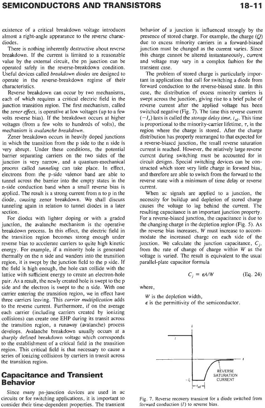
The problem of stored charge is particularly impor-
tant in applications that call for switching a diode from
forward conduction to the reverse-biased state. In this
case, the distribution of excess minority carriers is
swept across the junction, giving rise to a brief pulse of
reverse current after the applied voltage has been
switched negative (Fig.
7).
The time this reverse current
(
-Zr)
lasts is called the
storage
deZay
time,
tsd.
This time
is proportional to the minority-carrier lifetime,
T,
in the
region where the charge is stored. After the charge
distribution has properly rearranged to that expected for
a reverse-biased junction, the small reverse saturation
current is reached. However, the relatively large reverse
current during switching must be accounted for in
circuit designs. Special switching devices can be con-
structed which store very little charge in forward bias,
and therefore are able to switch from the forward to the
reverse state with a minimum of time delay or reverse
current.
When ac signals are applied to a junction, the
necessity for buildup and depletion of stored charge
causes the voltage to lag behind the current. The
resulting capacitance is an important junction property.
For a reverse-biased junction, the capacitance is due to
the changing charge in the depletion region (Fig.
5).
As
the reverse bias increases,
W
must increase to accom-
modate the increased charge on each side of the
junction. We calculate the junction capacitance,
Cj,
from the rate of change of charge within
W
as the
voltage is varied. The result is equivalent to the usual
parallel-plate capacitor formula
ci
=
€A/w
(Eq.
24)
where,
W
is the depletion width,
E
is the permittivity of the semiconductor.
i
I,+
CURRENT
kf5d-I
Fig.
7.
Reverse
recovery transient for a
diode
switched from
forward
conduction
(I)
to reverse bias.
18-12
REFERENCE
DATA
FOR ENGINEERS
Since
W
depends
on
the reverse bias,
Cj
is a
voltage-
variable capacitance.
This property can be used in
tuning circuits, as discussed below.
For forward bias, ac variations impressed
on
a steady
forward current
I
(dc) call for variations in stored charge
of the minority carrier distribution (Fig.
4).
A
forward-
biased pn diode in which hole injection dominates
responds
to
ac signals with an equivalent
RC
time
constant
rp
required for redistribution
of
the charge due
to holes stored in the
n
region. The current in a
forward-biased junction
(V
>>
kT/q)
is
=
I
eqVikT
(E¶.
25)
where
I,
is the magnitude of the saturation current,
described in Eq.
23.
If we take the derivative with respect to V, we find the
ac conductance to be
G,,
=
(q/kT)
I,
eqVikT
=
(q/kT)
I
(Eq.
26)
Thus charge-storage capacitance
C,
=
rPG
is
C,
=
(q
rp/k7J
I
In
summary, the reverse-bias junction capacitance,
Cj,
varies with the reverse bias voltage,
V,,
and the
forward bias capacitance,
C,,
varies with the forward
bias current,
I.
The storage delay time is an important
limitation in switching circuits, and the forward-bias
capacitance is important in high-frequency ac circuits.
In
either case, the effects of charge storage can be
minimized by reducing the carrier lifetime in the
minority-carrier storage region. One approach used in
silicon devices involves doping the junction with gold,
which introduces a high density of recombination
centers, thereby reducing carrier lifetime.
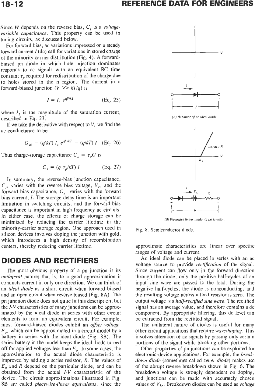
DIODES
AND
RECTIFIERS
The most obvious property of a pn junction is its
unilateral
nature; that is, to a good approximation it
conducts current in only one direction. We can think of
an
ideal diode
as a short circuit when forward biased
and an open circuit when reverse biased (Fig.
8A).
The
pn
junction diode does not quite fit this description, but
the
I-V
characteristics of many junctions can be approx-
imated by the ideal diode in series with other circuit
elements to form an equivalent circuit. For example,
most forward-biased diodes exhibit an
offset
voltage,
E,,
which can be approximated in a circuit model by a
battery in series with the ideal diode (Fig.
8B).
The
series battery in the model keeps the ideal diode turned
off
for applied voltages less than
Eo.
In
some cases, the
approximation to the actual diode characteristic is
improved by adding a series resistor,
R.
The values of
Eo
and
R
depend
on
the particular diode, and can be
obtained from the actual
I-V
characteristic of the
device. The circuit approximations illustrated in Fig.
8B are called
piecewise-linear equivalents,
since the
I
I
---c
-
++v--i-
(A)
Behouior
of
an
ldeol diode
I
(B]
Piecewise linear model
oipn
junction
Fig.
8.
Semiconductor diode.
approximate characteristics are linear over specific
ranges of voltage and current.
An
ideal diode can be placed in series with an ac
voltage source to provide
rectiJcation
of the signal.
Since current can flow only in the forward direction
through the diode, only the positive half-cycles of an
input sine wave are passed to the load. During the
negative half-cycles, the diode is nonconducting, and
the resulting voltage across a load resistor is zero. The
output voltage is a
half-rectiJied sine wave.
The rectified
signal has an average value, and therefore contains a
dc
component. By appropriate filtering, this dc level can
be extracted from the rectified signal.
The unilateral nature of diodes is useful for many
other circuit applications that require
waveshaping.
This
involves alteration of ac signals by passing only certain
portions of the signal while blocking other portions.
Other properties of pn junctions can be exploited for
electronic-device applications. For example, the
break-
down diode
(sometimes called
zener diode)
makes use
of the abrupt reverse breakdown shown in Fig.
6.
The
breakdown voltage is strongly dependent
on
doping,
and junctions can be made with accurately chosen
values of
Vb,.
Breakdown diodes can be used as
voltage
18-13
regulators in circuits with varying inputs. Such a device
can also be used as a
reference diode:
since the
breakdown voltage of a particular diode is known, the
voltage across it during breakdown can be used as a
reference in circuits that require a known value of
voltage.
The junction capacitance described by Eq.
24
can be
put to use in a device called a
varactor.
Since
Cj
is
inversely proportional to the depletion width,
W,
and
W
varies with the reverse bias,
V,,
the junction is a
voltage-variable capacitor.
For an abrupt junction,
C,
is
proportional to Thus it
is
possible to vary
Cj
by
choosing values of the applied bias. A set
of
varactors
can be used, for example, to replace variable-plate
capacitors in the tuning section of a radio receiver. By
proper adjustment of doping profiles in the junction, the
voltage dependence of
Cj
can be tailored for the specific
application.
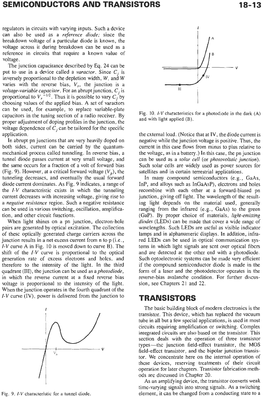
In abrupt pn junctions that are very heavily doped on
both sides, current can be carried by the quantum-
mechanical process called tunneling.
In
reverse bias, a
tunnel diode passes current at very small voltage, and
the same occurs for a fraction of a volt of forward bias
(Fig.
9).
However, at a critical forward voltage
(V,),
the
tunneling decreases, and eventually the usual forward
diode current dominates. As Fig.
9
indicates, a range of
the
I-V
characteristic exists in which the tunneling
current decreases with increasing voltage, giving rise to
a
negative resistance
region. Such a negative resistance
can be used in various switching, oscillation, amplifica-
tion, and other circuit functions.
When light shines
on
a pn junction, electron-hole
pairs are generated by optical excitation. The collection
of these optically generated charge carriers across the
junction results in a net excess current from n to p (i.e.,
I-V
curve
A
in Fig.
10
is moved down to curve B). The
shift of the
I-V
curve is proportional to the optical
generation rate of excess electrons and holes, and
therefore to the intensity of the light.
In
the third
quadrant
(111),
the junction can be used as
aphotodiode,
in which the reverse current at a fixed reverse bias
voltage is proportional to the intensity of the light.
When the junction operates in the fourth quadrant of the
I-V
curve
(IV),
power is delivered from the junction
to
I
I
I
Fig.
9.
I-V
characteristic for
a
tunnel
diode.
I
V
Ill
Fig.
10.
I-V
characteristics for
a
photodiode
in
the
dark
(A)
and
with
light
applied
(B).
the external load. (Notice that at
IV,
the diode current is
negative while the junction voltage
is
positive. Thus, the
current in this case flows from minus to plus relative to
the voltage, as in
a
battery.) In this case, the pn junction
can be used as a
solar cell
(or
photovoltaic junction).
Such solar cells are widely used as power sources for
satellites and in certain terrestrial applications.
In
many compound semiconductors (e.g., GaAs,
InP, and alloys such as InGaAsP), electrons and holes
recombine with each other at a forward-biased pn
junction, giving off light. The wavelength of the result-
ing light depends on the material used, generally
ranging from the infrared (e.g., GaAs) to the green
(Gap). By proper choice of materials,
light-emitting
diodes
(LEDs)
can be made that cover a wide range of
wavelengths. Such
LEDs
are useful as visible indicator
lamps and in alphanumeric displays.
In
addition, infra-
red
LEDs
can be used in optical communication sys-
tems in which light signals are sent over optical fibers
and are detected at the other end with a photodiode.
Such optoelectronic systems can be made very efficient
if the compound semiconductor diode is made in the
form
of
a laser and the photodetector operates in the
reverse-bias avalanche condition. For further discus-
sion, see Chapters
21
and
22.
TRANSISTORS
The basic building block
of
modern electronics is the
transistor. This device, which has replaced the vacuum
tube in all but a few special applications, is used in most
circuits requiring amplification or switching. Complex
integrated circuits are also based
on
the transistor. This
section deals with the operation of three transistor
types-the junction field-effect transistor, the
MOS
field-effect transistor, and the bipolar junction transis-
tor. We concentrate here on the internal operation
of
these devices, reserving treatments of their circuit
operation for later chapters. Transistor fabrication meth-
ods are discussed in Chapter
20.
As an amplifying device, the transistor converts weak
time-varying signals into strong signals. As a switching
element, it can be changed from a conducting state to a
18-14
REFERENCE
DATA
FOR ENGINEERS
nonconducting state quickly with the application
of
very little control power. In the field-effect transistor,
current through two terminals is varied by voltage
applied
to
a third terminal. In the bipolar transistor, the
current through two terminals is controlled by a small
current applied to a third terminal.
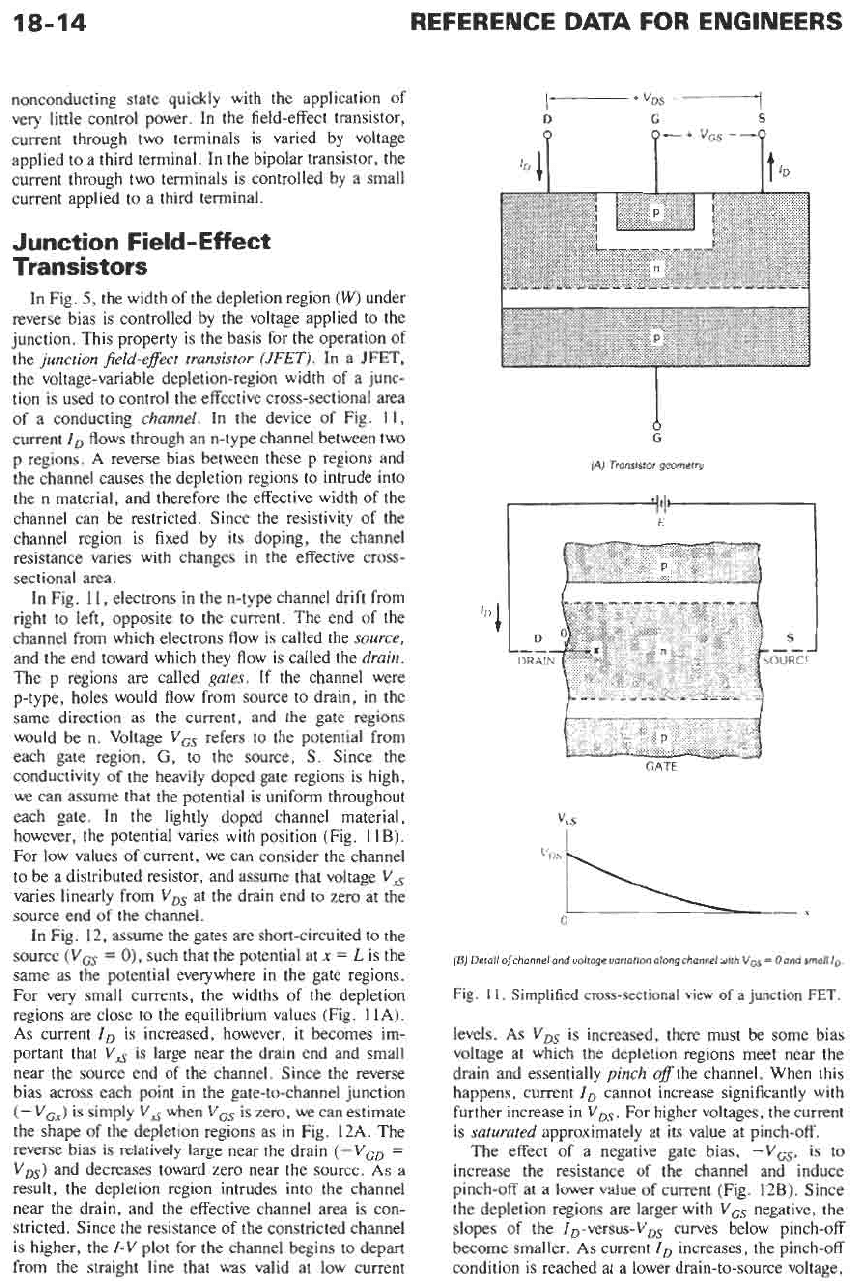
Junction Field-Effect
Transistors
In Fig.
5,
the width of the depletion region
(W)
under
reverse bias is controlled by the voltage applied
to
the
junction. This property is the basis for the operation of
the
junction jield-effect transistor
(JFET).
In a JFET,
the voltage-variable depletion-region width of a junc-
tion is used
to
control the effective cross-sectional area
of a conducting
channel.
In the device of Fig.
11,
current
I,
flows through an n-type channel between two
p regions.
A
reverse bias between these p regions and
the channel causes the depletion regions
to
intrude into
the n material, and therefore the effective width of the
channel can be restricted. Since the resistivity
of
the
channel region is fixed by its doping, the channel
resistance varies with changes in the effective cross-
sectional area.
In Fig.
11,
electrons in the n-type channel drift from
right
to
left, opposite to the current. The end
of
the
channel from which electrons flow is called the
source,
and the end toward which they flow is called the
drain.
The p regions are called
gates.
If the channel were
p-type, holes would flow from source to drain, in the
same direction
as
the current, and the gate regions
would be
n.
Voltage
VGs
refers to the potential from
each gate region,
G,
to the source,
S.
Since the
conductivity of the heavily doped gate regions is high,
we can assume that the potential is uniform throughout
each gate.
In the lightly doped channel material,
however, the potential varies with position (Fig.
11B).
For low values of current, we can consider the channel
to
be a distributed resistor, and assume that voltage
V,
varies linearly from
V,,
at the drain end to zero at the
source end of the channel.
In Fig.
12,
assume the gates are short-circuited to the
source
(V,
=
0),
such that the potential at
x
=
L
is the
same as the potential everywhere in the gate regions.
For very small currents, the widths of the depletion
regions are close to the equilibrium values (Fig.
11A).
As
current
ID
is
increased, however, it becomes im-
portant that
V,
is large near the drain end and small
near the source end of the channel. Since the reverse
bias across each point in the gate-to-channel junction
(-
V,)
is simply
V,
when
VGs
is
zero, we can estimate
the shape
of
the depletion regions as in Fig.
12A.
The
reverse bias is relatively large near the drain
(-VG,
=
VDs)
and decreases toward zero near the source.
As
a
result, the depletion region intrudes into the channel
near the drain, and the effective channel area is con-
stricted. Since the resistance
of
the constricted channel
is higher, the
I-V
plot for the channel begins to depart
from the straight line that was valid at low current
(A)
Translstor geometry
1-1
E
GATE
(BJ
Detallofchonnelandooltageuor~ofion
olongchannel
with
VGS
=
OandsrnolllD
Fig.
11.
Simplified
cross-sectional
view
of
a
junction
FET.
levels.
As
VDs
is increased, there must be some bias
voltage at which the depletion regions meet near the
drain and essentially
pinch off
the channel. When this
happens, current
I,
cannot increase significantly with
further increase in
V,.
For higher voltages, the current
is
saturated
approximately at its value at pinch-off.
The effect of a negative gate bias,
-V,,,
is to
increase the resistance of the channel and induce
pinch-off at a lower value of current (Fig.
12B).
Since
the depletion regions are larger with
Vcs
negative, the
slopes
of
the ID-versus-VDs curves below pinch-off
become smaller.
As
current
I,
increases, the pinch-off
condition is reached at a lower drain-to-source voltage,
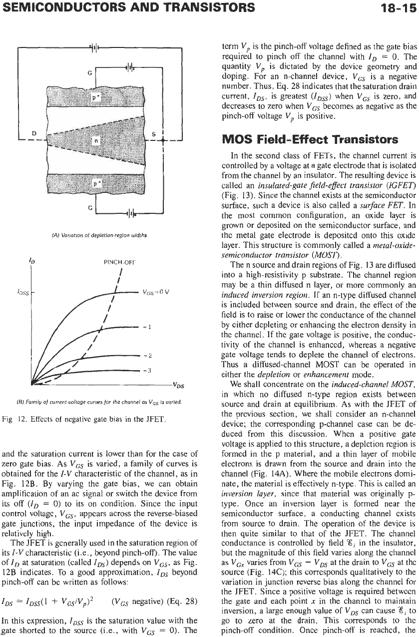
SEMICONDUCTORS AND TRANSISTORS
18-15
GI"1
I
(A)
Variation
of
depletion-region widths
PINCH-OFF
I
I
vDS
(6)
Family
of
current-uoltage
curws
for
the chonnel
as
V,,
is uoried
Fig.
12.
Effects
of
negative gate bias in
the
WET.
and the saturation current is lower than for the case of
zero gate bias.
As
VGs
is varied, a family
of
curves is
obtained for the
I-V
characteristic
of
the channel, as in
Fig.
12B.
By varying the gate bias, we can obtain
amplification
of
an ac signal or switch the device from
its off
(ID
=
0)
to its on condition. Since the input
control voltage,
VGS,
appears across the reverse-biased
gate junctions, the input impedance of the device is
relatively high.
The JFET is generally used in the saturation region of
its
I-V
characteristic (Le., beyond pinch-off). The value
of
I,
at saturation (called
I,)
depends on
Vcs,
as Fig.
12B
indicates. To a good approximation,
IDS
beyond
pinch-off can be written as follows:
I,
=
IDSS(1
+
V~,/V,)~
(v,
negative) (Eq.
28)
In this expression,
1,
is the saturation value with the
gate shorted to the source (i.e., with
Vcs
=
0).
The
term
Vp
is the pinch-off voltage defined as the gate bias
required to pinch
off
the channel with
1,
=
0.
The
quantity
Vp
is dictated by the device geometry and
doping. For an n-channel device,
VGs
is a negative
number. Thus, Eq.
28
indicates that the saturation drain
current,
IDS,
is greatest
(IDss)
when
Vcs
is zero, and
decreases to zero when
Vcs
becomes as negative as the
pinch-off voltage
Vp
is positive.
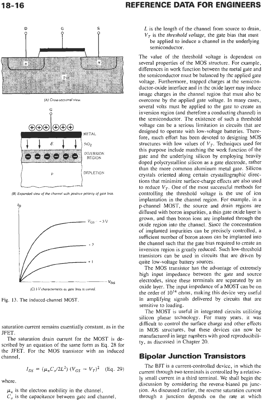
MOS
Field-Effect Transistors
In the second class
of
FETs, the channel current is
controlled by a voltage at a gate electrode that
is
isolated
from the channel by an insulator. The resulting device is
called an insulated-gate jield-effect transistor
(IGFEi")
(Fig.
13).
Since the channel exists at the semiconductor
surface, such a device is also called a surface
FET.
In
the most common configuration, an oxide layer is
grown or deposited on the semiconductor surface, and
the metal gate electrode is deposited onto this oxide
layer. This structure is commonly called a metal-oxide-
semiconductor transistor
(MOST).
The n source and drain regions of Fig.
13
are diffused
into a high-resistivity p substrate. The channel region
may be a thin diffused n layer, or more commonly an
induced inversion region. If an n-type diffused channel
is included between source and drain, the effect
of
the
field is to raise or lower the conductance
of
the channel
by either depleting or enhancing the electron density in
the channel. If the gate voltage is positive, the conduc-
tivity of the channel is enhanced, whereas a negative
gate voltage tends to deplete the channel of electrons.
Thus a diffused-channel
MOST
can be operated in
either the depletion or enhancement mode.
We shall concentrate on the induced-channel
MOST,
in which no diffused n-type region exists between
source and drain at equilibrium.
As
with the JFET of
the previous section, we shall consider an n-channel
device; the corresponding p-channel case can be de-
duced from this discussion. When a positive gate
voltage is applied to this structure, a depletion region is
formed in the p material, and a thin layer of mobile
electrons is drawn from the source and drain into the
channel (Fig.
14A).
Where the mobile electrons domi-
nate, the material is effectively n-type. This is called an
inversion layer, since that material was originally p-
type. Once an inversion layer is formed near the
semiconductor surface, a conducting channel exists
from source to drain. The operation
of
the device is
then quite similar to that of the JFET. The channel
conductance is controlled by field
%,
in the insulator,
but the magnitude of this field varies along the channel
as
V,
varies from
VGs
-
V,
at the drain to
Vcs
at the
source (Fig.
14C);
this corresponds qualitatively to the
variation in junction reverse bias along the channel for
the JFET. Since a positive voltage is required between
the gate and each point x in the channel to maintain
inversion, a large enough value of
VDs
can cause to
go to zero at the drain. This corresponds
to
the
pinch-off condition. Once pinch-off is reached, the
18-16
REFERENCE DATA
FOR
ENGINEERS
D
G
S
(A)
Cross-sectional
ulew.
G
P
Fltl'AL
,
ooolooo
,
il
l
IZ
l
liS'O2
P
DEPLETION
i
(B)
Exponded
dew
of
the channel with
posltiue
polarity
ojgote
bios.
vGs=
L3V
+2
+1
"DS
(C}
I-Vcharacterlstics
as
gate
blas
is
varied
Fig.
13.
The induced-channel
MOST.
saturation current remains essentially constant, as in the
JFET.
The saturation drain current for the MOST is de-
scribed by an equation of the same form as
Eq.
28
for
the JFET. For the
MOS
transistor with an induced
channel,
where,
pn
is
the electron mobility in the channel,
C,
is the capacitance between gate and channel,
L
is the length of the channel from source
to
drain,
V,
is the
threshold
voltage,
the gate bias that must
be applied to induce a channel in the underlying
semiconductor.
The value of the threshold voltage is dependent
on
several properties of the MOS structure. For example,
differences in work function between the metal gate and
the semiconductor must be balanced by the applied gate
voltage. Furthermore, trapped charges at the semicon-
ductor-oxide interface and in the oxide layer may induce
image charges in the channel region that must also be
overcome by the applied gate voltage. In many cases,
several volts must be applied
to
the gate to create an
inversion region (and therefore a conducting channel) in
the semiconductor. The existence of such a threshold
voltage can be a serious limitation in circuits that are
designed
to
operate with low-voltage batteries. There-
fore, much effort has been devoted to designing MOS
structures with low values
of
V,.
Techniques used for
this purpose include matching the work function of the
gate and the underlying silicon by employing heavily
doped polycrystalline silicon as a gate electrode, rather
than the more common aluminum metal gate. Silicon
crystals oriented along certain crystallographic direc-
tions that minimize surface-charge effects are also used
to reduce
V,.
One
of the most successful methods for
controlling the threshold voltage is the use of ion
implantation in the channel region. For example, in a
p-channel MOST, the source and drain regions are
diffused with boron impurities, a thin gate oxide layer is
grown, and then boron ions are implanted through the
oxide region into the channel. Since the concentration
of implanted impurities can be precisely controlled, a
sufficient number of boron atoms can be implanted into
the channel such that the gate bias required to create an
inversion region is greatly reduced. Such low-threshold
transistors can be used in circuits that are driven by
quite low-voltage battery sources.
The MOS transistor has the advantage of extremely
high input impedance between the gate and source
electrodes, since these terminals are separated by an
oxide layer. The input impedance of a MOST can be
on
the order of
loi4
ohms, making this device very useful
in amplifying signals delivered by circuits that are
sensitive
to
loading.
The MOST is useful in integrated circuits utilizing
silicon planar technology. For many years, it was
difficult to control the surface charge and other effects
in
MOS
structures, but these devices can now be
manufactured in large nupbers with good reproducibili-
ty, as discussed
in
Chapter
20.
Bipolar Junction Transistors
The
BJT
is a current-controlled device,
in
which the
current through two terminals is controlled by a relative-
ly small current in a third terminal. We shall begin the
discussion by considering the reverse-biased pn junc-
tion.
As
discussed earlier, the reverse saturation current
through a junction depends
on
the rate at which
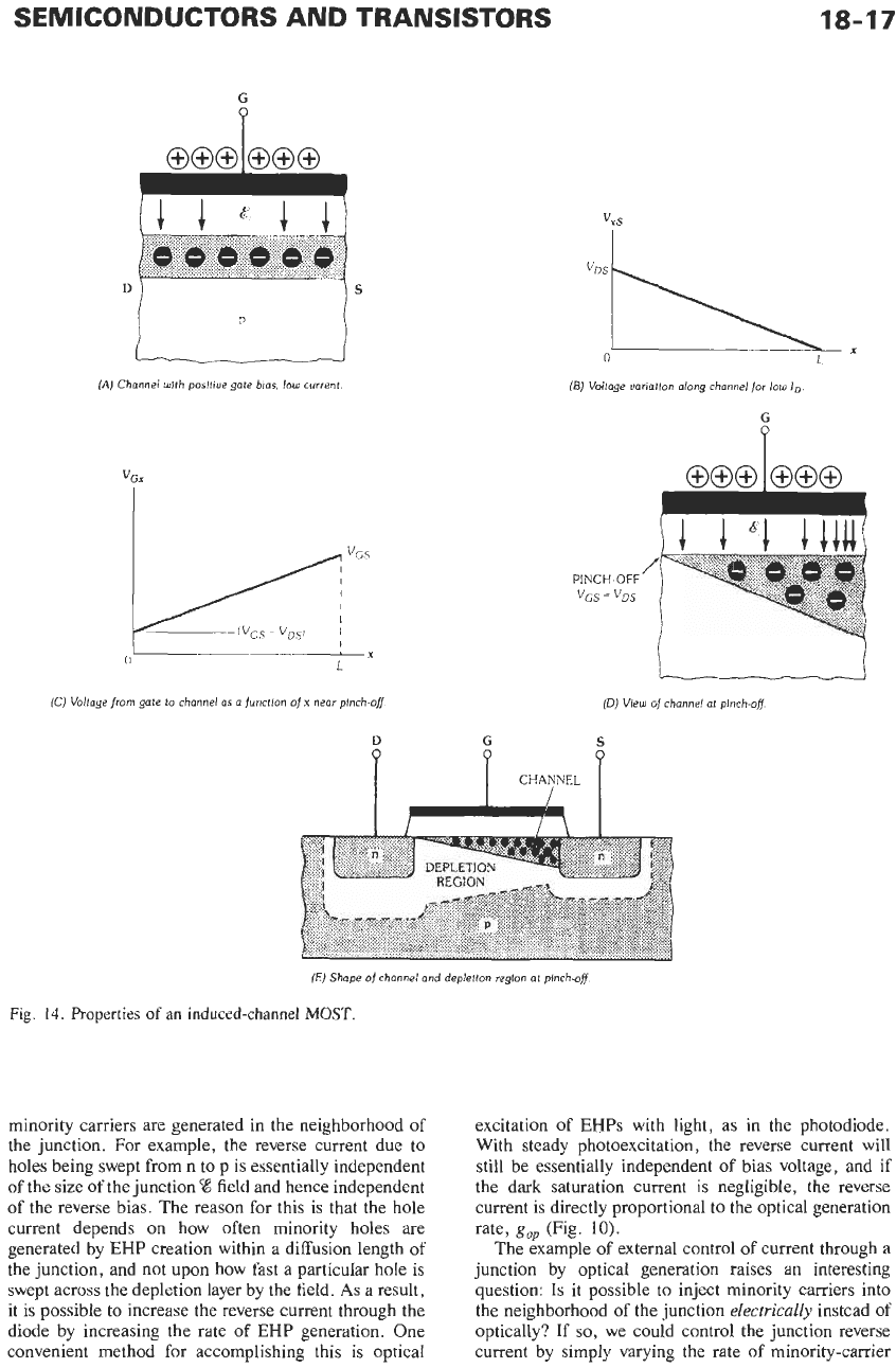
SEMICONDUCTORS AND TRANSISTORS
G
P
il
1
1
11
"i
p
L
(A)
Chonnel with positive gote
bras,
low
current.
18-17
(B)
Voltoge uoriofion
dong
channel
for
low
ID
G
i
000
000
"G,
(C) Voltage
from
gate
to
chonnel
os
a
function
of
x
neor plnch.of
(0)
Vlew of channel
at
pinch-of,
G
P
1-1
I
t
(E)
Shape of channel and depletlon region
ot
plnch-of,
Fig.
14.
Properties
of
an induced-channel
MOST.
minority carriers are generated in the neighborhood of
the junction. For example, the reverse current due to
holes being swept from
n
to
p is essentially independent
of the size of the junction
8
field and hence independent
of the reverse bias. The reason for this is that the hole
current depends
on
how often minority holes are
generated by EHP creation within a diffusion length of
the junction, and not upon how fast
a
particular hole is
swept across the depletion layer by the field.
As
a result,
it
is possible to increase the reverse current through the
diode by increasing the rate of EHP generation. One
convenient method for accomplishing this is optical
excitation of EHPs with light, as in the photodiode.
With steady photoexcitation, the reverse current will
still be essentially independent
of
bias voltage, and if
the dark saturation current
is
negligible, the reverse
current is directly proportional to the optical generation
rate,
g,
(Fig.
10).
The example of external control of current through a
junction by optical generation raises an interesting
question:
Is
it possible to inject minority carriers into
the neighborhood of the junction
electrically
instead of
optically? If
so,
we could control the junction reverse
current by simply varying the rate
of
minority-carrier