Middleton W.M. (ed.) Reference Data for Engineers: Radio, Electronics, Computer and Communications
Подождите немного. Документ загружается.

19
Transistor Circuits
Horace G. Jackson
Device Models and Equations
19-2
Bias Techniques
19-2
Bipolar Transistor
Field-Effect Transistor
Small-Signal Models and Equations
19-5
Single-Stage Amplifiers
19-8
Small-Signal Characteristics
Frequency Response
Large-Signal Characteristics
Output Stages
Harmonic Distortion
Differential Amplifiers
19-17
Current Sources
19-17
Current Mirrors
Active Loads
Feedback Amplifiers
19-18
Basic Properties
Basic Feedback Circuit Topologies
Bandpass Amplifiers
19-22
Single-Tuned Interstage
Double-Tuned Interstage
Sinusoidal Oscillators
19-24
Pulse Circuits
19-26
Pulse Shaping
Multivibrators
19-1
19-2
REFERENCE DATA FOR ENGINEERS
This chapter gives condensed descriptions of many
types of circuits in which transistors are used.
Also
presented
is
design information that makes possible the
determination
of
the various circuit parameters.
In
accordance with the accepted practice, upper-case vari-
ables with upper-case subscripts
(V&)
are used to
indicate the static, or large-signal, quantities, and
lower-case variables with lower-case subscripts
(vce)
are
used
to
indicate the dynamic, or small-signal, values.
The overwhelming majority of transistor circuits are
made with silicon devices; therefore, this is the assumed
technology in this chapter. However, germanium and
gallium-arsenide devices are also available to a limited
degree.
DEVICE MODELS AND
EQUATIONS*
This section presents the basic large-signal circuit
models and equations for three common semiconductor
active devices, namely:
(1)
Bipolar junction transistor (BJT, or simply tran-
(2)
Junction field-effect transistor (JFET or FET)
(3)
Metal-oxide-semiconductor field-effect transis-
The first two are readily found in both discrete and
integrated transistor circuits. Except for some high-
power applications, the third is restricted to integrated
circuits only.
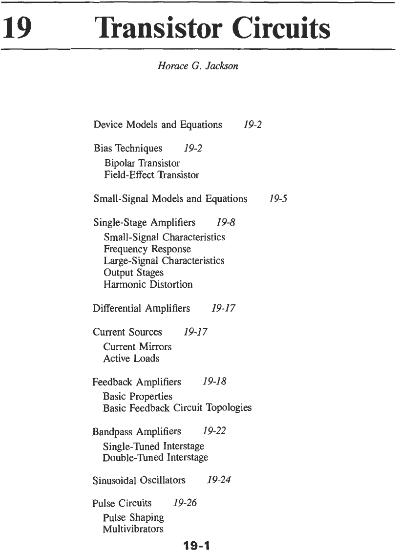
The symbol and large-signal model for an npn
transistor are illustrated in Fig.
1.
For a pnp transistor,
the polarities of the terminal voltages,
VBc, VBE,
and
VFE,
must be reversed; the direction of the junction
diodes must be reversed; and the direction of all the
currents must also be reversed. The model equations are
listed in Chart
1.
Typical values for the device parame-
ters are given in Chart
2.
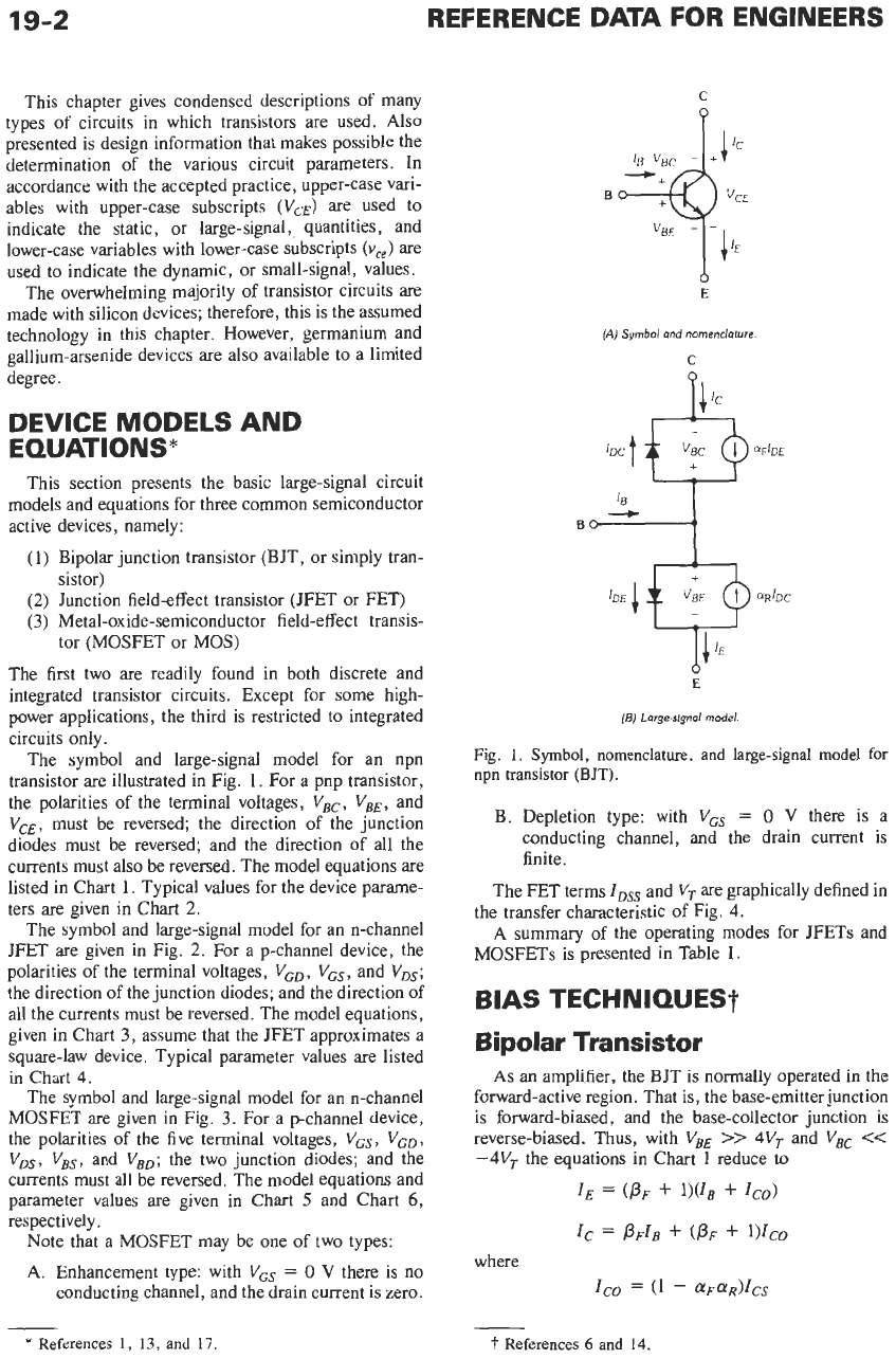
The symbol and large-signal model for an n-channel
JFET are given in Fig.
2.
For a p-channel device, the
polarities of the terminal voltages,
VGD,
Vcs,
and
VDs;
the direction of the junction diodes; and the direction of
all the currents must be reversed. The model equations,
given in Chart
3,
assume that the JFET approximates a
square-law device. Typical parameter values are listed
in Chart
4.
The symbol and large-signal model for an n-channel
MOSFET are given in Fig.
3.
For a p-channel device,
the polarities
of
the five terminal voltages,
Vcs,
VcD,
VDS,
VB~,
and
VBD;
the two junction diodes; and the
currents must
all
be reversed. The model equations and
parameter values are given in Chart
5
and Chart
6,
respectively.
Note that a
MOSFET
may be one of two types:
A.
Enhancement type: with
VGs
=
0
V
there is
no
conducting channel, and the drain current is zero.
sistor)
tor (MOSFET or MOS)
(A)
Symbol and nomenclature.
C
IDCt
$:
viC
0
aFfDE
14
IE
v
E
(B)
Large-slgnal
model.
Fig.
1.
Symbol,
nomenclature,
and
large-signal model
for
npn
transistor
(BJT).
B. Depletion type: with
VGs
=
0
V
there is a
conducting channel, and the drain current
is
finite.
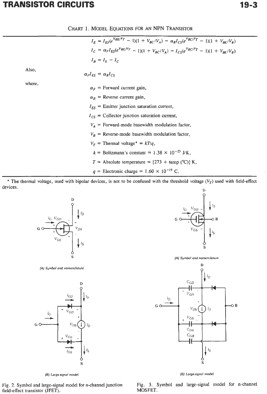
The FET terms
1,
and
V,
are graphically defined in
A
summary of the operating modes for JFETs and
the transfer characteristic of Fig.
4.
MOSFETs is presented in Table
1.
BIAS TECHNIQUES?
Bipolar Transistor
As
an amplifier, the BJT
is
normally operated in the
forward-active region. That is, the base-emitter junction
is forward-biased, and the base-collector junction is
reverse-biased. Thus, with
V&
>>
4VT
and
Vgc
<<
-4VT
the equations in Chart
1
reduce to
I,!?
=
(PF
+
IC
=
PFIB
+
(PF
+
l)ICO
+
IC01
where
Ico
=
(1
-
~~F~RYCS
*
References
1,
13,
and
17.
t
References
6
and
14.
TRANSISTOR
CIRCUITS
19-3
Also,
where.
aF
=
Forward current gain,
aR
=
Reverse current gain,
I,
=
Emitter junction saturation current,
IC-
=
Collector junction saturation current,
VA
=
Forward-mode basewidth modulation factor,
V,
=
Reverse-mode basewidth modulation factor,
V,
=
Thermal voltage*
=
kT/q,
k
=
Boltzmann's constant
=
1.38
X
T
=
Absolute temperature
=
[273
+
temp
("C)]
K,
q
=
Electronic charge
=
1.60
X
J/K,
C.
*
The thermal voltage, used with bipolar devices, is not to be confused with the threshold voltage
(V,)
used with field-effect
devices.
(A)
Symbol and nomenclature.
(Bj
Large-signal model.
Fig. 2. Symbol and large-signal model for n-channel junction
field-effect transistor (JFET).
D
6
s
(A)
Symbol and nomenclature
D
(B)
Large4gnal
model
Fig. 3. Symbol and large-signal model for n-channel
MOSFET.
19-4
REFERENCE
DATA
FOR ENGINEERS
CHART
2.
TYPICAL VALUES
OF
THE
DEVICE
PARAMETERS
FOR
A
LOW-POWER SILICON BJT
(YF
=
0.98
PF
=
(YF/(~
-
(YF)
=
50
aR
=
0.49
PR
=
aR/(1
-
(YR)
=
1
I,
=
1
x
10-14
A
I,
=
2
x
10-14
A
v,
=
20 to 200
v
v,
=
10 to
100
v
VT
=
26
mV
at 27 "C
Good design of the bias circuit for a BJT requires that
two deficiencies of the transistor be overcome. They
are:
1.
The transistor is a temperature sensitive device, in
particular with respect to
VBE
and
PF.
AVBE(T)
=
-2.5
mV/"C
APF(T)
=
+0.7%/"C
Also note that
I,,
doubles for every
8
"C rise in
temperature. But with silicon devices
I,
is
usually
so
small that it may be neglected.
2.
The parameters of a transistor are subject to
process variation, in particular with respect to
PF.
Typically
PF
=
30
to
300
(or greater).
Generally, a constant collector current
I,
and
constant collector-emitter voltage
VcE
are re-
quired. That is, the operating, or quiescent,
point-the Q-point-of the transistor is designed
to be insensitive to temperature and process
variations.
A
self-bias, or emitter bias, circuit is
illustrated in Fig. 5A. The circuit in Fig.
5B
is
the equivalent.
/
VGS
VT
Fig. 4. Typical JFET transfer characteristic.
Given
IC,
VcE,
and
VBE,
the design procedure is as
A. Choose
RE,
where
RE
2
5AVBE/IE.
Here,
AvBE
is the change in
VBE
over the temperature range of
interest. This tends to desensitize the operating
point to temperature variations of
VBE.
B. Determine
RE,
whereRB
5
PFRE15.
Here,
PF
is
the nominal value. This tends to make the
operating point independent
of
variations in the
value
of
PF.
follows:
C. Find
R,,
from
Rc
=
[(Vcc
-
vcE)/IC]
-
RE.
D. Using nominal values for
VBE
and
PF,
solve for
vBB
2:
vBE
+
-k
PFRE)/PFl
In
an
amplifier design,
RE
is usually paralleled by a
capacitor or by a series resistor-capacitor combination.
CHART
3.
MODEL EQUATIONS
FOR
AN
N-CHANNEL JFET
Nonsaturation region,*
VDs
<
(VGx
-
VT):
Saturation region,**
VDs
2
(VGs
-
VT):
where,
ZDss
=
Zero-bias saturation drain current,
i.e.,
VGs
=
0
V,
VDs
>
(VGs
-
VT),
VT
=
Threshold voltage,?
h
=
Channel-length modulation factor.
*
Also
termed the linear, ohmic, or triode region.
**
Also
the constant current, pinchoff, or pentode region.
.F
Also
the pinchoff voltage (V,) or VGs(om. Not to be confused with the thermal voltage (V,) used with bipolar devices.
19-5
CHART
4.
TYPICAL DEVICE PARAMETERS
FOR
A
LOW-
POWER
SILICON JFET
The circuit of Fig. 6A is unsuitable for biasing an
enhancement-type MOSFET, since for an n-channel
device
V,
is positive and it is required that
VGs
>
V,.
N-Channel P-Channel
Two alternative circuits
for
biasing an enhancement-
type MOSFET are included in Fig. 6. In Fig.
6B,
with
negligible gate current
VGS
=
VDs
so
that the transistor
is operating in the saturation region.
RD
=
(VDD
-
VDSYID
IIDssl
1 to 10 mA 1 to
10
mA
+2
to
+6
V
-2
to
-6
V
VT
A
0.1 to
0.01
v-'
0.1
to
0.01
v-'
RG
2
1ORD
Field-Effect
Transistor
When it is required that
VGs
#
VDs,
the circuit in Fig.
6C may be used.
As in the BJT case, in most amplifier applications Rs
is paralleled by a capacitor.
The JFET is also a temperature sensitive device.
AIDss(T)
z
-0.5%/"C
AV,(T)
=
-2
mV/"C
Due to process variations,
ID,
may range
3:l
and
VT
may vary
2:l.
For a MOSFET, the parameters
k
and
V,
have
temperature and process dependence similar to those of
I,
and
VT
for
a JFET.
In designing for a constant
ID
and constant
VDs
in the
saturation region, the self-bias circuit shown in Fig. 6A
can be used with JFETs or depletion-type MOSFETs.
Since the gate current is negligible
SMALL-SIGNAL MODELS AND
EQUATIONS*
For a BJT biased in the forward-active region, the
basic small-signal model for the device is illustrated in
Fig.
7.
Included in the model are the bulk ohmic effects
of the neutral base, collector, and emitter regions,
designated
rb,
r,,
and
re.
Typically, these are about
100
ohms,
50
ohms, and
1
ohm, respectively. The forward-
biased base-emitter junction is modeled by
rli
and
C,,.
CHART
5.
MODEL EQUATIONS
FOR
AN
N-CHANNEL MOSFET
where
k
=
Conduction factor
=
(y~~~/t~~)
(WiL),
y
=
Mobility
of
the conducting carriers,
E,
=
Permittivity
of
the gate oxide,
t,
=
Thickness of the gate oxide,
W
=
Width of the conducting channel,
L
=
Length of the conducting channel,
VT
=
Threshold voltage*
=
V,
+
y[f12qFl
+
lVBsl
-
wl,
V,
=
Zero-bias threshold voltage,
i.e.,
VBs
=
0
V,
2qF
=
Surface potential
0.6
V,
y
=
Body-effect factor,
A
=
Channel-length modulation factor.
*
Not to be confused with the thermal voltage
(V,)
used with bipolar devices.
19-6
REFERENCE
DATA
FOR ENGINEERS
Symbol
V,
Polarity
Vcs
Polarity
VDs
Polarity
cutoff
Region
Region
Saturation
Region
Nonsaturation
TABLE
1.
SUMMARY
OF
OPERATING
MODES
FOR
FET
DEVICES
JFET
N-Channel
G+N
S
Negative
Negative
Positive
vGS
<
vT
P-Channel
G+$
S
Positive
Positive
Negative
vGS
>
vT
CHART
6.
TYPICAL
DEVICE
PARAMETERS FOR A
LOW-
POWER
SILICON
MOSFET
N-Channel P-Channel
k
20(
W/L)pA/VZ
7(W/L)
/.LAW
VTEO
+1
to
+3
v
-1
to
-3
v
VTDO
-1
to
-3
v
+1
to
+3V
(2ppI
-0.6
to
-0.8
V
f0.6
to
+0.8
V
Y
+0.3
to
+0.6
V -0.3
to
-0.6
V
h
0.1
to
0.01
v-1
0.1
to
0.01
v-1
N-Channel
Positive
Positive
Positive
vGS
<
vT
MOSFET
P-Channel
G@B
s
Negative
Negative
Negative
vcs
>
v7
N-Channel
Depletion
G+B
S
Negative
Neg or Pos
Positive
vGS
<
vT
The reverse-biased base-collector junction is modeled
by
C,,
and
r,
is due to the basewidth modulation
effect. That the collector current is a function of the
base-emitter voltage is modeled by current source
g,v,
with output resistance
rce.
How these small-signal
parameters relate to the operating point
of
the transistor
is indicated in Chart
7.
The small-signal model for a JFET biased in the
saturation region is given in Fig.
8.
The ohmic resis-
tances
of
the neutral gate, drain, and source regions are
modeled by the linear resistors
rg,
rd,
and
rs.
Typically,
(A)
SIngle
voltage
supply.
Fig.
5.
Bias circuits for bipolar transistors.
(E)
Tmo-uoltoge-supply
equiuolent.
TRANSISTOR CIRCUITS
"DD
t
19-7
'GS
-
-
(AJ
For JFET
and depletlon-type
MOSFET.
Fig.
6.
Bias
circuits for FETs.
+
(BJ
For
enhancernent4ype
MOSFET
wlth
V,,
=
VGs
+
(C)
Alternative
circuit
for
enhancement
MOSFET
b
E
Fig.
7.
Small-signal model for BJT.
Fig.
8.
Small-signal
model
for JFET.
these are
1
ohm,
10
ohms, and
10
ohms, respectively.
In most applications they may be neglected.
The reverse-biased gate-source and gate-drain junc-
tions of the JFET are modeled by
rgs-Cgs
and
rgd-cgd,
respectively. The voltage-dependent drain-current gen-
erator is modeled by
g,vgs
with an output resistance
of
CHART
7.
SMALL-SIGNAL PARAMETERS FOR A
BJT
rh.
The equations for the latter two parameters are
found in Chart
8.
For low-frequency applications, the charge-storage
elements,
C,,
and
Cgd,
may be neglected. Because
rgs
and
rgd
are generally very large, they also may be
neglected in many applications.
The small-signal model for a MOSFET biased in the
saturation region
is
given in Fig.
9.
The ohmic effects of
the gate, drain, source, and body regions are modeled
by the linear resistors
r,, rd, rs,
and
rb.
Typical values
are
1
ohm,
1
ohm,
1
ohm, and
10
ohms, respectively.
In most applications they may be neglected.
CHART
8.
SMALL-SIGNAL
PARAMETERS
FOR
JFET
19-8
g,
=
1
to
100
mA/V
r,
=
1
to
100
kn
rce
=
0.01
to
1
Mil
C,
=
10
to
100
pF
C,
=
1
to
10
pF
REFERENCE DATA FOR ENGINEERS
g,
=
0.1
to
10
mA/V
rgs
2
io9
Sa
rdS
=
0.01
to
1
Mil
C,,
=
1
to
10
pF
g,
=
0.1
to
10
mAiV
rgs
S_
10’’
n
rds
=
0.01
to
1
Ma
C,,
=
1
to
10
pF
C,d
=
1
to
10
pF
C,,j
=
I
to
10
PF
D
Cdb
G
b
s
Fig.
9.
Small-signal
model
for
MOSFET.
Charge stored between the insulated gate and the
source, drain, and body regions is modeled by the
capacitors
C,,
cgd,
and
Cgb,
respectively. The reverse-
biased source-body and drain-body junctions are in-
generally the resistance values are
so
large that their
effect is usually neglected.
As
with the JFET, the voltage-dependent current
source is modeled by
g,vg,
with an output resistance of
rds.
The equations for these parameters are found in
Chart
9.
The general ranges of the small-signal parameters for
each of the devices considered in this section
are
compared in Table
2.
cluded in the model by
r,b-csb
and
rdb-cdb.
However,
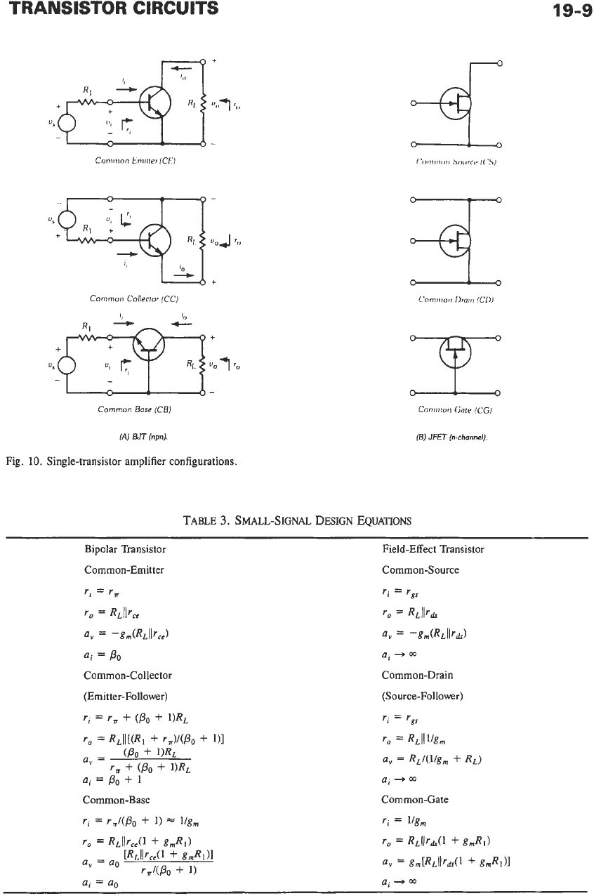
SINGLE-STAGE
AMPLIFIERS*
Small-Signal Characteristics
The three possible circuit configurations for a single-
transistor amplifier are illustrated in Fig.
10.
For
clarity, the bias networks have been omitted. It is
assumed that the bipolar transistor is operating in the
*
References
2,
8,
and
14.
CHART
9.
SMALL-SIGNAL PARAMETERS
FOR
MOSFET
forward-active region and the field-effect transistor is
operating in the saturation region. The small-signal
design equations listed in Table
3
are for the input
resistance
(ri),
output resistance
(ro),
voltage gain
(a,
=
vo/vi),
and current gain
(ai
=
io/ij).
The small-signal
transducer power gain is obtained from
ap
=
a,aj.
The second-order terms due to the bulk ohmic effects
have been omitted. The equations for the FET apply for
both the JFET and the MOSFET. Numerical values for
each of the amplifier configurations are compared in
Table
4.
Frequency Response
In Figs.
11
through
13
are shown simple circuit
schematics for each of the single-stage amplifier config-
urations. Included in each figure are the small-signal
equivalent circuits appropriate for the three ranges of
frequencies, low, middle, and high. The corresponding
small-signal transfer functions derived from the equiva-
lent circuits are listed in Tables
5
through
7.
For the common-emitter and common-source ampli-
fiers, the low cutoff frequency
(-3
dB) is due to the
greater of
oil
or
wL2,
provided the ratio
of
the two is
greater than
10.
In the high-frequency region, normally
frequency
(-3
dB).
For the emitter-follower and the source-follower,
there
is
only one low break frequency. In the high-
frequency region, typically
wZh
is only slightly greater
than
mhl,
though
Wh2
is much greater than either.
Hence, the high cutoff frequency is difficult to deter-
mine accurately. However, it is greater than
whl
,
which
is approximately equal
to
wT
of the transistor.
For
the common-base amplifier, the determination
W,h
>>
062
>>
Whl,
SO
that
Whl
iS the high Cutoff
TRANSISTOR CIRCUITS
19-9
Common
Emitter
(CEJ
---
Common
Collector
(CC)
'I
'0
-
Common
Base
(CBl
fAJ
m'
hnl.
Fig.
10.
Single-transistor amplifier configurations.
(6)
JFET
(n.channel)
TABLE
3.
SMALL-SIGNAL DESIGN EQUATIONS
Bipolar Transistor Field-Effect Transistor
Common-Emitter Common-Source
(Emitter-Follower) (Source-Follower)
ri
=
r,,
+
(Po
+
~)RL
ri
=
rgs
ai
=
a.
ai
+
m