Middleton W.M. (ed.) Reference Data for Engineers: Radio, Electronics, Computer and Communications
Подождите немного. Документ загружается.

18-18
injection. For example, let
us
consider a hypothetical
hole-injection device that can inject holes at a predeter-
mined rate into the
n
side of the junction. The effect
on
the junction current will resemble the effects of optical
generation. The current from
n
to p will depend
on
the
hole injection rate (similar to the reverse current in Fig.
10)
and will be essentially independent of the bias
voltage. There are several obvious advantages to such
external control
of
a current; for example, the current
through the reverse-biased junction would change very
little if the load resistance were altered, since the
magnitude of the junction voltage is relatively unimpor-
tant. Therefore, such an arrangement should be a good
approximation to a controllable constant-current
source.
A
convenient hole-injection device is a forward-
biased p
n
junction (p
+
refers to a very heavily doped p
region). The current in such a junction is due primarily
to holes injected from the p+ region into the
n
material.
If we make the
n
side
of
the forward-biased junction the
same as the
n
side of the reverse-biased junction, the
ptnp structure of Fig.
15
results. With this configura-
tion,
injection of holes from the p’n junction into the
center
n
region supplies the minority-carrier holes
to
participate in the current through the reverse-biased np
junction. Of course, it is important that the injected
holes do not recombine in the
n
region before they can
diffuse
to
the depletion layer of the reverse-biased
junction. Thus we must make the
n
region narrow
compared with a hole diffusion length.
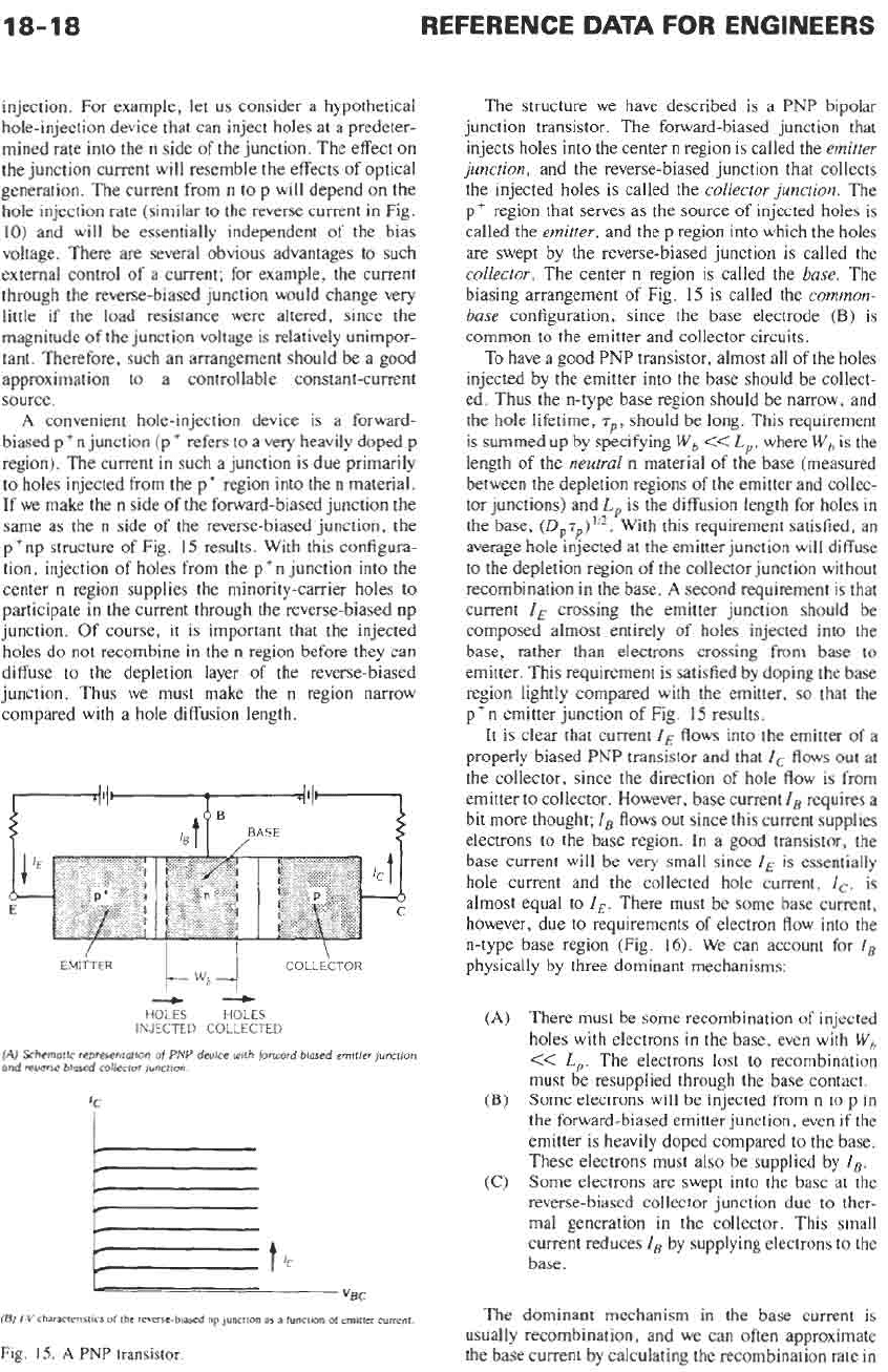
‘5
17”
/BASE
EMITTER COLLECTOR
--
HOLES HOLES
INJECTED COLLECTED
(A)
Schemotlc representation
of
PNP
deuice
with
fomord-blased emitter JUnCtiOn
ond reuerse-blased collector JUnCtiOn.
‘C
“BC
(E)
I-Vcharacteiistics
of
the reverse-biased
np
)unction
as
a
function
of
emitter current.
Fig.
15.
A
PNP
transistor.
The structure we have described is a PNP bipolar
junction transistor. The forward-biased junction that
injects holes into the center
n
region is called the
emitter
junction,
and the reverse-biased junction that collects
the injected holes
is
called the
collector junction.
The
pt region that serves as the source of injected holes
is
called the
emitter,
and the p region into which the holes
are swept by the reverse-biased junction is called the
collector.
The center
n
region is called the
base.
The
biasing arrangement of Fig.
15
is called the
common-
base
configuration, since the base electrode
(B) is
common to the emitter and collector circuits.
To have a good PNP transistor, almost all of the holes
injected by the emitter into the base should be collect-
ed. Thus the n-type base region should be narrow, and
the hole lifetime,
T~,
should be long. This requirement
is summed up by specifying
Wb
<<
L,,
where
Wb
is
the
length of the
neutral
n
material of the base (measured
between the depletion regions of the emitter and collec-
tor junctions) and
L,
is the diffusion length for holes in
the base,
(DP~,)”*.
With this requirement satisfied, an
average hole injected at the emitter junction will diffuse
to the depletion region of the collector junction without
recombination in the base.
A
second requirement
is
that
current
I,
crossing the emitter junction should be
composed almost entirely of holes injected into the
base, rather than electrons crossing from base to
emitter. This requirement is satisfied by doping the base
region lightly compared with the emitter,
so
that the
p’n emitter junction of Fig.
15
results.
It is clear that current
IE
flows into the emitter of a
properly biased PNP transistor and that
IC
flows out at
the collector, since the direction
of
hole flow is from
emitter to collector. However, base current
I,
requires a
bit more thought;
I,
flows out since this current supplies
electrons
to
the base region.
In
a good transistor, the
base current will be very small since
I,
is essentially
hole current and the collected hole current,
I,,
is
almost equal to
I,.
There must be some base current,
however, due to requirements
of
electron flow into the
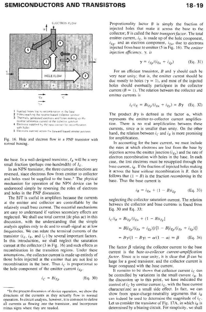
n-type base region (Fig.
16).
We can account for
I,
physically by three dominafit mechanisms:
(A)
There must be some recombination of injected
holes with electrons in the base, even with
Wh
<<
L,.
The electrons lost to recombination
must be resupplied through the base contact.
Some electrons will be injected from n to p in
the forward-biased emitter junction, even if the
emitter is heavily doped compared to the base.
These electrons must also be supplied by
I,.
Some electrons are swept into the base at the
reverse-biased collector junction due to ther-
mal generation in the collector. This small
current reduces
I,
by supplying electrons to the
base.
(B)
(C)
The dominant mechanism in the base current is
usually recombination, and we can often approximate
the base current by calculating the recombination rate in
SEMICONDUCTORS AND TRANSISTORS
18-19
ELECTROk
FLOW
14
&I
- -
'EP
'C
'En
4
1
Injected holes
lost
to recombination
m
the base
2
Holes reaching the reverse biased collector
junction
3
Thermally generated electrons and holes making
up
the
reverse saturation current
of
the collector iunction
4
Electrons supplied
hy
the base contact
for
recombmatton
with
holes
5
Electrons mrected across
the
foiward-biased embttei junction
Fig. 16. Hole
and
electron flow
in
a
PNP
transistor
with
normal biasing.
the base. In a well-designed transistor,
Z,
will be a very
small fraction (perhaps one-hundredth) of
I,.
In
an
NPN
transistor, the three current directions are
reversed, since electrons flow from emitter to collector
and holes must be supplied to the base.* The physical
mechanism for operation of the NPN device can be
understood simply by reversing the roles of electrons
and holes in the PNP discussion.
The BJT is useful in amplifiers because the currents
at the emitter and collector are controllable by the
relatively small base current. The essential mechanisms
are easy to understand if various secondary effects are
neglected. We shall use total current (dc plus ac) in this
discussion, with the understanding that the simple
analysis applies only
to
dc and to small-signal ac at low
frequencies. We can relate the terminal currents of the
transistor
(i,,
i,,
and
ic)
by several important factors.
In this introduction, we shall neglect the saturation
current at the collector (3
in
Fig.
16)
and such effects as
recombination in the transition regions. Under these
assumptions, the collector current is made up entirely of
those holes injected at the emitter that are not lost
to
recombination in the base. Thus
i,
is
proportional to
the hole component of the emitter current
iEp.
*In
the
present discussion
of
device
operation,
we
show the
directions
of
the currents
as
they actually flow
in
normal
operation.
In
circuit
analysis, however,
it
is
common
to
define
all
currents
as
flowing
into
the
transistor,
and
incorporate
minus signs where they are needed.
Proportionality factor
B
is simply the fraction of
injected holes that make it across the base to the
collector;
B
is called the
base transport factor.
The total
emitter current,
i,,
is made
up
of the hole component,
iEp,
and an electron component,
iEn,
due to electrons
injected from base to emitter
(5
in Fig. 16). The
emitter
injection eficiency,
y.
is
For an efficient transistor,
B
and
y
should each be
very near unity; that is, the emitter current should be
due mostly
to
holes
(y
=
11,
and most of the injected
holes should eventually participate in the collector
current
(B
=
1).
The relation between the collector and
emitter currents is
The product
By
is defined as the factor
a,
which
represents the emitter-to-collector current amplifica-
tion. There is no real amplification between these
currents, since
a
is smaller than unity. On the other
hand, the relation between
i,
and
i,
is more promising
for amplification.
In accounting for the base current, we must include
the rates at which electrons are lost from the base by
injection across the emitter junction
(iEn)
and the rate of
electron recombination with holes in the base. In each
case, the lost electrons must be resupplied through the
base current,
i,.
If the fraction of injected holes making
it across the base
without
recombination is
B,
then
it
follows that
(1
-
B)
is the fraction
recombining
in the
base. Thus the base current is
iB
=
i,,,
+
(1
-
B)iEp
(Eq.
33)
neglecting the collector saturation current. The relation
between the collector and base currents is found from
Eq.
30 and
Eq.
33:
The factor
p
relating the collector current to the base
current is the
base-to-collector current-amplijication
factor.
Since
a
is near unity, it
is
clear that
p
can be
large for a good transistor, and the collector current is
large compared with the base current.
It remains to be shown that collector current
ic
can
be controlled by variations in the small current
i,.
In
the discussion up to this point, we have indicated the
control of
i,
by emitter current
i,,
with the base current
characterized as a small side effect.
In
fact, we can
show from space-charge-neutrality arguments that
iB
can indeed be used to determine the magnitude of
i,.
Let
us
consider the transistor of Fig.
17A,
in which
i,
is
determined by a biasing circuit. For simplicity, we shall
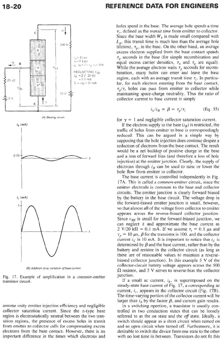
18-20
0
REFERENCE
DATA
FOR ENGINEERS
05-e
1
'B
c-
20
KI!
I-
T"
500
!!
"Ct
li
IO
v
-=
ip
=
10
/!S
7,
=
(1
1
/!S
,C
,R=,j='
'
,,
i,=
lU!l
NEGLECTING
VBi
In
=
2
V
20
k!!
=O
1
mA
Ic=,jiR=
1OmA
,
(A)
Biasing
circuit
ib
(mA)
I
(E)
Addition
of
oc
unriation
of
base
current
Fig.
17.
Example
of
amplification
in
a
common-emitter
transistor
circuit.
assume unity emitter injection efficiency and negligible
collector saturation current. Since the n-type base
region is electrostatically neutral between the two tran-
sition regions, the presence of excess holes in transit
from emitter to collector calls for compensating excess
electrons from the base contact. However, there is an
important difference in the times which electrons and
holes spend in the base. The average hole spends a time
71,
defined as the
transit time
from emitter
to
collector.
Since the base width
W,
is made small compared with
L,,
this transit time is much less than the average hole
lifetime,
T~,
in the base. On the other hand, an average
excess electron supplied from the base contact spends
T~
seconds in the base (for simple recombination and
equal excess carrier densities,
7,
and
7p
are equal).
While the average electron waits
7p
seconds for recom-
bination, many holes can enter and leave the base
region, each with an average transit time
T~.
In
particu-
lar, for each electron entering from the base contact,
7
/7
holes can pass from emitter to collector while
p
.[
maintaining space-charge neutrality. Thus the ratio
of
collector current to base current is simply
i&,
=
p
=
.rp/7(
(Eq.
35)
for
y
=
1
and negligible collector saturation current.
If the electron supply to the base
(i,)
is
restricted, the
traffic of holes from emitter to base is correspondingly
reduced. This can be argued in a simple way by
supposing that the hole injection does continue despite a
reduction
of
electrons from the base contact. The result
would be a net buildup of positive charge in the base
and a loss of forward bias (and therefore a
loss
of hole
injection) at the emitter junction. Clearly, the supply
of
electrons through
i,
can be used to raise or lower the
hole flow from emitter
to
collector.
The base current
is
controlled independently in Fig.
17A. This is called
a
common-emitter
circuit, since the
emitter electrode is common
to
the base and collector
circuits. The emitter junction is clearly forward biased
by the battery
in
the base circuit. The voltage drop in
the forward-biased emitter junction is small, however,
so
that almost all
of
the voltage from collector
to
emitter
appears across the reverse-biased collector junction.
Since
vBE
is small for the forward-biased junction, we
can neglect it and approximate the base current as
2
VI20
kf2
=
0.1 mA. If we assume
7,
=
0.1
ps
and
7,
=
10
ps,
p
for the transistor is 100, and the collector
current
ic
is
10
mA. It is important
to
notice that
i,
is
determined by
p
and the base current, rather than by the
battery and resistor in the collector circuit (as long as
these are of reasonable values to maintain a reverse-
biased collector junction). In this example
5
V
of the
collector-circuit battery voltage appears across the
500
f2
resistor, and
5
V
serves to reverse-bias the collector
junction.
If a small ac current,
ib,
is superimposed on the
steady-state base current of Fig. 1-7, a corresponding ac
current,
i,,
appears in the collector circuit (Fig.
17B).
The time-varying portion of the collector current will be
larger than
ib
.by the factor
p,
and current gain results.
In a switching opertion, a transistor is usually con-
trolled in two conduction states that can be loosely
referred to as the
on
state and the oflstate. Ideally, a
switch should appear as a short circuit when turned
on
and an open circuit when turned
off.
Furthermore, it
is
desirable to switch the device from one state to the other
with no lost time in between. Transistors do not fit this
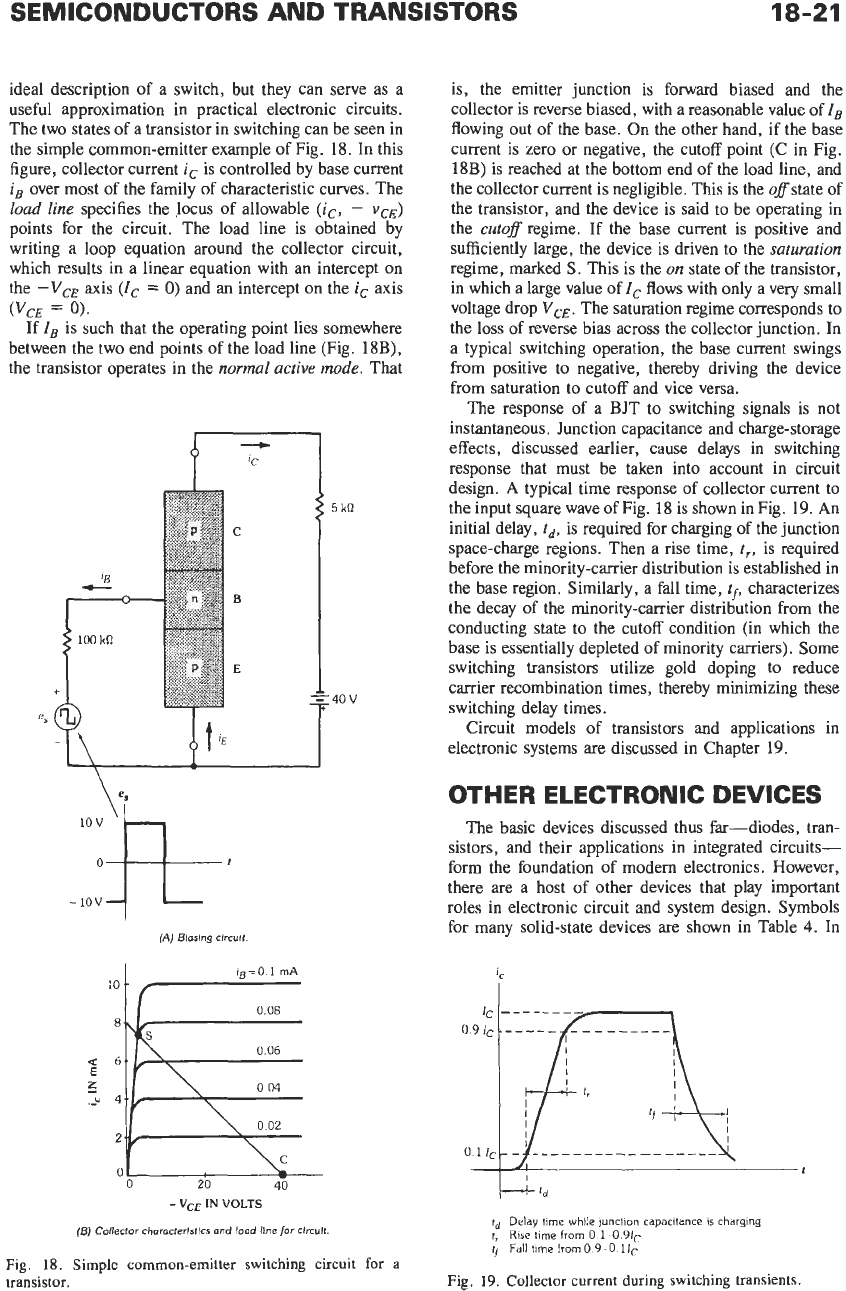
SEMICONDUCTORS AND TRANSISTORS
18-21
ideal description of a switch, but they can serve as a
useful approximation in practical electronic circuits.
The two states of a transistor in switching can be seen in
the simple common-emitter example of Fig. 18.
In
this
figure, collector current
ic
is controlled by base current
iB
over most of the family of characteristic curves. The
load line
specifies the locus of allowable
(ic,
-
vcE)
points for the circuit. The load line is obtained by
writing a loop equation around the collector circuit,
which results in a linear equation with an intercept
on
the
-VcE
axis
(Ic
=
0)
and an intercept
on
the
ic
axis
If
I,
is such that the operating point lies somewhere
between the two end points of the load line (Fig. 18B),
the transistor operates in the
normal active mode.
That
(VCE
=
0).
\
\.;
Q
E
z
.Y
(A)
Blaslng
clrcuit.
lg=0.l
mA
rT
4
2
0
0 20
40
-
V~F
IN
VOLTS
is, the emitter junction is forward biased and the
collector is reverse biased, with a reasonable value of
1,
flowing out of the base. On the other hand, if the base
current is zero or negative, the cutoff point (C in Fig.
18B) is reached at the bottom end
of
the load line, and
the collector current is negligible. This is the oflstate of
the transistor, and the device is said to be operating in
the cutoflregime. If the base current is positive and
sufficiently large, the device is driven to the
saturation
regime, marked
S.
This is the
on
state of the transistor,
in which a large value of
IC
flows with only a very small
voltage drop
VcE.
The saturation regime corresponds to
the loss of reverse bias across the collector junction. In
a typical switching operation, the base current swings
from positive to negative, thereby driving the device
from saturation to cutoff and vice versa.
The response of a
BJT
to switching signals is not
instantaneous, Junction capacitance and charge-storage
effects, discussed earlier, cause delays in switching
response that must be taken into account in circuit
design.
A
typical time response of collector current to
the input square wave of Fig. 18 is shown in Fig. 19. An
initial delay,
td,
is required for charging
of
the junction
space-charge regions. Then a rise time,
t,,
is required
before the minority-carrier distribution is established in
the base region. Similarly, a fall time,
tfi
characterizes
the decay of the minority-carrier distribution from the
conducting state to the cutoff condition (in which the
base is essentially depleted of minority carriers). Some
switching transistors utilize gold doping to reduce
carrier recombination times, thereby minimizing these
switching delay times.
Circuit models of transistors and applications in
electronic systems
are
discussed in Chapter 19.
OTHER ELECTRONIC DEVICES
The basic devices discussed thus far-diodes
,
tran-
sistors, and their applications in integrated circuits-
form
the foundation of modem electronics. However,
there are a host of other devices that play important
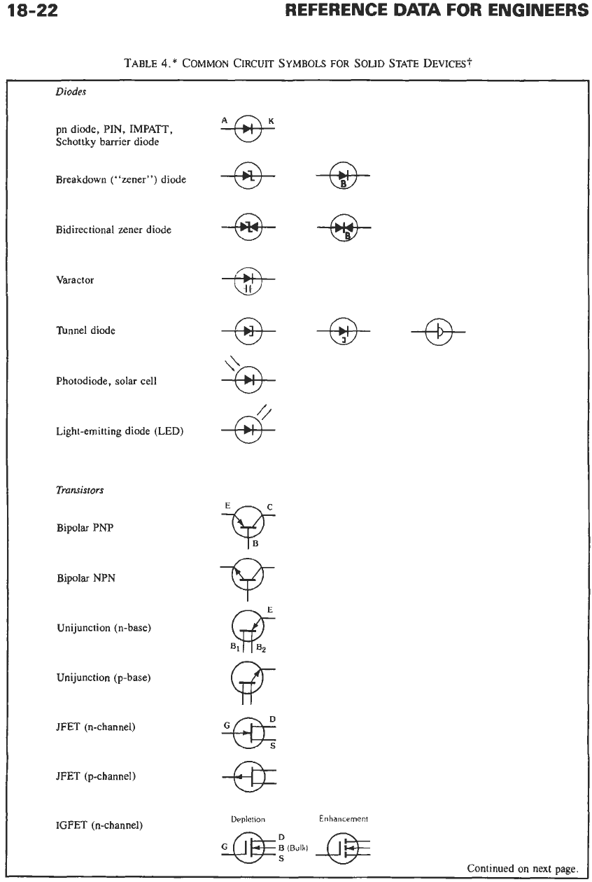
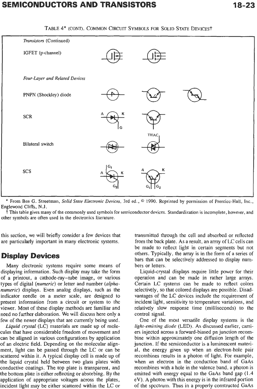
roles in electronic circuit and system design. Symbols
for many solid-state devices are shown in Table
4.
In
__
td
Delay
time while
junction
capacitance is charging
t,
Rise
time
from
0.1-0.91,
t,
Fall
time
from
0
9-0
llc
(B)
Collector
chorocteristlcs
ond
load
line
for
clrcult.
Fig.
18.
Simple common-emitter switching circuit for a
transistor.
Fig.
19.
Collector current during
switching
transients.
18-22
REFERENCE
DATA
FOR ENGINEERS
TABLE
4.*
COMMON
CIRCUIT
SYMBOLS
FOR
SOLID STATE
DEVICES?
Diodes
pn diode,
PIN,
IMPATT,
Schottky barrier diode
Breakdown (“zener”) diode
Bidirectional zener diode
Varactor
Tunnel diode
Photodiode, solar
cell
Light-emitting diode (LED)
Transistors
Bipolar PNP
Bipolar
NPN
Unijunction (n-base)
Unijunction (p-base)
JFET (n-channel)
JFET (p-channel)
IGFET (n-channel)
Enhancement
~
Continued
on
next page.
18-23
TABLE
4'
(CONT).
COMMON
CIRCUIT
SYMBOLS
FOR
SOLID
STATE
DEVICES?
Transistors
(Continued)
IGFET
(p-channel)
Four-Layer and Related Devices
PNPN (Shockley) diode
SCR
Bilateral switch
scs
*
From Ben
G.
Streetman,
Solid State Electronic Devices,
3rd ed.,
Q
1990.
Reprinted
by
permission
of
Prentice-Hall, Inc.,
t
This table gives many
of
the commonly used symbols
for
semiconductor devices. Standardization
is
incomplete, however, and
Englewood Cliffs,
N.J.
other
symbols
are often used in the electronics literature.
this section, we will briefly consider a few devices that
are particularly important in many electronic systems.
Display Devices
Many electronic systems require some means of
displaying information. Such display may take the form
of a printout, a cathode-ray-tube image, or various
types of digital
(numeric)
or letter and number
(alpha-
numeric)
displays. Even analog displays, such as the
indicator needle on a meter scale, are designed to
present information from a circuit or system to the
viewer. Most of these display methods are familiar and
need
no
further elaboration. We will discuss here only a
few of the newer displays that are currently being used.
Liquid
crystal
(LC) materials are made up
of
mole-
cules that have considerable freedom of movement and
can be aligned in various configurations by application
of
an
electric field. Depending
on
the molecular align-
ment, light can be passed through the
LC
or can be
scattered within it.
A
typical display cell is made up of
the liquid crystal held between two glass plates with
conductive coatings. The top plate is transparent, and
the bottom plate is either reflecting
or
absorbing. By the
application of appropriate voltages across the plates,
incident light may be either scattered within the LC or
transmitted through the cell and absorbed or reflected
from the back plate. As a result, an array of LC cells can
be made to reflect light in certain segments but not
others. Typically, the array is in the form of a series of
bars that can be selectively addressed to display num-
bers or letters.
Liquid-crystal displays require little power for their
operation and can be made in rather large arrays.
Certain LC systems can be made to reflect colors
selectively,
so
that colored displays
are
possible. Disad-
vantages of the LC devices include the requirement of
incident light, sensitivity to temperature variations, and
relatively slow response time (milliseconds) to the
control signal.
One of the most versatile display systems is the
light-emitting
diode
(LED).
As
discussed earlier, carri-
ers injected across a forward-biased pn junction recom-
bine within approximately one diffusion length of the
junction.
If
the semiconductor is a luminescent materi-
al, the energy given up when an electron-hole pair
recombines results in a photon of light. For example,
when
an
electron in the conduction band of GaAs
recombines with a hole in the valence band, a photon is
emitted with energy equal to the GaAs band gap (1.4
eV). A photon with this energy is in the infrared portion
of the spectrum. Thus in a properly constructed
GaAs
18-24
junction, forward bias results in considerable carrier
injection, recombination, and the resulting emission of
infrared light. The intensity of the light can be varied
(with nanosecond response time) by changing the diode
current; thus electrical signals can be converted into
optical signals by the LED. Used in conjunction with a
photodiode, the LED can send information from one
point
to
another optically. Another application
of
the
LED-photodiode is in an
isolator.
Since the signal
transmission is optical, complete electrical isolation can
be achieved. Such an isolator pair can be mounted on an
insulating substrate and packaged to form a device that
allows signal transfer between input and output while
maintaining electrical isolation.
If the information receiver is the human eye, the
display device must emit light in the visibleopart of the
spectrum (approximately
4000
to
7000
A in wave-
length, or 3.1 to 1.8 eV in photon energy). Visible
LEDs are built that cover the range from red to green.
For example, the compound GaAsP has a band gap that
can be varied from that of GaAs (1.4 eV)
to
that of GaP
(2.3 eV) by choosing the appropriate mixture. When
the phosphorus content is about 40% of the column V
constituent, the band gap is 2 eV, in the red. This is the
most common material for LED display fabrication. By
using segments made up of GaAsP strips, a numeric
display can be made that emits light in the appropriate
segments
to
display numbers or letters. Such an LED
display operates at very low voltage, has a long opera-
ting lifetime, and is highly reliable.
Microwave Devices
The use of transistors at high frequencies is generally
limited to the range of a few gigahertz by capacitance
and transit-time effects. Therefore, generation and
amplification of microwave signals usually depend on
special devices that can deliver high-frequency ac power
to a resonant cavity or waveguide. Power is delivered to
an ac signal if there is an increase in the motion of
charge through a region where the field is changing such
as
to
retard such motion. For charges in a solid or gas,
this is called
negative differential conductivity.
As an
example, suppose holes are drifting down a typical
semiconductor bar in the direction of an electric field. If
the field varies with time, the holes speed up or slow
down as the field changes, and power is extracted from
the field. However, if the arrival of holes at a certain
point were to increase during a time interval in which
the field at that point decreases, power would be
delivered to the field, and the apparent conductivity
dll&
would be negative. The object of microwave
oscillators is
to
modulate the rate of arrival of electrons
or holes at a point where the electric field is varying,
such that the arrival coincides with the retarding half-
cycle of the ac field.
A
number of solid-state microwave devices have been
introduced in recent years. Most of these devices are
variations
of
the
IMPATT
diode
and the
gunn
diode.
In
each of these devices, a negative conductance allows
current oscillations that can be used to generate micro-
wave signals.
The negative conductance in
an
IMPATT diode
results from avalanche multiplication and transit-time
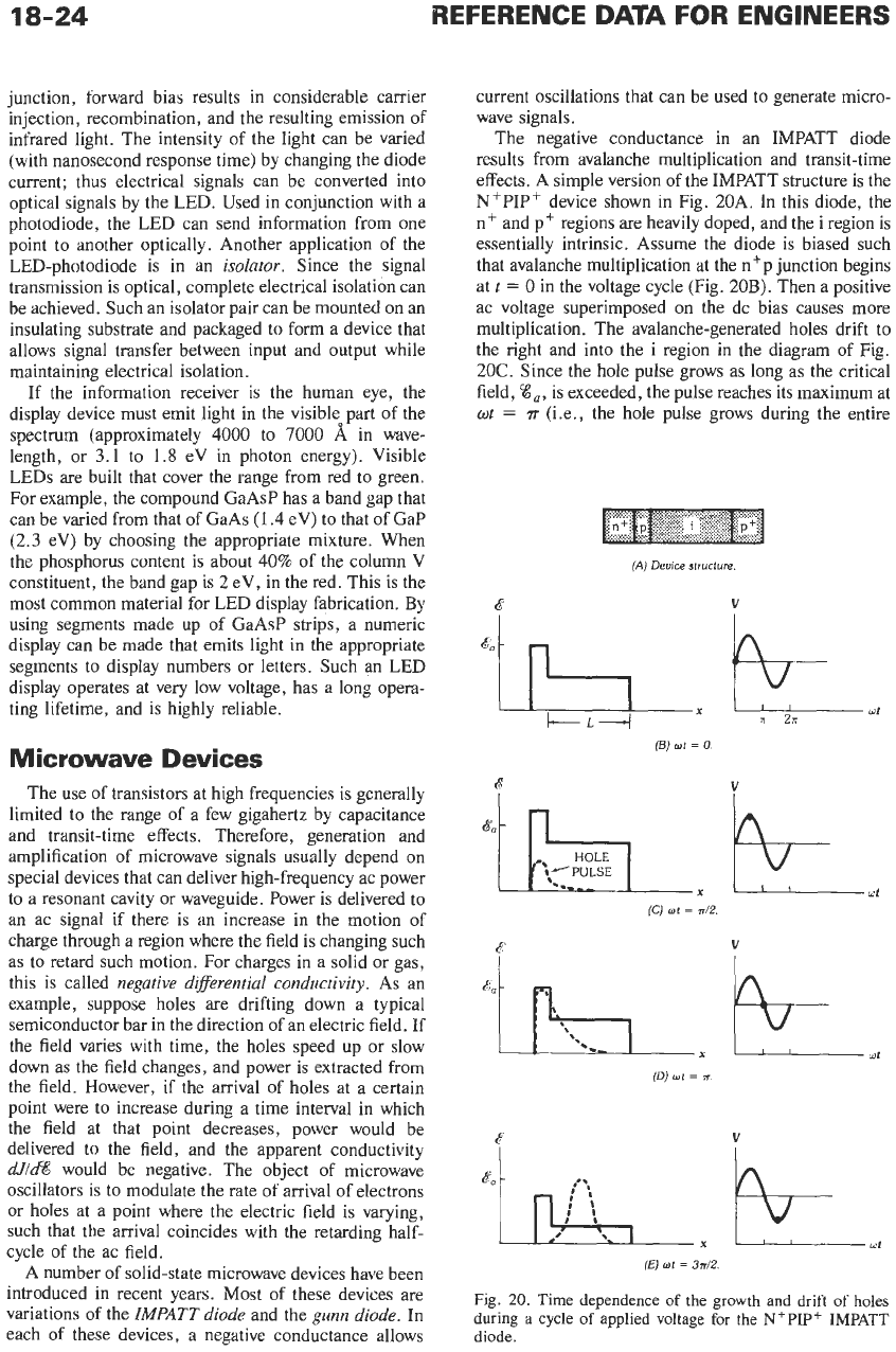
effects. A simple version of the IMPATT structure is the
N'PIP' device shown in Fig. 20A. In this diode, the
nt and pt regions are heavily doped, and the
i
region is
essentially intrinsic. Assume the diode is biased such
that avalanche multiplication at the n 'p junction begins
at
t
=
0
in the voltage cycle (Fig. 20B). Then a positive
ac voltage superimposed on the dc bias causes more
multiplication. The avalanche-generated holes drift to
the right and into the i region in the diagram of Fig.
20C. Since the hole pulse grows as long as the critical
field,
ga,
is exceeded, the pulse reaches its maximum at
at
=
?r
(i.e., the hole pulse grows during the entire
(CJ
ut
=
d2.
V
(Dj
ot
=
R
c
V
(EJ
ot
=
3d2.
Fig.
20.
Time dependence
of
the growth and drift
of
holes
during a
cycle
of
applied voltage
for
the N'PIP' IMPATT
diode.
SEMICONDUCTORS AND TRANSISTORS
18-25
positive half-cycle of the voltage). Then as
v
enters its
negative half-cycle, avalanche ceases at the n'p junc-
tion (Fig.
20D).
However, the hole pulse drifts through
the i region from left to right while the ac terminal
voltage is negative. Since the holes
are
collected during
the negative half-cycle of voltage, the ac conductance is
negative during this period. If length
L
is chosen such
that the pulse drifts through the i region for the full
negative half-cycle of voltage, negative conductance
will be obtained for the entire half-cycle. The IMPATT
device can be placed in a resonant cavity tuned to the
appropriate frequency, and microwave generation re-
sults.
Current pulses
are
created in a GaAs gunn diode by a
mechanism that transfers electrons from one region of
the conduction band to another. The conduction elec-
trons in GaAs normally reside in a band
1.43
eV above
the valence band. In addition, a subsidiary conduction
band lies about
0.3
eV above the first. Of course, this
higher-lying band is generally of little interest, since
conduction-band electrons are usually found only in the
lower-energy band. It
is
possible, however, to excite
electrons into the upper conduction band by applying a
sufficiently large electric field. The reason this transfer
is of interest is that the mobility of electrons in the
upper band is much smaller than the usual mobility of
electrons in the lower conduction band. Thus, when
electrons are transferred to the low-mobility subsidiary
band, they actually
slow
down.
At a critical threshold
field,
gth,
electrons begin to transfer to the upper band,
(A)
Reuerse
blocking state.
+
-
I
I
I\
11
+.
(B)
Forward blocking state.
I
I+
(C)
Forward conducting state.
I2
13
(0)
Addition
of
gate
to
form
SCR
Fig.
21,
Biasing
of
a
PNPN
device.
18-26
where their velocity is smaller. This transfer results in a
negative differential conductance that can be used in
microwave generation.
Switching Devices
Many electronic applications call for a device that can
be switched from a nonconducting
“off’
state to a
conducting
“on”
state. Several devices can be used in
switching applications, and selection of the appropriate
device depends
on
requirements of power level, switch-
ing time, and other factors. A common electronic
switch
is
the bipolar transistor, which can be driven
from cutoff to saturation by controlling the small base
current, or the FET, which can be switched by control-
ling the gate voltage.
The most widely used controllable switch for large
currents is the
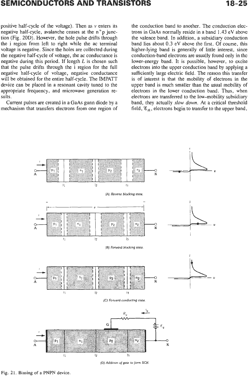
semiconductor controlled recti$er (SCR).
This is a four-layer PNPN device (Fig. 21) with
terminals attached to the anode (A) and the cathode (K)
and a third terminal attached to one of the central
regions. This third terminal is called the gate (G).
When the gate is left open, the SCR has the characteris-
tic of Figs. 21A-C. With a negative applied voltage,
junctions
j,
and j, are reverse biased (Fig. 21A), and
current through the device is effectively blocked, even at
high reverse voltage. With a positive voltage (A positive
with respect
to
K),
junctions j, and j3 are forward
biased, while
j,
is reverse biased (Fig. 21B). Initially,
the device current is restricted to the small saturation
current of j,. This is called the
forward blocking state
and corresponds
to
the
“off’
condition of the switch.
The SCR can be thought of as two coupled transistors
(plnlp2 and n,p2n2) with a common collector junction,
j,. If transistor action is initiated, holes injected into n
I
from the forward-biased emitter junction, j
,,
can be
transported across the base of the PNP structure into p,.
Such transistor action in effect feeds holes into the base
of the NPN structure, thereby increasing electron injec-
tion from n2 into p2. Such injected electrons can then
be collected across j, into n, by transistor action, and
the process continues. The result is a combination of
two saturated transistors, typified by high current at low
voltage (the
forward conducting state),
as shown in Fig.
21c.
The initiation of transistor action (and therefore
switching) can occur as a result of raising the bias to a
critical value
(V,).
At this voltage, avalanche multipli-
cation at j, and base-width narrowing* in
nI
and p2
combine
to
initiate transport of minority carriers across
the two base regions. Alternatively, a small gate current
i,
can supply sufficient base current to the NPN structure
to
initiate transitor action (Fig. 21D). The latter switch-
ing method is the most common type for an SCR. In
this mode of operation, the device is nonconducting at
*Base-width narrowing occurs
as
the
depletion region
about
j,
grows
due
to
the
increased
reverse bias.
As
the
effective
widths
of
n,
and
p2
become
smaller,
base
transport
factor
B
increases.
-
fonvard voltages until a small pulse
of
current is applied
to the gate. Such a pulse initiates transistor action in the
device and switches it into the conducting state. The
SCR remains in the conducting state until current
I
is
dropped below a value called the
holding current
required to maintain transistor action. In addition, some
SCR
devices can be turned off by applying a negative
current to the gate, thereby extracting carriers and
terminating the transistor action within the device.
REFERENCES
Semiconductor Physics
Blakemore, J.
S.
Semiconductor Statistics.
New York:
Dover Publications, 1987.
Ferry, D. K.
Semiconductors.
New York: Macmillan,
1991.
Hess,
K.
Advanced Theory of Semiconductor Devices.
Englewood Cliffs, N.J.: Prentice Hall, 1988.
Shur,
M.
GaAs Devices and Circuits.
New York:
Plenum Press, 1987.
Shur, M.
Physics of Semiconductor Devices.
Englewood
Cliffs, N.J.: Prentice Hall, 1990.
Wang
,
S
. Fundamentals
of
Semiconductor Theory and
Device Physics.
Englewood Cliffs, N.J.: Prentice
Hall, 1989.
Wolfe,
C.
M., Holonyak, N., and Stillman, G.
E.
Physical Properties of Semiconductors.
Englewood
Cliffs, N.J.: Prentice Hall, 1989.
Junctions and Transistors
Capasso, F., and Margaritondo,
G.
eds.
Heterojunction
Band Discontinuities: Device Physics and Applica-
tions.
New York: North Holland, 1987.
Jaeger, R.
C.
The Modular Series on Solid State
Devices,
Vol.
V:
Introduction to Microelectronic
Fabrication.
Reading, Mass.
:
Addison-Wesley
,
1988.
Muller, R.
S.,
and Kamins, T. I.
Device Electronics for
Integrated Circuits.
2d ed. New York: John Wiley,
1986.
Roulston,
D.
J.
Bipolar Semiconductor Devices.
New
York: McGraw-Hill, 1990.
Sze,
S.
M.
High-speed Semiconductor Devices.
New
York: John Wiley, 1990.
Sze,
S.
M.
Semiconductor Devices: Physics and Tech-
nology.
New York: John Wiley, 1985.
Wang, C.
T.
Semiconductor Technology: GaAs and
Related Compounds.
New York: John Wiley, 1990.
Warner, R.
M.,
and Grung, B.
L. Semiconductor-
Device Electronics.
Philadelphia: Holt, Rinehart
and Winston, 1991.
Wolf,
S.,
and Tauber,
R.
N.
Silicon Processing for the
VLSI
Era.
Sunset Beach, Calif.: Lattice Press,
1986.
18-27
Yang, E.
S.
Microelectronic Devices.
New York:
McGraw-Hill, 1988.
Optoelectronic Devices
Agrawal, G. P., and Dutta, N.
K.
Long-Wavelength
Semiconductor Lasers.
New York Van Nostrand
Reinhold, 1989.
Cheo, P. K.
Fiber Optics and Optoelectronics.
Engle-
wood Cliffs, N.J.: Prentice Hall, 1990.
Coutts,
T.
J., and Meakin, J. D.
Current Topics in
Photovoltaics.
New York: Academic, 1985,
Gowar, J.
Optical Communication Systems.
Englewood
Cliffs, N.J.: Prentice Hall, 1984.
Miller,
S.
E., and Kaminow,
I.
P. eds.
Optical Fiber
Telecommunications
II.
San Diego: Academic
Press, 1988.
Nishihara, H., Haruna, M., and Suhara,
T.
Optical
Integrated Circuits.
New York McGraw-Hill,
1989.
Senior, J.
Optical Fiber Communications.
Englewood
Cliffs, N.J.: Prentice Hall International, 1985.
Wilson, J., and Hawkes, J.
F.
B.
Optoelectronics.
2nd
ed. Cambridge: Prentice Hall International, 1989.
Microwave Devices
Blakey, P. A., East, J. R., and Haddad, G.
1.
“Impact
of Submicron Technology on Microwave and
Millimeter-wave Devices.”
VLSI Electronics: Mi-
crostructure Science.
Vol. 2. New York Academic
Press, 1981. Ch. 4, pp. 105-147.
Bosch, B. G., and Engelmann, R. W. N.
Gunn
Efsect
Electronics.
New York: John Wiley-Halstead
Press, 1975.
Bulman, P. J., Hobson, G.
S.,
and Taylor, B. C.
Transferred Electron Devices.
New York Academ-
ic Press, 1972.
Capasso,
F.,
and Margaritondo, G., eds.
Hetero-
junction Band Discontinuities: Device Physics and
Applications.
New York North Holland, 1987.
Ferry, D.
K.,
ed.
Gallium Arsenide Technology.
Indian-
apolis: Howard W.
Sams
&
Co., 1985.
Gibbons, G.
Avalanche-Diode Microwave Oscillators.
Oxford: Clarendon Press, 1973.
Hobson, G.
S.
The Gunn Efsect.
Oxford: Clarendon
Press, 1974.
Liao,
S.
Y.
Microwave Devices and Circuits.
Engle-
Sze,
S.
M.
High-speed Semiconductor Devices.
New
wood Cliffs, N.J.: Prentice Hall, 1980.
York: John Wiley, 1990.
Semiconductor Controlled
Rectifiers
Blicher, A.
Thyristor Physics.
New York: Springer-
Verlag
,
1976.
Gentry,
F.
E., Gutzwiller,
F.
W., Holonyak, N., Jr.,
and Von Zastrow, E. E.
Semiconductor Controlled
Rect$ers: Principles and Application
of
p-n-p-n
Devices.
Englewood Cliffs, N.J.: Prentice Hall,
1964.
Ghandi,
S.
K.
Semiconductor Power Devices,
New
York: John Wiley, 1977.
Special Issue
on
High-Power Semiconductor Devices,
IEEE Transactions
on
Electron Devices
ED-23,
no.
8
(August 1976).
Laster, C.
Thyristor Theory and Application.
Blue
Ridge Summit, Pa.: Tab Books, 1986.
Sze,
S.
M.
Physics
of
Semiconductor Devices.
New
York John Wiley, 1981.
Taylor, P.
D.
Thyristor Design and Realization.
Chichester: John Wiley, 1987.
General
Allison, J.
Electronic Engineering Semiconductors and
Devices.
London: McGraw-Hill, 1990.
Beadle, W. E., Tsai, J.
C.
C., and Plummer, R. D.,
eds.
Quick Reference Manual for Silicon Integrated
Circuit Technology.
New York: John Wiley-
Interscience, 1986.
Dalven, R.
Introduction
to
Applied Solid State Physics.
2nd ed. New York: Plenum, 1990.
Kittel,
C.
Introduction to Solid State Physics.
6th ed.
New York: John Wiley, 1986.
Pierret,
R.
F.,
and Neudeck, G. W.
Modular Series
on
Solid State Devices.
Reading, Mass.
:
Addison-
Wesley Publishing Co., Inc., 1983.
Streetman, B. G.
Solid State Electronic Devices.
3rd
ed. Englewood Cliffs, N.J.: Prentice Hall, Inc.,
1990.
Sze,
S.
M.
Physics
of
Semiconductor Devices.
2nd ed.
New York: John Wiley
&
Sons,
Inc., 1981.