Middleton W.M. (ed.) Reference Data for Engineers: Radio, Electronics, Computer and Communications
Подождите немного. Документ загружается.

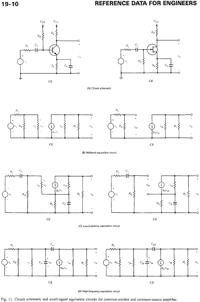
19-10
REFERENCE
DATA
FOR
ENGINEERS
+
CE
*
CS
(A)
Clrcult schematic.
CE CS
(E)
Midband equivalent clrcuit.
CE
cs
(C)
Low-frequency equfuoient cIrcuIt.
CE
cs
(0)
High-frequency equivalent cfrcuit
Fig.
1
1.
Circuit schematic and small-signal equivalent circuits
for
common-emitter and common-source amplifier.
TRANS ISTOR CI RCU ITS
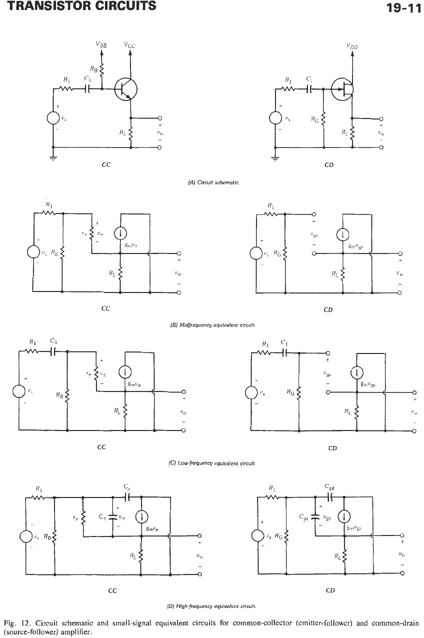
19-11
(A)
Clrcult schematic.
KI
R1
"DD
t
cc
(B)
Mldfrequency equlualent circuit
R,
c1
CD
cc
CD
(C)
Lowfrequency equlualent drcult.
cc
CD
(D)
Hlgh-frequency equlualent clrcult.
Fig.
12.
Circuit schematic and small-signal equivalent circuits for common-collector (emitter-follower) and common-drain
(source-follower) amplifier.
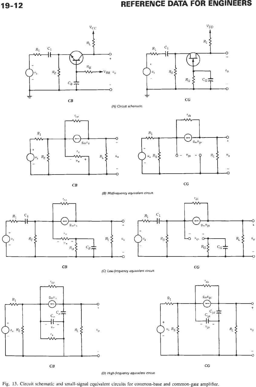
19-12
.
RE
::
REFERENCE
DATA
FOR ENGINEERS
+
-
+
us
RS
::
-
vcc
t
+
CB
(A)
Circuit schemotlc.
9
CG
CB CG
(C) Low.frequency equiualent circuit.
'dr
CB
CG
(D)
High-frequency equivalent circuit.
Fig.
13.
Circuit schematic and small-signal equivalent circuits
for
common-base and common-gate amplifier.
TRANS
I
STO
R
CI
RC
U
ITS
r,
ro
a,
ai
Circuit
Data
19-13
BJT
FET
CE
cc
CB
cs
CD CG
1.3
kn
256
kn
26
io9
n
109
n
224
5
kfl
120
n
5
kn
5
kM
214
5
kn
-
192
0.99
188
-
22 0.96
22
1
.o
50
51
0.98
- -
R,
=
5
kn,
R,
=
5
kfi
RI
=
5
kn,
RD
=
5
kn
I,
=
1 mA
Po
=
50,
VA
=
50
V
I,
=
1
mA
I,
=
5
mA,
V,
=
-1
V,
V,
=
50
V
TABLE
4.
COMPARISON OF SMALL-SIGNAL
AMPLIFIER
PARAMETERS
TABLE
5.
SMALL-SIGNAL
TRANSFER
FUNCTIONS:
COMMON-EMITTER
AND COMMON-SOURCE
Bipolar Transistor
Midfrequency
a0
=
vJvS
=
-gm(R~llrce)[rff/(RI
+
r,)l
Low Frequency
1. Due to
C,
(assume that
CE
is a short-circuit)
a,(jw)
=
ao/(l
-
jwJllo)
where,
oil
i5-
U(RI
+
ra)C1
2. Due
to
CE
(assume that
CI
is a short-circuit)
a,(jw)
=
ao(1
+
jwlwzJ(l
+
jwlq2)
where,
w,/
==
l/RECE
WJZ
High Frequency
~/IREII[(RI
+
r,)KPo
+
l)l}C~
Field-Effect Transistor
Midfrequency
ao
=
v0/vS
=
-gm(RLllrds)[RG/(Ri
+
RG)~
Low Frequency
1. Due to
Cl
(assume that
Cs
is a short-circuit)
a,(jw)
=
ao/(l
-
jwJ,/w)
where,
oL1
==
l/(R,
+
RG)C,
2.
Due to
C,
(assume that
C,
is a short-circuit)
a,(jo)
=
ao(l
+
jw/wzl)l(l
+
jwlolz)
where,
~,i
i5-
1IRSCs
012
i=
1/[RSll(1/gm)lcS
High Frequency
19-14
REFERENCE
DATA
FOR ENGINEERS
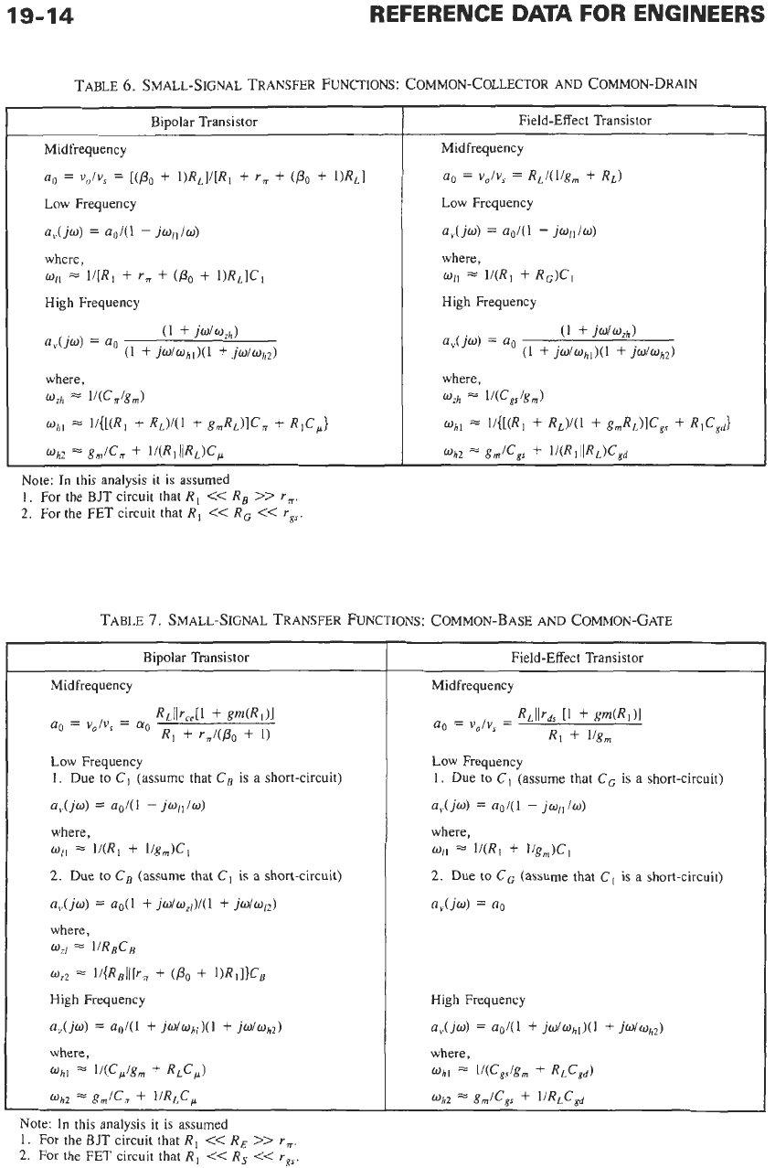
TABLE
6.
SMALL-SIGNAL
TRANSFER
FUNCTIONS:
COMMON-COLLECTOR AND
COMMON-DRAIN
Bipolar Transistor Field-Effect Transistor
Mid frequency Mid frequency
a.
=
v,/v,
=
[(Po
+
l)RL]l[Rl
+
ra
+
(PO
+
W1
Low Frequency Low Frequency
a.
=
v,/v,
=
RLl(llgm
+
RJ
I
High Frequency
av(jw)
=
ao/(l
-
jwl,/w)
where,
WII
E
l/(Rl
+
R,)Cl
High Frequency
aJj4
=
a0
(1
+
jwl%h)
(1
+
jw/ohl)(l
+
jwlwhz)
TABLE
7.
SMALL-SIGNAL
TRANSFER
FUNCTIONS:
COMMON-BASE
AND
COMMON-GATE
Bipolar Transistor
Midfrequency
Low Frequency
1,
Due
to
C,
(assume that
C,
is a short-circuit)
a,(jw)
=
q/(l
-
joll/w)
where,
~11
z
lI(R1
+
l/g,)CI
2.
Due
to
C, (assume
that
C,
is a short-circuit)
a,(jw)
=
ao(l
+
jw/wzl)/(l
+
jw/o12)
where,
Oii
l/RBCs
'32
li{RBl/[r,
+
(Po
I)RII)CB
High Frequency
a,(jo)
=
ao/(l
+
jdwhl)(l
+
jw/wh2)
where,
whl
l/(Cp/gm
+
RLCp)
whz
E
g,/C,
+
IIRLC,
Note:
In
this analysis it is assumed
1.
For the BJT circuit that
R,
<<
RE
>>
r,,.
2.
For
the FET circuit that
R,
<<
R,
<<
rgs.
Field-Effect Transistor
Mid frequency
Low Frequency
1.
Due
to
C,
(assume that
CG
is a short-circuit)
a,(jw)
=
q/(l
-
jwl,lw)
where,
011
z
1/(Rl
+
I/g,)C,
2. Due
to
CG
(assume that
C,
is
a
short-circuit)
a,W
=
a0
High Frequency
a,(jw)
=
ao/(l
+
jwlwhl)(l
+
jw/wh2)
where,
oh1
1/(cgx18m
+
RLCgd)
Oh2
gmIcm
+
IIRLC,d
TRANSISTOR CIRCUITS
19-15
of the low cutoff frequency is similar to the case of
the common-emitter amplifier. However, note that for
the common-gate amplifier there is only one low
break frequency. In the high-frequency region, typ-
ically
wh2
>>
oh]
so
that
oh,
is the high cutoff
frequency.
Large-Signal Characteristics
For large-signal operation, both bipolar and field-
effect transistor amplifiers are classified as one of the
following.
Class
A-The transistor is conducting at all times.
Essentially this describes a transistor operating in the
linear region of the characteristic curves.
Class
B-The transistor is conducting only one-half
of the operating cycle,
i.e.,
for 180" of a sine-wave
input. This operation is used in output stages to obtain a
higher power-conversion efficiency than class A pro-
vides.
Class AB-Operation is similar to class B, but in
the absence
of
an input signal the transistor is conduct-
ing a small quiescent current.
Class
C-The transistor is conducting less than
180" of a sine-wave input. Class-C operation is used
mostly in high-power amplifiers and oscillators.
Output Stages
The simple emitter-follower of Fig. 14A illustrates a
class-A output stage. From the maximum undistorted
output voltage swing, where
lVmaxl
=
iVminI,
and the
maximum output current swing, the maximum output
power is
v,I,
=
VmaxImax12. For the ideal case
(VcE
(sat)
=
0
V
for the output transistor and the current
source
is
effective with 0
V
across it)
VmaX
=
Vcc+
and
V,,
=
Vcc-.
With
lVcc+l
=
lVcc-l
=
Vcc,
the
maximum output power is as listed in Table
8.
Also
listed in Table 8 is the average supply power for the
output stage. The ratio of the output power
to
the supply
power gives the power-conversion efficiency of the
circuit. For a class-A amplifier this is 25% maximum,
but a typical figure is about 15%.
A class-B output stage is shown in Fig. 14B. For this
circuit, in the quiescent state neither transistor is
conducting.
On
the positive half-cycle of an input sine
wave, the npn transistor conducts and acts as a source of
current to the load. On the negative half-cycle, the pnp
transistor conducts and sinks current from the load.
Hence, this configuration is known as a push-pull
output stage. Since each transistor conducts only during
one-half cycle of the input sine wave, the average supply
power is as given in Table
8.
For the class-B amplifier,
the maximum power-conversion efficiency is
79%,
but
a typical figure is about
65%.
A problem with the class-B push-pull output stage is
that each base-emitter junction must be forward biased
before current can flow to the load. This gives rise to
+r
-
"cc
(A)
Emitter-follower
(class
A).
+
"cc
t
-
"cc
(E)
Push-pull
(class
B)
+
vcc
4
-
"cc
(C)
Push-pull
(class
AB)
Fig.
14.
Output stages.
crossover distortion-a deadband of about
2VBE
around
the zero axis of the output waveform. This problem can
be avoided with the class-AB stage illustrated in Fig.
14C.
The addition
of
a current source and two diodes
permits a controlled quiescent current to flow in the two
output transistors. The crossover distortion is improved
at the cost of a small decrease in power-conversion
efficiency.
19-16
Output voltage swing
Output current swing
Maximum output power
Average supply power
Maximum
conversion efficiency
REFERENCE DATA FOR ENGINEERS
Class A Class
B
Vmax
-
Vmin
Vmax
-
Vmin
Imax
-
[mi"
[ma,
-
lmin
VmaxImaxl2 VmaximaxQ
=
vCClQ/2
=
VCCiQI2
2vCC[Q 2vCCIQ
/a
25%
79%
TABLE
8.
OUTPUT
CHARACTERISTICS
FOR
LARGE-SIGNAL AMPLIFIERS
Harmonic Distortion
For a common-emitter amplifier, the small-signal
output voltage is given as
V,
=
-g,,,RLvi
But for large-signal class-A operation (Fig.
15),
where,
I
-
I
vBEivT
Q
-
Se
and
y
=
v,
+
v,,
Therefore
Expanding this in a power series
Vu
=
-RLIQ[(K/VT)
+
(V,/VT)2/2
+
(K/v~)~/6
f
. .
.]
=
alK
+
a2K2
+
a3v,3
.
. .
where,
Note that in this equation, with
K/vT
<<
1
the first
term dominates and the circuit is essentially linear.
For a sine-wave input
V,
=
V,
sin
ot
Then
V,
=
a,$,
sin
wt
+
a2P,2
sin2
ot
+
a3P,3
sin3
ot
+
=
alPs
sin
wt
+
(a2P,2/2)(1
-
cos
2wt)
+
(a3Q,3/4)(3
sin
wt
-
sin
3wt)
+
. . .
Hence, with large-signal operation, harmonics are
introduced into the output voltage waveform due to the
exponential relationship
of
the transfer characteristic for
the bipolar transistor.
Equations for the second
(HDz)
and third
(HD,)
harmonic distortion for each of the bipolar transistor
configurations are given in Table
9.
Note, for example,
that for the CE stage with V,
=
10
mV,
HD,
=
10%
and
HD3
=
0.62%.
In an ideal push-pull amplifier stage, the positive
half-cycle
of
the output waveform exactly matches the
negative half-cycle. The result is that all even harmonic
terms are balanced out, leaving the third harmonic as
the prime source of harmonic distortion.
The transfer characteristic of an FET has a square-
law relationship. Hence, ideally, only second-harmonic
distortion appears at the output
of
a field-effect transis-
tor amplifier. In practice, all FETs deviate somewhat
from the ideal transfer characteristic and exhibit a
third-order term. However, this term is usually very
small. For a common-source amplifier
Fig.
15.
Large-signal operation
of
common-emitter amplifier
circuit.
TRANS
I
STOR CI RCU ITS
19-17
TABLE
9.
HARMONIC DISTORTION
IN
BIPOLAR TRANSISTOR AMPLIFIERS
The second harmonic in other FET single amplifier
configurations follows from Table
9.
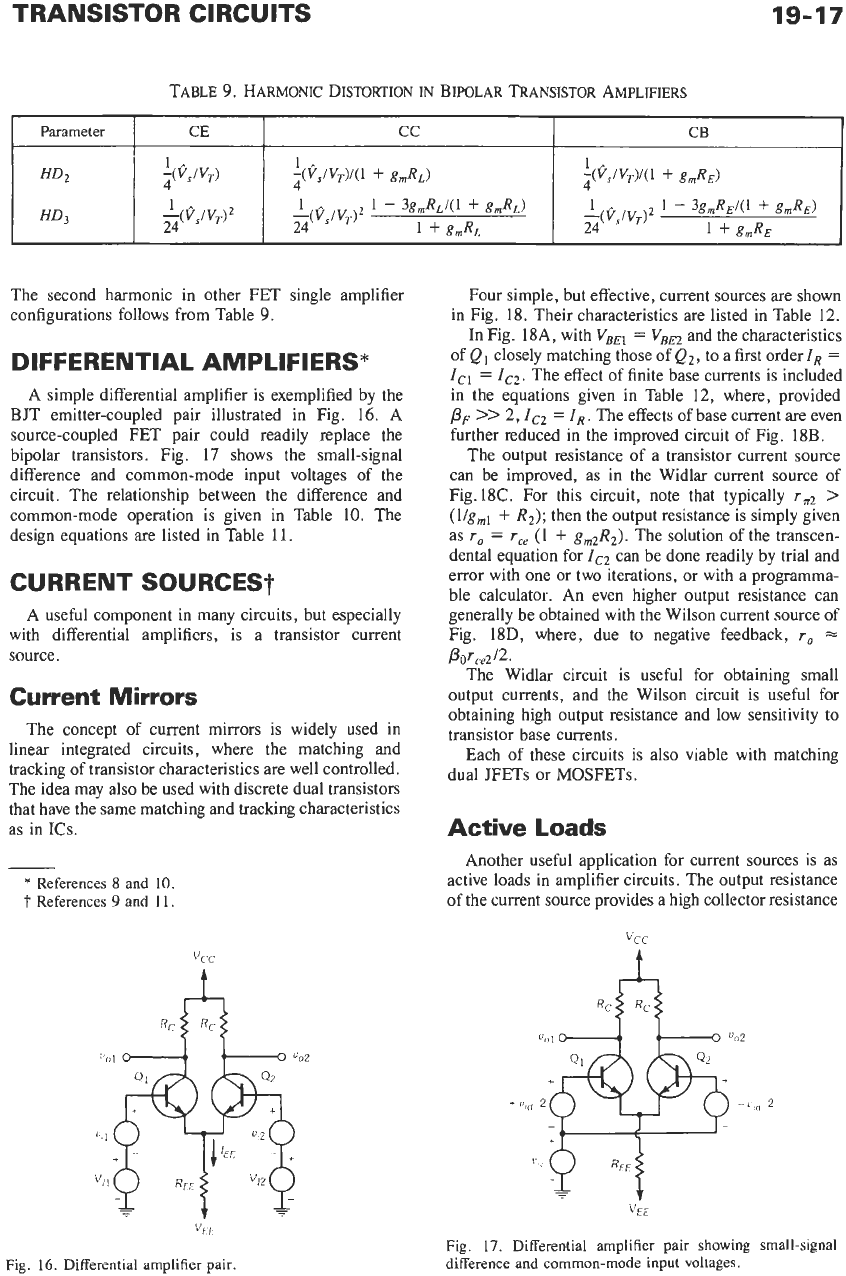
DIFFERENTIAL AMPLIFIERS*
A simple differential amplifier is exemplified by the
BJT emitter-coupled pair illustrated in Fig. 16. A
source-coupled FET pair could readily replace the
bipolar transistors. Fig.
17
shows the small-signal
difference and common-mode input voltages of the
circuit, The relationship between the difference and
common-mode operation is given in Table
10.
The
design equations are listed in Table
11.
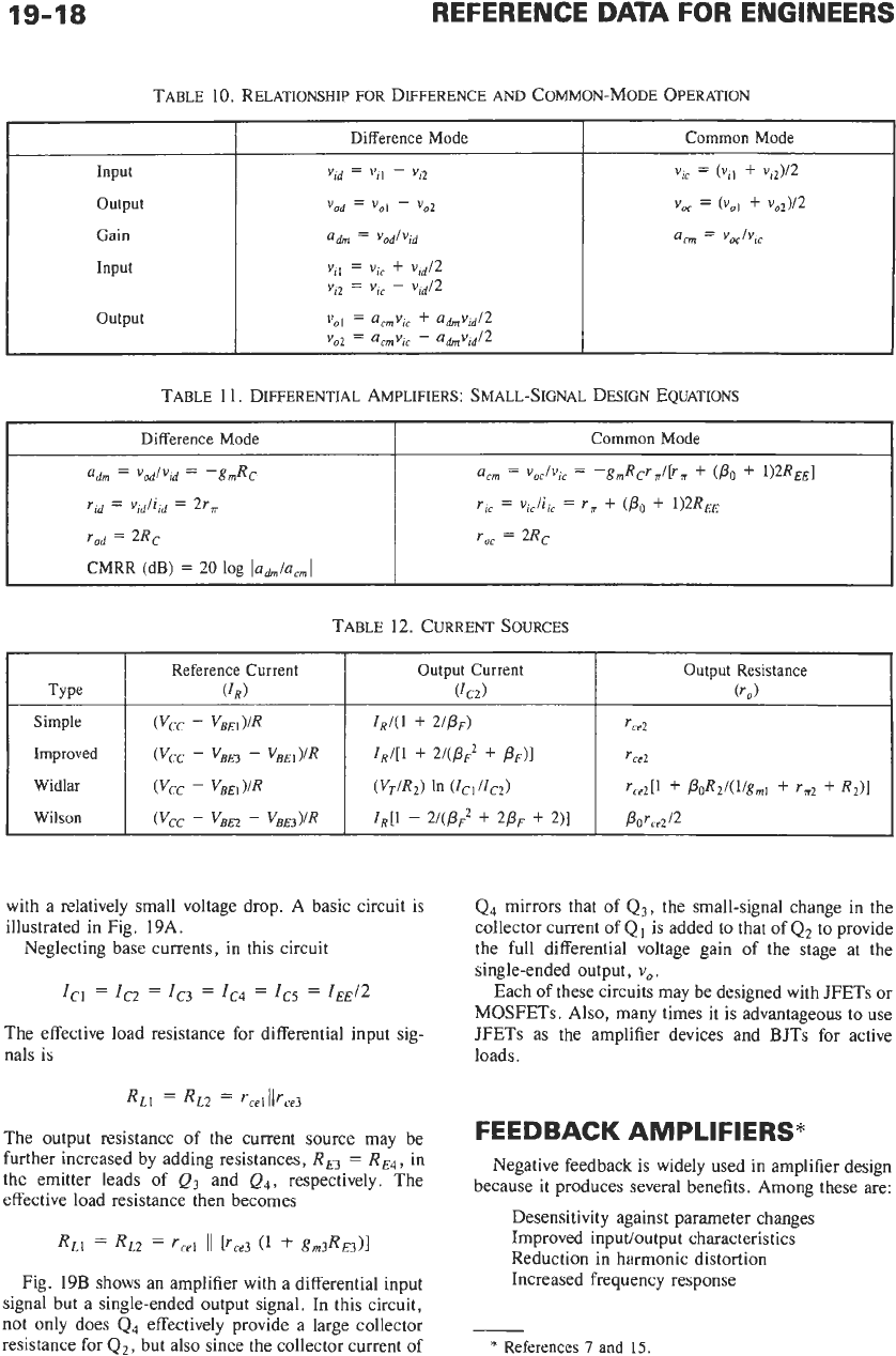
CURRENT SOURCES?
A
useful component in many circuits, but especially
with differential amplifiers, is a transistor current
source.
Current Mirrors
The concept of current mirrors is widely used in
linear integrated circuits, where the matching and
tracking of transistor characteristics are well controlled.
The idea may also be used with discrete dual transistors
that have the same matching and tracking characteristics
as in
ICs.
-
*
References
8
and
10.
T
References
9
and
11.
v,
i
Fig.
16.
Differential amplifier pair.
Four simple, but effective, current sources are shown
in Fig. 18. Their characteristics are listed in Table 12.
In Fig. l8A, with
VBEl
=
VBn
and the characteristics
of
Q
closely matching those
of
Q2,
to a first order
iR
=
IC,
=
Ic2.
The effect of finite base currents is included
in the equations given in Table 12, where, provided
PF
>>
2,
IC2
=
iR.
The effects of base current are even
further reduced in the improved circuit of Fig.
18B.
The output resistance of a transistor current source
can be improved, as in the Widlar current source of
Fig.18C. For this circuit, note that typically
rrr2
>
(l/gml
+
R2); then the output resistance is simply given
as
ro
=
rce
(1
+
gm2R2).
The solution of the transcen-
dental equation for
Ic2
can be done readily by trial and
error with one or two iterations, or with a programma-
ble calculator. An even higher output resistance can
generally be obtained with the Wilson current source of
Fig.
18D,
where, due to negative feedback, r,
=
The Widlar circuit is useful for obtaining small
output currents, and the Wilson circuit is useful for
obtaining high output resistance and low sensitivity to
transistor base currents.
Each of these circuits is also viable with matching
dual JFETs or MOSFETs.
P0rce212.
Active Loads
Another useful application for current sources is as
active loads in amplifier circuits. The output resistance
of the current source provides a high collector resistance
VEi
Fig.
17.
Differential amplifier pair showing small-signal
difference and common-mode input voltages.
19-18
Reference Current Output Current
Type
(IR)
VC2)
REFERENCE
DATA
FOR
ENGINEERS
Output Resistance
(To)
TABLE
10.
RELATIONSHIP
FOR
DIFFERENCE
AND
COMMON-MODE OPERATION
Input
output
Gain
Input
output
Difference Mode
Common Mode
TABLE
1
1.
DIFFERENTIAL AMPLIFIERS: SMALL-SIGNAL DESIGN EQUATIONS
I
Difference Mode
I
Common Mode
I
with a relatively small voltage drop.
A
basic circuit is
illustrated in Fig. 19A.
Neglecting base currents, in this circuit
IC1
=
IC2
=
IC3
=
IC4
=
ICs
=
IEE/2
The effective load resistance for differential input sig-
nals is
The output resistance
of
the current source may be
further increased by adding resistances,
RE3
=
RE4,
in
the emitter leads
of
Q3
and
Q4,
respectively. The
effective load resistance then becomes
Fig. 19B shows an amplifier with a differential input
signal but a single-ended output signal. In this circuit,
not
only
does
Q4
effectively provide a large collector
resistance for
Q2,
but
also
since the collector current of
Q4
mirrors that of
Q3,
the small-signal change in the
collector current
of
Q1
is added to that of
Q2
to provide
the full differential voltage gain of the stage at the
single-ended output,
v,.
Each of these circuits may be designed with JFETs or
MOSFETs. Also, many times it is advantageous to use
JFETs as the amplifier devices and
BJTs
for active
loads.
FEEDBACK
AMPLIFIERS*
Negative feedback is widely used in amplifier design
because it produces several benefits. Among these are:
Desensitivity against parameter changes
Improved input/output characteristics
Reduction in harmonic distortion
Increased frequency response
-
*
References
7
and
15.
TRANSISTOR CIRCUITS
19-19
"CC
+V
(A)
Simple
"CC
Qi
-
-
Unfortunately there are some disadvantages:
Reduced gain
Instability problems
Basic
Properties
The basic properties of negative feedback are pre-
sented with the aid
of
the block diagram in Fig.
20.
In
this diagram, the gain
of
the basic amplifier,
a,
is
controlled by undependable transistor parameters that
are subject to considerable variation. It is assumed that
gain
a
is much larger than needed. It is also assumed in
the block diagram that there is no loading
of
one block
by another block and the signal path is only in the
direction of the arrows;
Le.,
the gain
of
each block is
unilateral.
vcc
t
(E)
Improved.
"CC
(A)
Dlfferenrlal amplifier
palr
wlth
actlue load
&
(C)
Widlor.
"CC
'c2
Q3
-
-
(0)
Wilson.
Fig.
18.
Current-mirror circuits.
+
"EE
(E)
Modlfied
octiue
load
for
dinerentin1 amplifier palr
Fig,
19.
Active
loads.