Middleton W.M. (ed.) Reference Data for Engineers: Radio, Electronics, Computer and Communications
Подождите немного. Документ загружается.

19-20
REFERENCE
DATA
FOR ENGINEERS
With
positive feedback:
si
=
s,
+
Sf
That is, the signals
add
and
si
>
s,.
With
negative feedback:
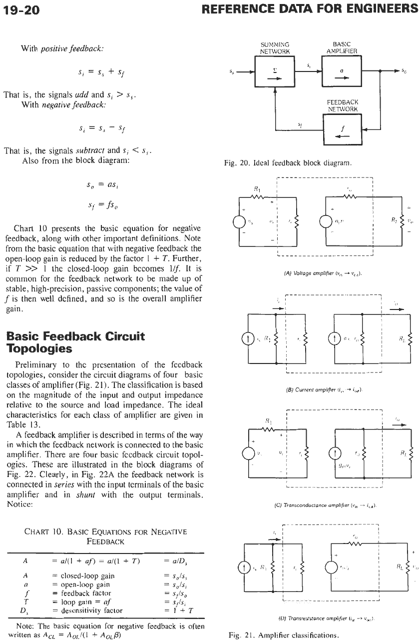
SUMMING
BASIC
NETWORK AMPLIFIER
FEEDBACK
NETWORK
si
=
s,
-
Sf
That is, the signals
subtract
and
si
<
s,.
Also from the block diagram:
Chart 10 presents the basic equation for negative
feedback, along with other important definitions. Note
from the basic equation that with negative feedback the
open-loop gain is reduced by the factor
1
+
T.
Further,
if
7
>>
1 the closed-loop gain becomes
lg.
It is
common for the feedback network to be made up of
stable, high-precision, passive components; the value
of
f
is then well defined, and
so
is the overall amplifier
gain.
Basic Feedback Circuit
Topologies
Preliminary to the presentation of the feedback
topologies, consider the circuit diagrams of four basic
classes
of
amplifier (Fig.
21).
The classification is based
on
the magnitude of the input and output impedance
relative
to
the source and load impedance. The ideal
characteristics for each class of amplifier are given in
Table
13.
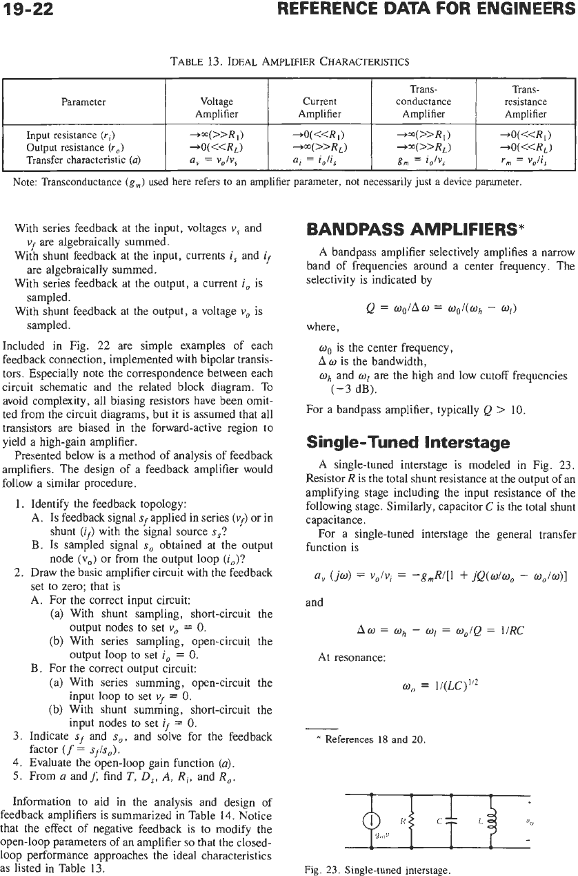
A feedback amplifier is described in terms of the way
in which the feedback network is connected to the basic
amplifier. There are four basic feedback circuit topol-
ogies. These are illustrated in the block diagrams of
Fig. 22. Clearly, in Fig. 22A the feedback network is
connected in
series
with the input terminals of the basic
amplifier and in
shunt
with the output terminals.
Notice:
CHART
10.
BASIC
EQUATIONS
FOR
NEGATIVE
FEEDBACK
A
=
u/(l
+
uf)
=
u/(l
+
T)
=
ulD,
A
=
closed-loop gain
=
soh,
f
=
feedback factor
=
srIso
T
=
loop gain
=
af
=
S,/S,
a
=
open-loop gain
=
soh,
D,
=
desensitivity factor
=1+T
Note:
The basic equation for negative feedback is often
written as
A,
=
AoL/(l
+
AoLP)
Fig.
20.
Ideal feedback block diagram.
,____________________--
I I
r,n
I
I
'I
j
I
'k
+I
!-
+qg
I
I
I
I
(E)
Current
amplifier (i,"
-
zOuJ
(C)
Transconductonce
urnpllfier
(v,"
+
r,,,)
(0)
Transreslstance
arnpiifler
(t,"
--*
vQUJ
Fig.
21.
Amplifier classifications.
TRANSISTOR CIRCUITS
19-21
SUMMlNG BASIC
NETWORK AMPLIFIER
+
RI
r-----i
+
I
I
I
I
5
I
u,
a,=u,/ui
I
I
L-----J
-
I* ?I
-
+
-
"1
I=Uf/uo
-
FEEDBACK
NETWORK
(A)
Serles-shunt feedback configuratlon
'E)
Shunt-series feedback configuratlon
(a
current ampllfler).
(C)
Series-series feedback
-~
_________~
configuration
(a
transconductance
arnpilfier)
r-----i
+
""
-
+
"0
-
(D)
Shunt-shunt feedback configuration
(a
transreslstonce arnpllfier)
Fig,
22. Feedback-amplifier
topologies.
19-22
Voltage
Amplifier
REFERENCE DATA FOR ENGINEERS
Trans- Trans-
Current conductance
resistance
Amplifier Amplifier Amplifier
TABLE 13. IDEAL AMPLIFIER CHARACTERISTICS
Input resistance
(ri)
Output resistance
(To)
Transfer characteristic
(a)
Parameter
+m(
>>R,
)
+O(<<R,)
+q
>>R
,
)
+O(<<R,)
+O(
<<RL)
+m(>>RL)
+m(>>R,)
+O(
<<I?,)
g,
=
iJvS
r,
=
vJiJ
a,
=
v,/v,
ai
=
iJi,
With series feedback at the input, voltages
v,
and
With shunt feedback at the input, currents
is
and
ij
With series feedback at the output, a current
io
is
With shunt feedback at the output, a voltage
v,
is
vf
are algebraically summed.
are
algebraically summed.
sampled.
sampled.
Included
in
Fig. 22 are simple examples of each
feedback connection, implemented with bipolar transis-
tors. Especially note the correspondence between each
circuit schematic and the related block diagram. To
avoid complexity, all biasing resistors have been omit-
ted from the circuit diagrams, but it
is
assumed that all
transistors are biased in the forward-active region to
yield a high-gain amplifier.
Presented below is a method of analysis of feedback
amplifiers. The design of a feedback amplifier would
follow a similar procedure.
1.
Identify the feedback topology:
A. Is feedback signal
sf
applied in series
(vf)
or in
shunt
(if)
with the signal source
s,?
B.
Is
sampled signal
so
obtained at the output
node (v,) or from the output loop
(io)?
2.
Draw the basic amplifier circuit with the feedback
set to zero; that is
A. For the correct input circuit:
(a) With shunt sampling, short-circuit the
(b) With series sampling, open-circuit the
output nodes to set
v,
=
0.
output loop to set
io
=
0.
B. For the correct output circuit:
(a) With series summing, open-circuit the
(b) With shunt summing, short-circuit the
3.
Indicate
sj
and
so,
and solve for the feedback
4.
Evaluate the open-loop gain function
(a).
5.
From
a
and5 find
T,
D,,
A,
Ri,
and
R,.
Information to aid in the analysis and design of
feedback amplifiers is summarized in Table
14.
Notice
that the effect of negative feedback is to modify the
open-loop parameters of an amplifier
so
that the closed-
loop performance approaches the ideal characteristics
as listed in Table 13.
input
loop
to set
vf
=
0.
input nodes to set
if
=
0.
factor
(f
=
sf/so).
BANDPASS AMPLIFIERS*
A bandpass amplifier selectively amplifies a narrow
band of frequencies around a center frequency. The
selectivity is indicated by
Q
=
OolAw
=
Wo/(Wh
-
Wr)
where,
wo
is the center frequency,
A
w
is the bandwidth,
and
w!
are the high and low cutoff frequencies
(-3
dB).
For a bandpass amplifier, typically
Q
>
10.
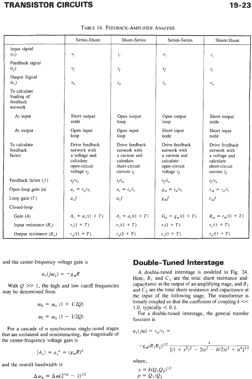
Single-Tuned lnterstage
A single-tuned interstage is modeled in Fig. 23.
Resistor
R
is the total shunt resistance at the output of an
amplifying stage including the input resistance of the
following stage. Similarly, capacitor
C
is the total shunt
capacitance.
For a single-tuned interstage the general transfer
function is
a,
(jo)
=
vo/vi
=
-g,R/[l
+
jQ(w/w,
-
o,/w)]
and
At resonance:
w,
=
l/(LC)l’*
*
References
18 and
20.
Fig.
23.
Single-tuned interstage.
TRANS
I
STO
R
CI
RCU ITS
19-23
TABLE
14.
FEEDBACK-AMPLIFIER ANALYSIS
Input signal
Feedback signal
Output Signal
To
calculate
loading
of
feedback
network
(Si)
(Sf)
(so)
At input
At output
To
calculate
feedback
factor
Feedback factor
(f)
Open-loop gain
(a)
Loop gain
(T)
Closed-loop
Gain
(A)
Input resistance
(R,)
Output resistance
(R,)
Series-Shunt
Short
output
node
Open input
Drive feedback
network with
a voltage and
calculate
open-circuit
voltage
vf
loop
Vf/VO
a
"f
a,
=
vo/vi
A,
=
u,,/(l
+
T)
rj(l
+
T)
ro/(l
+
T)
S
hunt-Series
Open output
Open input
Drive feedback
network with
a current and
calculate
short-circuit
current
if
i+i0
loop
loop
a.
=
i
/i.
a
if
I
01
Ai
=
ai/(l
+
T)
ri/(l
+
T)
r,(l
+
T)
and the center-frequency voltage gain is
a,(jW,)
=
-g,R
With
Q
>>
1, the high and low cutoff frequencies
may be determined from
=
W,
(1
+
1/2Q)
01
=
W,
(1
-
1/2Q)
For a cascade of
n
synchronous single-tuned stages
that
are
unilateral and noninteracting, the magnitude of
the center-frequency voltage gain
is
and the overall bandwidth is
Series-Series
Open output
Short input
node
Drive feedback
network with
a current and
calculate
open-circuit
voltage
vr
vf/i,
g,
=
i0hi
loop
gmf
G,
=
g,/(l
+
T)
ri(l
+
T)
r,(l
+
T)
Shunt-Shunt
Short output
node
Short input
node
Drive feedback
network with
a
voltage and
calculate
short-circuit
current
if
if/vo
r,
=
vo/ii
rmf
R,
=
r,/(l
+
T)
ri/(l
+
T)
rJ1
+
T)
Double-Tuned
lnterstage
A
double-tuned interstage
is
modeled in Fig.
24.
Here,
R,
and
CI
are
the total shunt resistance and-
capacitance at the output of an amplifying stage, and
R2
and
C2 are
the total shunt resistance and capacitance at
the input of the following stage. The transformer is
loosely coupled
so
that the coefficient of coupling
k
<<
1.0,
typically
<
0.1.
For a double-tuned interstage, the general transfer
function
is
U,(jW)
=
V,/Vi
=
where,
A@,,
=
Aw(2""
-
1)'"
19-24
REFERENCE
DATA
FOR ENGINEERS
Fig.
24.
Double-tuned interstage.
b
=
(Qi/Q2
+
Q~/QI)
a
=
(Q1Q2)1’2
(o/wo
-
wo/o)
At resonance:
The gain
of
the interstage is at a maximum with
s
=
1;
the transformer is then critically coupled, and
a,(joo)
=
-g,(R1R2)i’2/2
with
k,
=
WQIQ~”~
In
practice, it is customary to use not the value of
k
which gives the maximum gain, but that value which
gives the Rattest selectivity curve. The circuit is then
said to be transitionally coupled.
k,
=
[(1/Qi2
+
1/Q;)/2]”2
For a transitionally coupled circuit
a,(jwo)
=
-g,(R1Rz)i’2[2p(l
+
p2)]112/(l
+
p)’
and the bandwidth is
Aw
=
[(l
+
p)/~p]
wO/&
With equal
Q’s,
Q,
=
Q2
=
Q,, it follows that
k,
=
k,
=
k,
and
a,(jwo)
=
-g,(RIR2)’12/2
Aw
=
~ wo/Q,
and
k,
=
Aw/-\/2
oo
=
l/Q,
Comparing a double-tuned interstage (with
n
=
1)
and a single-tuned interstage yields the same center-
frequency gain, but the double-tuned circuit provides a
squarer response over the passband.
For a cascade of
n
synchronous double-tuned stages
that are unilateral and noninteracting, the magnitude of
the center-frequency voltage gain is
\A,\
=
a:
=
[g,(R,R2)”2/2]”
and the overall bandwidth is
Awn
=
h~(2”~
-
“cc
t
(A)
Bipolar
junction
tronslstor.
(B)
Junction
fleld-effect
transistor.
Fig.
25.
Transformer-coupled feedback oscillators.
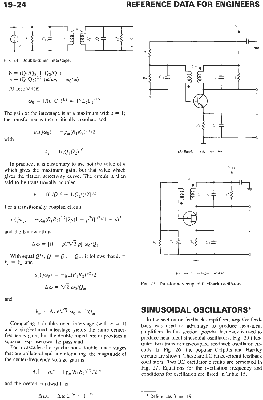
SINUSOIDAL OSCILLATORS*
In
the section
on
feedback amplifiers,
negative
feed-
back was used to advantage
to
produce near-ideal
amplifiers.
In
this section,
positive
feedback is used to
produce near-ideal sinusoidal oscillators. Fig. 25 illus-
trates two transformer-coupled feedback oscillator cir-
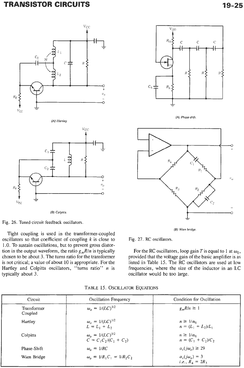
cuits. In Fig. 26, the popular Colpitts and Hartley
circuits are shown. These are LC tuned-circuit feedback
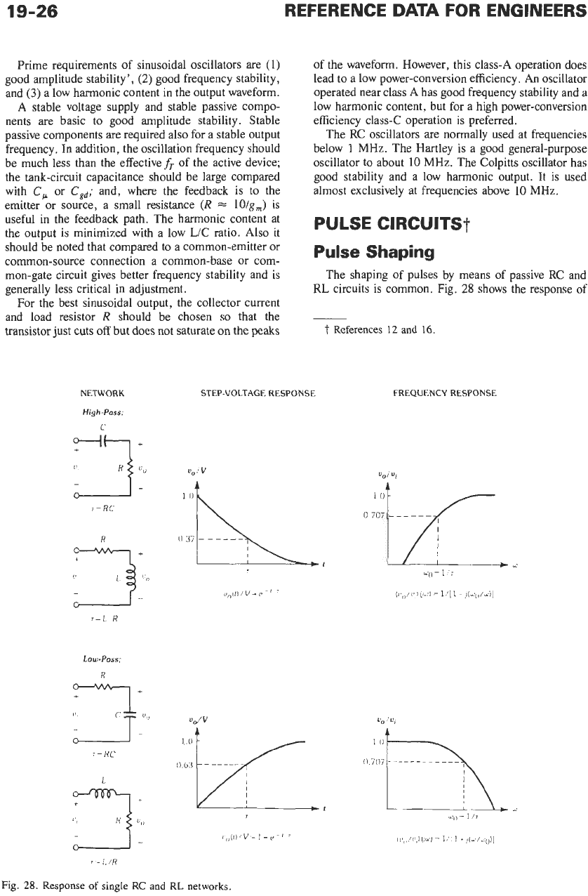
oscillators. Two
RC
oscillator circuits are presented in
Fig.
27.
Equations for the oscillation frequency and
conditions for oscillation are listed in Table
15.
-
*
References
3
and
19.
TRANSISTOR
CIRCUITS
Circuit Oscillation Frequency
Transformer
0,
=
l/(LC)”2
Coupled
Hartley
Oo
=
l/(LC)”Z
Colpitts
0,
=
l/(LC)”Z
Phase-Shift
L=L1
+Lz
c
=
C1C2/(C1
+
C,)
w,
=
URC
19-25
Condition
for
Oscillation
g,R/n
2
1
n
2
lis,
n
=
(L,
+
L2)/Ll
n
2
1/a0
n
=
(C,
+
C,)IC,
a,(jo,)
2
29
vcc
t
Wien Bridge
(A)
Hartley
0,
=
l/RICI
=
liRzC2
a,(jo,)
=
3
i.e.,
R,
=
2R,
(A)
Phase-shlft.
I I
(6)
Colpllts
Fig.
26.
Tuned-circuit feedback oscillators.
Tight coupling
is
used in the transformer-coupled
oscillators
so
that coefficient
of
coupling
k
is
close to
1
.O.
To
sustain oscillations, but to prevent gross distor-
tion in the output waveform, the ratio
g,Rh
is typically
chosen to be about
3.
The turns ratio for the transformer
is
not critical; a value of about
10
is appropriate. For the
Hartley and Colpitts oscillators, “turns ratio”
n
is
typically about
3.
(6)
Wlen
brldge
Fig.
27.
RC oscillators.
For the RC oscillators, loop gain
T
is equal to
1
at
wo
,
provided that the voltage gain of the basic amplifier is as
listed in Table
15.
The RC oscillators are used at low
frequencies, where the size of the inductor in an LC
oscillator would be too large.
19-26
REFERENCE DATA
FOR
ENGINEERS
Prime requirements of sinusoidal oscillators are
(1)
good amplitude stability',
(2)
good frequency stability,
and
(3)
a low harmonic content in the output waveform.
A stable voltage supply and stable passive compo-
nents are basic to good amplitude stability. Stable
passive components are required also for a stable output
frequency. In addition, the oscillation frequency should
be much less than the effective& of the active device;
the tank-circuit capacitance should be large compared
with
C,
or
Cgd;
and, where the feedback is to the
emitter or source, a small resistance
(R
=
lO/g,)
is
useful in the feedback path. The harmonic content at
the output is minimized with a low
L/C
ratio.
Also
it
should be noted that compared to a common-emitter or
common-source connection a common-base or com-
mon-gate circuit gives better frequency stability and is
generally less critical in adjustment.
For the best sinusoidal output, the collector current
and load resistor
R
should be chosen
so
that the
transistor just cuts off but does not saturate on the
peaks
of the waveform. However, this class-A operation does
lead to a low power-conversion efficiency. An oscillator
operated near class
A
has good frequency stability and a
low harmonic content, but for a high power-conversion
efficiency class-C operation is preferred.
The
RC
oscillators are normally used at frequencies
below
1
MHz. The Hartley is a good general-purpose
oscillator to about
10
MHz. The Colpitts oscillator has
good stability and a low harmonic output.
It
is used
almost exclusively at frequencies above
10
MHz.
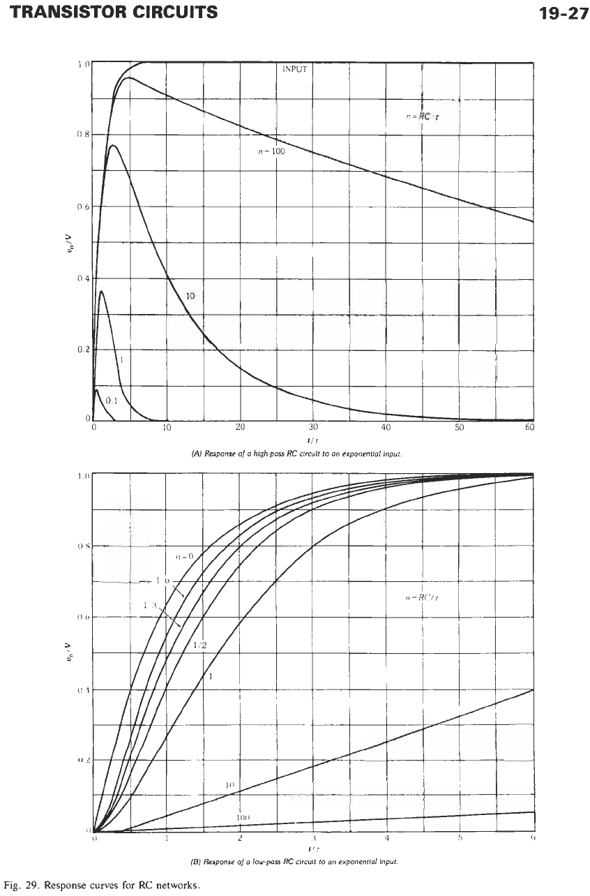
PULSE CIRCUITST
Pulse
Shaping
The shaping of pulses by means of passive
RC
and
RL
circuits is common. Fig.
28
shows the response of
NETWORK
STEP-VOLTAGE RESPONSE
High-Poss.
U,'V
r=RC
R
Lr+$+ti"
i=L
R
Low-Pass:
R
7'
2
-""
i=RC
L
t
References
12
and
16
FREQUENCY RESPONSE
",/",
Fig.
28.
Response
of
single RC and RL networks.
TRANSISTOR CIRCUITS
19-27
tlr
(A)
Response
of
a
high-pass RC
clrcult
to
an exponential Input.
tli
(E)
Response
of
a
low-pass
RC
circuit
to
an
exponential input
Fig.
29.
Response
curves
for
RC
networks.
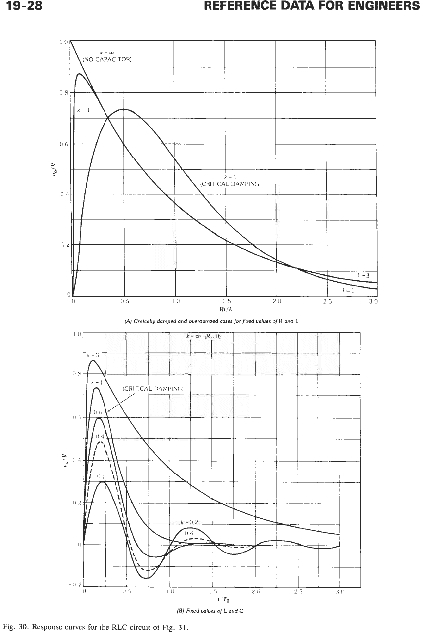
19-28
REFERENCE
DATA
FOR ENGINEERS
01
01
?
0
05
10
15
20
30
RtIL
[A)
Critlcallv
damped and overdamped
cases
for
fixed
vdues
of
R
and
L.
15
'.'To
(E)
Fked
unfues
of
L
ond
C
Fig.
30.
Response
curves
for
the
RLC
circuit
of
Fig.
31.
TRANSISTOR CIRCUITS
19-29
each of these simple networks to a step-voltage input
and a sine-wave input. For a step input,
vi
=
V.
With a
step-voltage at the input of a simple high-pass network,
the fall time between the
0.9
and
0.1
points on the
output waveform is
tf
=
2.27.
Similarly, for a simple
low-pass network the rise time between the
0.1
and
0.9
points of the output waveform
is
t,
=
2.27.
The
high-pass network also serves as a voltage differentiator,
since
vu
(t)
=
7(dvi/dt).
The low-pass network serves as
a voltage integrator, since
vu
(t)
=
(UT)
vi&.
The
response of these shaping networks to an exponential
voltage input,
vi
=
V(l
-
e-'"),
is illustrated in Fig.
29.
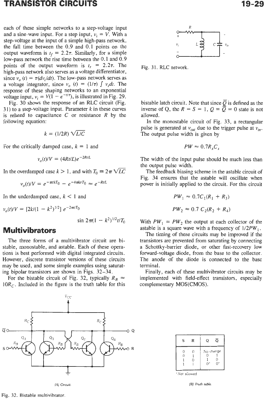
Fig.
30
shows the response of an RLC circuit (Fig.
31)
to a step-voltage input. Parameter
k
in these curves
is, related to capacitance
C
or
resistance
R
by the
following equation:
k
=
(1/2R)
For the critically damped case,
k
=
1
and
v,(t)/V
=
(4Rt/15)e-~~~'~
In the overdamped case
k
>
1,
and with
To
E
257
a
v,(tyv
=
e-l"/kTo
-
e-4rrkt/To
e-Rt/L
In the underdamped case,
k
<
1
and
v,(t)/V
=
[2k/(l
-
k2)"2]
e-21"iT0
sin
2?r(l
-
k2)"2t/T,,
Multivi brators
The three forms of a multivibrator circuit
are
bi-
stable, monostable, and astable. Each of these opera-
tions is best performed with digital integrated circuits.
However, discrete transistor versions of these circuits
may be used, and some simple examples using saturat-
ing bipolar transistors are shown in Figs.
32-34.
For the bistable circuit of Fig.
32,
typically
R,
=
lOR,.
Included in the figure is the truth table for this
R
Fig.
31.
RLC
network.
bistable latch circuit. Note that since
e
is defined as the
inverse of Q, the
R
=
S
=
1,
Q
=
e
=
0
state is not
allowed.
In the monostable circuit of Fig.
33,
a rectangular
pulse
is
generated at
v,,,
due to the trigger pulse at
vin.
The output pulse width is given by
PW
=
O.7RxC,
The width of the input pulse should be much less than
the output pulse width.
The feedback biasing scheme in the astable circuit
of
Fig.
34
ensures that the astable will oscillate when
power is initially applied to the circuit. For this circuit
PWI
=
0.7C1(R,
+
R3)
PW2
=
0.7
C2(R2
+
R4)
With
PW1
=
PW2
the output at each collector of the
astable is a square wave with a frequency of
1/2PW1.
The timing of these circuits may be improved if the
transistors are prevented from saturating by connecting
a Schottky-barrier diode, or other fast-recovery low
forward-voltage diode, from the base to the collector.
The anode of the diode is connected to the base
terminal.
Finally, each
of
these multivibrator circuits may be
implemented with field-effect transistors, especially
complementary MOS(CM0S).
'Not
aiiowed
(B)
Truth
table.
(AJ
Circuit.
Fig.
32.
Bistable multivibrator