Middleton W.M. (ed.) Reference Data for Engineers: Radio, Electronics, Computer and Communications
Подождите немного. Документ загружается.

19-30
REFERENCE
DATA
FOR ENGINEERS
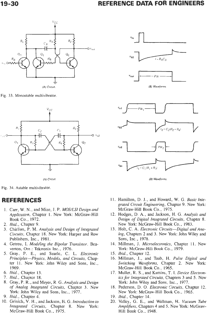
(A)
Circuli.
Fig.
33.
Monostable multivibrator.
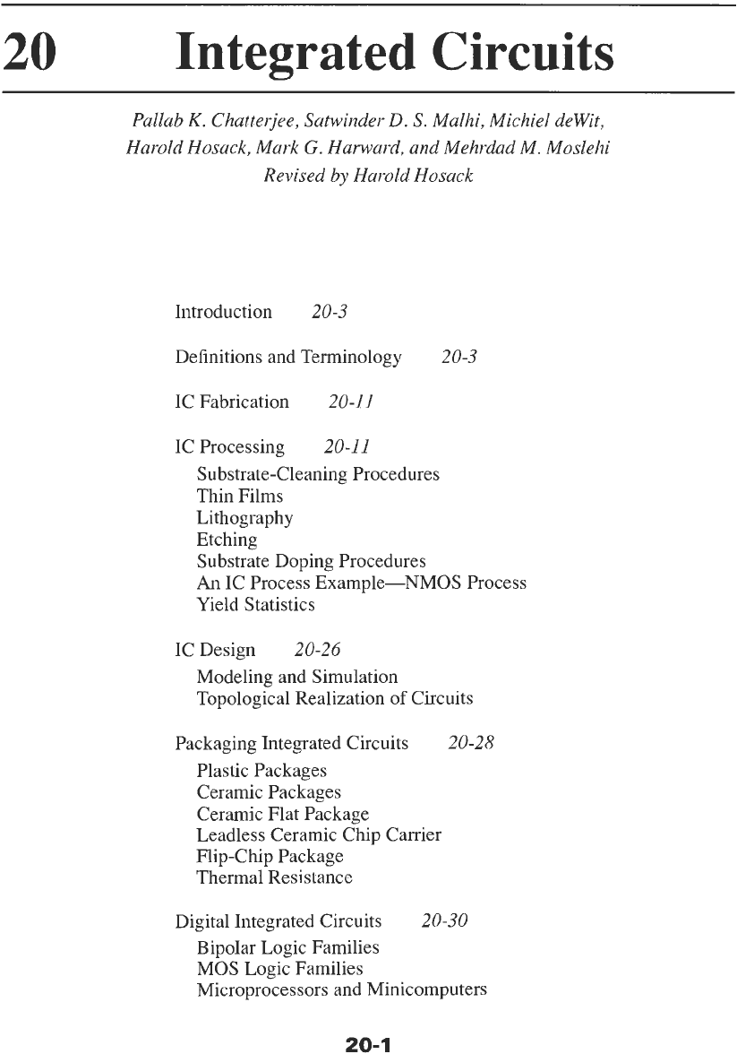
(A)
Circuit
Fig.
34.
Astable multivibrator.
REFERENCES
1.
Cam, W. N., and Mize, J.
P.
MOSILSI Design and
Application,
Chapter 1. New York: McGraw-Hill
Book Co., 1972.
2.
Ibid.,
Chapter 9.
3. Chirlian,
P.
M.
Analysis and Design
of
Integrated
Circuits,
Chapter 18. New York: Harper and Row
Publishers, Inc., 1981.
4.
Getreu,
I.
Modeling the Bipolar Transistor.
Bea-
verton, Ore.: Tektronix
Inc.,
1976.
5.
Gray,
P.
E.,
and Searle,
C. L.
Electronic
Principles-Physics, Models, and Circuits,
Chap-
ter 11. New York: John Wiley and
Sons,
Inc.,
1969.
6.
Ibid.,
Chapter
13.
7.
Ibid.,
Chapter 18.
8.
Gray,
P.
R., and Meyer, R. G.
Analysis and Design
of
Analog Integrated Circuits,
Chapter 3. New
York: John Wiley and Sons,
Inc.,
1977.
9.
Ibid.,
Chapter 4.
lC. Grinich, V. H., and Jackson, H. G.
Introduction to
Integrated Circuits,
Chapter
8.
New York:
McGraw-Hill Book Co., 1975.
"b2
(E)
Waueforms
11. Hamilton,
D.
J., and Howard, W. G.
Basic Inte-
grated Circuit Engineering,
Chapter 9. New York:
McGraw-Hill Book Co., 1975.
12. Hodges,
D.
A.,
and Jackson, H. G.
Analysis and
Design
of
Digital Integrated Circuits,
Chapter
8.
New York: McGraw-Hill Book Co., 1983.
13. Holt, C.
A.
Electronic Circuits-Digital and Ana-
log,
Chapters 2 and 3. New York: John Wiley and
Sons, Inc., 1978.
14. Millman, J.
Microelectronics,
Chapter 11. New
York: McGraw-Hill
Book
Co., 1979.
15.
Ibid.,
Chapter 12.
16. Millman, J., and Taub,
H.
Pulse Digital and
Switching Waveforms,
Chapter 2. New York:
McGraw-Hill Book Co., 1965.
17. Muller, R.
S.,
and Kamins, T.
I.
Device Electron-
ics for Integrated Circuits,
Chapters 3 and
5.
New
York: John Wiley and
Sons,
Inc., 1977.
18. Pederson,
D.
0.
Electronic Circuits,
Chapter 12.
New York: McGraw-Hill
Book
Co., 1965.
19.
Ibid.,
Chapter 14.
20. Valley, G.
E.,
and Wallman, H.
Vacuum Tube
Amplijiers,
Chapters
4
and
5.
New York: McGraw-
Hill Book Co., 1948.
20
Integrated Circuits
Pallab
K.
Chatterjee, Satwinder
D.
S.
Malhi, Michiel deWit,
Harold Hosack, Mark
G.
Harward, and Mehrdad
M.
Moslehi
Revised by Harold Hosack
Introduction
20-3
Definitions and Terminology
20-3
IC Fabrication
20-11
IC Processing
20-11
Substrate-Cleaning Procedures
Thin Films
Lithography
Etching
Substrate Doping Procedures
An
IC Process Example-NMOS Process
Yield Statistics
IC Design
20-26
Modeling and Simulation
Topological Realization
of
Circuits
Packaging Integrated Circuits
20-28
Plastic Packages
Ceramic Packages
Ceramic Flat Package
Leadless Ceramic Chip Carrier
Flip-Chip Package
Thermal Resistance
Digital Integrated Circuits
20-30
Bipolar Logic Families
MOS Logic Families
Microprocessors and Minicomputers
20-1
20-2
REFERENCE
DATA
FOR ENGINEERS
Memory Integrated Circuits
20-39
Read-only Memories (ROM)
Nonvolatile Read-only Memories
Random-Access Memories (RAM)
New Developments
Linear Integrated Circuits
20-42
Differential Amplifier
Operational Voltage Amplifier
Other Amplifiers
Voltage Reference
Voltage Regulators
Comparators
Special-Purpose Linear Integrated Circuits
Miscellaneous Linear ICs
Trends in Integrated Circuits
20-45
Scaling and Miniaturization
Image-Sensing ICs
Speech-Synthesizer IC
System in a Package (SIP) and System on a Chip (SOC)
Micro-Electro-Mechanical
Systems (MEMS)
Application Specific Integrated Circuits
20-49
Gate Arrays
Future Trends in ASICs
Single-Wafer Integrated Device Processing
20-56
Single-Wafer Semiconductor Manufacturing
Integrated Device Manufacturing
RTP for Integrated Device Processing
Single-Wafer Surface Cleaning
Single-Wafer Epitaxy
Single-Wafer Plasma Processing
SWP-Based Process and Device Integration
Silicon-on-Insulator Technology
and
Devices
SO1 Material Options
Device Structures Using
SO1
Materials
Devices
on
SO1
Nonfully Depleted Devices
Fully Depleted Devices
SO1 Circuits
Three-Dimensional ICs
Conclusion
20-1
02
INTRODUCTION
Progress in the complexity and usefulness of inte-
grated circuits (ICs) has been extremely rapid over the
past four decades.
In
fact, the pace of introduction of
new ICs and new IC applications has continued to
increase over this time. Currently ICs are a pervasive
element in essentially all parts of commercial, scien-
tific, and military systems. They have allowed major
advances in such areas as computers, entertainment
electronics, video cameras, global positioning systems,
and innumerable other applications. The impact
of
ICs
on
society in
the
past forty years has been comparable
to the impact
of
the industrial revolution. The rapid
rate of change experienced during the recent past is
expected to continue well into the next millennium.
This chapter describes some
of
the basic concepts of
integrated circuits, integrated circuit fabrication,
designs, and a few applications.
DEFINITIONS AND
TERMINOLOGY
access time:
1.
Address-to-read output access
time-The time delay in random-access memo-
ries from the application of appropriate address
signal levels to the presence of valid data signal
levels at the output. The signal to enable the
memory chip enable is present.
2.
Chip-enable-
to-read output access time-With an appropriate
address signal level present, the time delay in
random-access memories from the application
of appropriate signal levels to the enable inputs
to the presence of valid data signal levels at the
output.
adder:
Switching circuit that combines binary bits
to generate the sum and carry of these bits. Takes
the bits from two binary numbers to be added
(addend and augend), plus the carry from
the
pre-
ceding less-significant bit, and generates the sum
and carry.
APCVD:
Atmospheric pressure chemical vapor dep-
osition.
ARC:
Antireflection coating used in resist process-
ash:
Isotropic
dry
etching of resist with
0,.
avalanche breakdown:
Reverse-voltage breakdown
due to electrons gaining sufficient speed to dis-
lodge valence electrons and thus create more cur-
rent carriers.
backgrind:
Process
of
removal of material from
ball bond:
Connecting wire from package to IC chip.
barrier layer:
A thin layer deposited
on
contacts
before metallization that prevents metal spikes
ing.
back side of wafers by grinding.
from penetrating through thin junctions and caus-
ing unwanted shorts.
beta ratio:
For
all
standard p-channel and n-channel
MOS
structures, the coefficient
(pOx)/(2t0,)
for the
driver device is equal to that of the load device.
In
this
equation,
p
=
majority carrier mobility,
E,,
=
permittivity of the oxide, and
tax
=
thickness of the
oxide over
the
channel. Hence, the beta ratio
sim-
ply becomes the ratio of
(W/L)bx,er
to
(WIL),,,,,
where
W
=
width of the channel and
L
=
length of
the channel in the direction of the current. Some
engineers use the symbol
KR
to denote this same
ratio.
bias, forward:
An
external voltage applied in the
conducting direction of a
pn
junction. This is
accomplished by connecting the positive terminal
of the source to the p-type region and the negative
terminal to the n-type region.
bias, reverse:
An
external voltage applied
in
the
nonconducting direction of a pn junction. The
connections are opposite to those for forward
bias.
binary coded decimal
(BCD):
A binary numbering
system for coding decimal numbers in groups of
four bits. The binary value of these four-bit
groups ranges from
0000
to
1001
and codes the
decimal digits
0
through
9.
To
count to
9
takes
four bits; to count to
99
takes two groups of four
bits; to count to
999
takes three groups of four
bits; etc.
binary logic:
Digital logic elements that operate
with two distinct states. The two states
are
vari-
ously called true and false, high and low,
on
and
off,
or
1
and
0.
In
computers they
are
represented
by two different voltage levels. The level that is
more positive (or less negative) than the other is
called the high level; the other is called the low
level. If the true
(1)
level is the most positive volt-
age, such logic
is
referred to as “positive true” or
“positive logic.”
bipolar technology:
Semiconductor fabrication
involving an active semiconductor device with
two or more pn junctions. Conduction is by a flow
of electrons (in n-type material)
or
positive holes
(in p-type material) across the junction of
the
two
materials.
bird beak:
Edge feature produced during local oxi-
dation.
bistable element:
Another name for flip-flop. A cir-
cuit
in
which the output has two stable states (out-
put levels
0
and
1)
and can be caused to go to
either of these states by input signals, but remains
in that state permanently after the input signals are
removed.
This
differentiates
the
bistable element
from a gate, which
also
has two output states but
which requires the retention
of
the input signals to
stay in a given state. The characteristic
of
two sta-
ble states also differentiates the bistable element
from a monostable element, which keeps return-
ing to a specific state, and an astable element,
which keeps changing from one state to the other.
bit:
Binary digit.
boat:
Wafer holder generally made of quartz or pol-
BTS:
Bias temperature stress.
buffer memory:
A
memory system, usually of small
capacity compared to a main-frame memory, that
provides a buffer function between two digital
activities.
ysilicon used during furnace processes.
bus:
Long signal-carrying line.
byte:
Eight bits.
CADICAEICAM:
Computer-aided designfcomputer-
aided
engineeringfcomputer-aided
manufacture.
CDZ:
Collector diffusion isolation.
A
bipolar semi-
conductor fabrication process that uses an epitax-
ial layer for the base structure (eliminating a
base-diffusion step) and combines
the
deep col-
lector diffusion contact and isolation steps.
Cell: A
collection of devices that is repeated in a cir-
cuit. Mostly used to describe unit memory struc-
tures.
character generation:
A
design technique for inte-
grated circuits that utilizes a fixed program in a
storage element as the means for generating a dot
matrix to represent alphanumeric characters on a
CRT display.
charge-coupled device (CCD):
A
type of semicon-
ductor device in which the presence or absence of
charge represents the information. Charge-cou-
pled devices store minority-carrier charges in
potential wells created at the silicon surface and
transport these charge packets along the surface
by moving the potential wells.
chip enable:
The control signal that activates
a
com-
plete storage element.
No
reading or writing of
data occurs unless this signal activates the storage
element.
class
N:
Measure
of
particulate contamination in
clean rooms.
N
particles of size seater than
0.3
,run per cubic foot.
clock: A
timing control signal required by storage
elements and memory systems.
CMOS:
See
complementary
MOS.
C,:
Gate capacitance corresponding to the oxide
layer over the channel area;
C,
=
A(.soxltox).
A
=
channel area,
E,*
=
permittivity of oxide,
tox
=
thickness of oxide over channel.
column decoder:
Circuits within the storage ele-
ments designed
to
route data from a column of
storage cells.
complementary
MOS:
An
MOS
fabrication process
that combines both p-channel and n-channel tran-
sistors on the same substrate. The n-channel tran-
sistor is usually
the
driver device, and the p-
channel transistor is the load. Only one transistor
of the pair is normally on, except during the
switching mode.
cuit.
complexity:
The number of equivalent gates in a cir-
Cu-low
k:
Description
of
advanced IC metallization
that is composed of thin films of copper separated
by a very low dielectric constant medium.
current, forward:
The net current that flows across
the forward-biased pn junction.
CVD:
Chemical vapor deposition of
thin
films.
cycle time:
1.
Read cycle time-The total time
required between the application of address infor-
mation for reading data number
1
and the applica-
tion of address information for reading data
number
2
with the memory in the read mode.
2.
Write cycle time-Same as read cycle time, but
for writing of data and memory
in
the write
mode.
3.
System cycle time-The time between
memory cycle initiations. It usually is determined
by the longest of the read or write access or read
or write cycle times.
using a single crystal seed.
Czochralski:
Crystal-pulling process from a melt
Damascene processing:
Metal application to ICs
using a process where metal is deposited on a sur-
face having grooves where metal is desired, and
then the metal is polished from the wafer, leaving
metal
in
the grooves.
decoder: A
conversion circuit that accepts digital
input information
(in
the memory case, binary
address information) that appears as a small num-
ber of lines and selects and activates one of a
large number of output lines.
weak
HF.
deglaze:
Removal of
thin
layer
of
SiO, by the use of
depletion region:
The region in a semiconductor in
which the mobile-carrier charge density is insuffi-
cient to neutralize the net charge density of the
fixed donor and acceptor ions.
descum:
Anisotropic plasma removal of resist resi-
dues after development.
INTEGRATED CIRCUITS
die-by-die alignment:
Alignment mechanism in
diffusion current:
The current produced when
dcffusion length:
The average distance excess minor-
ity carriers diffuse between injection and recom-
bination.
diode isolation:
A method of producing a high elec-
trical resistance between an integrated-circuit ele-
ment and the substrate by surrounding the
element with a reverse-biased pn junction. The
method is also called junction isolation
(JI).
diode, semiconductor:
A two-electrode semiconduc-
tor device that conducts current more easily in
one direction than in the other.
which each die is aligned separately.
charges move by diffusion.
DIP:
Dual in-line package.
direct mapping:
A design technique, used in virtual
memory design, that determines the way data are
organized and transferred from primary memory
to the buffer memory. Data are mapped directly
as blocks.
dope:
Introduction of different atoms (dopant) in a
dose:
Number of implanted or diffused ions per unit
dot matrix:
A matrix
of
dots that is used to identify
alphanumeric characters.
dRAMlsRAM:
Dynamic (refreshed storage cells),
static
(Vcc
only) RAM.
drift current:
A current that is produced when the
carriers move under the influence of an applied
voltage, i.e., owing to a voltage gradient.
drive-in:
Deeper thermal diffusion of dopants intro-
duced during predeposition.
DSW:
Direct step on wafer for step and repeat pro-
jection optical lithography.
dynamic storage elements:
Storage elements that
contain storage cells that must be refreshed at
appropriate time intervals to prevent the loss of
information content.
EAROM:
Electrically alterable ROM. A fixed-pro-
gram semiconductor storage element whose pro-
gram can be altered by the application of external
electrical or optical means.
semiconductor structure,
Q.
area.
E-beam:
Electron beam (exposes resist to pattern
E,:
Conduction-band energy level.
ECL circuits:
Bipolar emitter-coupled logic; also
masks or wafers).
called current-mode logic circuits.
ECL
storage cell:
A type of bipolar storage cell that
is like the multiple-emitter cell but is used for
ECL interface.
EF:
Fermi energy level.
Eg:
Band-gap energy
=E, -E,.
E,:
Intrinsic energy level; assumed to be at the cen-
ter of the band gap.
electromigration:
Metal line failure due to mass
transport of metal under large dc electric field.
electron-beam lithography:
Use of focused electron
beam to delineate patterns in resist. Commonly
used for mask making.
epitaxial growth:
The deposition of a monocrystal-
line layer of material onto a substrate material
such that the layer thus formed has the same crys-
tal orientation as the substrate.
EPROM, EEPROM:
Electrically programmable,
electrically erasable and programmable ROM.
etch filament:
Thin residue left along steps during
anisotropic dry etching.
etch selectivity:
Ability
of
an etchant to remove layers
of certain material with minimal attack
on
others.
E,,:
Valence-band energy level.
excess minority carriers:
The number of minority
carriers that exceeds the normal equilibrium num-
ber in a semiconductor.
factory-programmed
ROM:
A fixed-program semi-
conductor storage element that has been pro-
grammed at the factory with a unique bit pattern.
failure rate:
The number of components that fail in
a given amount of time, usually expressed as a
percentage per
1000
hours.
fall time:
A measure of the time required for the
out-
put voltage of a circuit to change from a high-
voltage level to a low-voltage level once a level
change has started.
fan-out:
The number of loads connected to the out-
put of a logic stage. (A load normally consists of
the input impedance of a logic circuit.)
fiducial:
Markers
on
reticles for aid in alignment in
projection printers.
filming:
Lifting of resist caused by lack of adhesion.
fixed-program storage (read-only memory or read-
only store):
A special application of random-
access storage
in
which storage is fixed after pro-
gramming.
jlip-flop:
A storage element-a circuit having two
stable states and the capability of changing from
one state to another with the application of
a
con-
trol signal and remaining in that state after
removal of signals.
(See
bistable element.)
pip-flop.
D:
The letter
D
stands for delay.
A
flip-flop
whose output is
a
function of the input that
appeared one pulse earlier; for example, if
a
1
appeared at the input, the output after the next
clock pulse would be
a
1.
pip-flop,
JK:
A flip-flop having two inputs, desig-
nated
J
and
K.
At the application of
a
clock pulse,
a
1
on the
J
input and
a
0
on the
K
input will set
the flip-flop to the
1
state;
a
1
on the
K
input and
a
0
on the
J
input will reset it to the
0
state; and
1
simultaneously on both inputs will cause it to
change state regardless of the previous state.
J
=
0
and
K
=
0
will prevent change.
flip-flop,
RS:
A
flip-flop consisting of two cross-cou-
pled
NAND
gates and having two inputs desig-
nated
R
and
S.
A
1 on the
S
input and
0
on the
R
input will reset (clear) the flip-flop to the
0
state;
1
on the
R
input and
0
on the
S
input will set it to
the
1
state. It is assumed that
0
will never appear
simultaneously at both inputs.
If
both inputs have
1, the flip-flop will stay
as
it was.
A
1
is
consid-
ered nonactivating.
A
similar circuit can be
formed with
NOR
gates.
flip-jlop,
RST:
A flip-flop having three inputs desig-
nated
R,
S,
and
T.
This unit works like the
RS
flip-flop, except that the
T
input is used to cause
the flip-flop to change states.
flip-jop,
T:
A
flip-flop having only one input.
A
pulse appearing on the input will cause the flip-
flop to change states. Used in ripple counters.
float zone:
Crystal growth process by repetitive
melting and slow solidification.
fusible metallization:
Utilization of
a
fusible metal,
such
as
Nichrome, in the fabrication of semicon-
ductor memory circuits. The metal interconnec-
tion is severed by
a
high current to program the
storage element.
gate,
AND:
A
logic circuit
in
which all inputs must
have 1-level signals at
the
input to produce
a
1-
level output (assuming positive logic).
gate,
NAND:
A
logic circuit in which all inputs must
have 1-level signals at the input to produce
a
0-
level output (assuming positive logic).
gate,
NOR:
A
logic circuit in which any one input or
more than one input having
a
1-level signal will
produce
a
0-level output (assuming positive logic).
gate,
OR:
A
logic circuit in which any one input or
more than one input having
a
1-level signal will
produce
a
1-level output (assuming positive logic).
gate,
XOR:
A
logic circuit in which
any
odd number
of inputs having
a
1-level signal will produce
a
1-
level output (assuming positive logic).
glass spray:
Quartz particles generated by friction
of
boat with furnace tube during loading and
unloading.
global alignment:
Alignment mechanism in which
only two geometries per wafer are aligned auto-
matically, assuring requisite alignment of others.
g,:
Transconductance
=
61D/6VG/,
GOI:
Gate oxide integrity against applied voltage.
hillocks:
Protrusions in deposited thin films.
Hilton haze:
Hazy look on thin films caused by
departure from stoichiometry, with appearance
akin to Hilton Hotel symbol.
hold time:
The time that address information and
data information must be maintained after write-
enable to guarantee successful writing of data in
the memory.
hydrophilic:
Surface readily wetted by water.
hydrophobic:
Surface not wetted by water.
IGFET:
Insulated-gate field-effect transistor.
input loading factor
(ILF):
The load that an input
line presents
to
a
driver. It may be expressed
as
a
current, voltage, or impedance.
insulator:
A material in which the outer (valence)
electrons
are
tightly bound
to
the atom and are
not free to move.
No
current can flow when
a
voltage less than breakdown is applied across the
material.
integrated circuit:
“The physical realization of
a
number of electrical elements inseparably associ-
ated on or within
a
continuous body of semicon-
ductor material to perform the functions of
a
circuit.”
(EL4
definition)
intrinsic concentration:
The number of free elec-
trons
(or holes) per cubic centimeter
in
an
undoped semiconductor at thermal equilibrium.
ion-beam lithography:
Use of focused ion beams for
pattern delineation.
ion implantation:
An
MOS semiconductor fabrica-
tion process often used to adjust threshold voltage
values by implantation
of
dopant ions in the gate
region, after source and drain formation. The
implanted doping level is controlled by the ion
accelerator beam current and implant time.
ion milling:
Micromachining of
thin
films using
mechanical motion of energetic ions.
isoplanar:
A
bipolar semiconductor fabrication pro-
cess in which the p-diffused isolation regions are
replaced by selectively grown oxide isolation.
junction avalanche: Utilization of an avalanche
junction in the fabrication of fixed-program
(read-only) semiconductor circuits. The ava-
lanched junction forms a connection by high volt-
age and current to program the storage element.
junction barrier: The opposition to the diffusion of
majority carriers across a pn junction caused by
the charge of fixed donor and acceptor ions.
junction capacitor:
A
capacitor utilizing the capaci-
tance of a reverse-biased pn junction.
junction transistor:
An
active semiconductor device
with a base electrode and two or more junction
electrodes.
KOOI
effect: Inhibition of subsequent oxidation of
silicon underlying Si,N, caused by
NH,
formed
during wet local oxidation.
in a MOSFET.
L:
Effective channel length (in direction of current)
large-scale integration
(LSI):
The simultaneous
realization of large-area chips and optimum com-
ponent packing density, resulting in cost reduc-
tion by maximizing the number of system
connections done at the chip level. Circuit com-
plexity above
100
gates.
laser anneal: Use of high-energy laser beam for
local melting and recrystallization of semicon-
ductors.
lifetime: The average time interval between the
introduction and recombination of minority carri-
ers.
loading factors: Specifically used here for memory
systems.
A
numerical measure of the load that
must be supplied to drive lines in a memory sys-
tem.
load line:
A
line drawn
on
the family of collector
characteristic curves of a transistor showing how
the transistor collector voltage changes as the cur-
rent through the transistor and load resistance
changes.
LOCOS:
Local oxidation of silicon.
This
refers to the
use
of
silicon nitride to protect against oxidation.
logic swing: The voltage difference between the two
LPCVD:
Low pressure chemical vapor deposition.
mainframe memory: The main memory of the digi-
logic levels,
1
and
0.
tal system.
mechanically programmable semiconductor
ROM:
A
fixed-program (read-only) semiconductor stor-
age element that can be programmed by breaking
interconnection by mechanical means (wiping
metal away).
medium-scale integration
(MSI):
The realization of
circuit complexities between
12
and
100
equiva-
lent gates.
MEMS
(micro-electromechanical systems): Inte-
grated mechanical elements, sensors, actuators,
and electronics that are fabricated using micro-
fabrication technology similar to that used for
integrated circuits.
MESFET:
Metal gate Schottky field-effect transistor.
metallization:
A
thin-film pattern of conductive
material (usually aluminum) deposited
on
a sub-
strate to interconnect electronic components or to
provide conductive contacts to which intercon-
necting wires may be bonded.
MINIMOS:
MOSFET simulation program (avail-
able from University of Vienna).
mobile charge: Alkali ions that move through oxide
under the influence
of
applied electric field.
mobility: The average velocity attained by a charge
carrier under the influence of a unit electric field.
monolithic integrated circuit:
An
electronic circuit
that has been fabricated as an inseparable assem-
bly of circuit elements in a single structure that
cannot be divided without permanently destroy-
ing its intended electronic function.
MOS
capacitor:
A
capacitor formed by depositing a
silicon-oxide dielectric layer and then a metal top
electrode
on
the surface of a semiconductor
region that forms the bottom electrode. The use of
silicon as one of the capacitor plates makes the
capacitance a function of applied voltage.
MOSFET
(metal-oxide-semiconductor field-effect
transistor):
An
active semiconductor device in
which a conducting channel is induced in the region
between two electrodes by a voltage applied to an
insulated electrode on the surface of the region.
MOS, MIS:
Metal-oxide-semiconductor, metal-insu-
lator-semiconductor.
MTBF:
Mean time between failures
of
an electronic
system.
ductive layers.
multiple-emitter cell:
A
type
of
bipolar storage cell
that uses a multiple-emitter transistor control for
coupling to the bit lines.
multilevel oxide: Insulating layer between two con-
REFERENCE
DATA
FOR ENGINEERS
NA,
N,,
N:
Doping levels. (A
=
acceptor, D
=
negative logic:
Logic in which the more negative
voltage represents the
1
state and the less negative
voltage represents the
0
state.
(See
binary logic.)
donor.)
nibble:
Four binary digits.
NMOS,
PMOS:
Designations for n-channel, p-chan-
ne1 MOSFET.
noise immunity:
A measure of the insensitivity of
a
logic circuit
to
triggering or reacting to spurious
or undesirable electrical signals or noise, largely
determined by the signal swing of the logic.
Noise can occur in either of two directions, posi-
tive or negative.
nondestructive readout:
Semiconductor memory
designed
so
that readout does not affect the con-
tent stored. It is not necessary
to
perform
a
write
after every read operation.
NOT:
A Boolean logic operation indicating nega-
tion. Actually an inverter. If input is
1,
output is
NOT
1
=
0;
if input is
0,
output is
NOT
0
=
1.
Graphically represented by a bar over a Boolean
symbol:
A.
A
means “when A is not
1.”
n-type semiconductor:
A semiconductor in which
electric conduction is due to the presence of more
free electrons than holes.
NVRAM:
Nonvolatile RAM.
OC
curve:
Operating characteristic curve. For
a
par-
ticular sampling plan, the graph of the probability
of
acceptance for all values of percent defective.
Completely describes the
risks
involved in using
the plan.
ODE:
Orientation dependent etch.
ohmic contact:
A resistive contact area that permits
aluminum to be used
as
interconnecting metal
from one high-resistivity n-type region to another.
OR:
Oxide removal (for contact openings).
oxidation:
A process that converts the surface
of
a
silicon wafer to silicon dioxide. This is accom-
plished by subjecting the wafer to an oxygen or
steam atmosphere
at
very high temperatures.
P:
Heavy p-type diffusion.
parallel:
The technique for handling a binary data
word that has more than one bit. All bits are acted
upon simultaneously. It is like the line
of
a
foot-
ball team; upon
a
signal, all linemen act.
parallel operation:
The organization of data manip-
ulation within computer circuitry wherein all the
digits of
a
word are transmitted simultaneously
on separate lines
in
order
to
speed up operation,
as opposed to serial operation.
parasitics:
Stray components associated with the
desired components diffused into an integrated
circuit. Such parasitics may consist of capaci-
tances, resistances, diodes, or transistors effec-
tively in series or in shunt with the diffused
components. They tend
to
limit the performance
of
the desired components in a circuit unless
compensated for in device and circuit design.
passivation:
Protection against penetration by impu-
rity atoms. A silicon surface is passivated by cov-
ering it with
a
thin layer of variously doped films.
This layer cannot easily be penetrated by impuri-
ties at normal processing and operating tempera-
tures and, therefore, provides the necessary
protection.
passive elements:
Electronic components, such
as
resistors and capacitors, that simply introduce
resistance or reactance into an electrical circuit
but cannot change the waveform of an applied
sine wave.
photomasking:
A semiconductor-fabrication process
in which a photographic negative is used to delin-
eate selective chemical change to portions of the
semiconductor surface.
pinholes:
Weak spots in thin films due to defects or
contamination.
Pirahna:
A cleaning agent consisting of
H202
and
PLA:
Programmable logic array.
An
integrated cir-
cuit that employs ROM matrices to combine sum
and product terms of logic networks.
planar transistor:
A diffused-junction transistor in
which the emitter, base, and collector regions all
come to the same plane surface, with the junc-
tions between the regions protected at the surface
by a layer of material such as silicon oxide.
plasma:
Ionized
gas
in which concentrations of pos-
itive and negative charge carriers
are
almost
equal.
plasma etch:
Use
of
a plasma
of
reactive ions
to
etch
thin layers.
plug bar:
Assortment of test structures added on
IC
mask for model extraction and diagnostic pur-
poses.
pn junction:
The region of transition between p-type
and n-type semiconductor materials.
poly:
Polycrystalline silicon.
potential barrier:
The difference
in
potential across
HZSO,.
a pn junction.
20-9
precharge time (reset time):
The timing pulse width
within a memory cycle that is used for charging
node capacitances to particular starting-point
voltage levels.
PREDEP:
Predeposition of dopants.
process
flow:
The detailed step-by-step sequence of
propagation delay:
The time required for a change
in logic level to be transmitted through an ele-
ment or a chain of elements.
a fabrication schedule.
PSG:
Phosphosilicate glass.
p-type semiconductor:
A semiconductor in which
electric conduction is due
to
the presence of more
holes than free electrons.
purge:
Extended exposure
to
only a desired gas or a
mixture of gases.
&:
Fermi potential; the amount the Fermi level is
displaced from the intrinsic level or the center of
the gap (as measured in the bulk). Units are volts.
+J:
Surface potential; the amount the intrinsic Fermi
level, at the surface, has been shifted with respect
to the bulk Fermi level.
q:
Electronic charge;
1.6
x
random-access memory
(RAM):
A memory from
which information can be obtained at the output
with approximately the same time delay by choos-
ing an address randomly and without first search-
ing through a vast amount of irrelevant data.
coulomb.
range:
Depth of peak of implanted ion distribution.
rapid thermal processing
(RTP):
Process steps
implemented by very sharp rises in temperature,
short process times, and very steep cool down
cycles. The complete process sequence is com-
pleted in a few tens of seconds.
ratio inverter:
An
inverter whose logic swing is
determined by the beta ratio
(&)
of the load and
driver devices.
ratioless inverter:
An inverter whose logic swing
closely approximates the power-supply voltage.
(“Ratioless” because the load and driver device
do not conduct simultaneously.)
ratioless-type shift register:
Current does not flow
through the inverter when the clock and data
inputs
are
simultaneously at the logic
1
level.
ratio-type shift register:
Current flows through the
inverter when the clock and data inputs are simul-
taneously at logic
1.
reactive ion etching:
Etching of films using plasma
and mechanical motion
of
reactive ions.
reflow:
High-temperature treatment of phosphosili-
refresh:
Method that restores capacitance charge
register:
Temporary storage for digital data.
reox:
Oxide removal from heavily implanted region
and its thermal oxidation for sake of passivation.
repair frequency:
The rate at which an electronic
system must be repaired, i.e., once/day, once/
week, once/four weeks, etc.
cate glass that causes its mass flow.
that deteriorates because of leakage.
reset:
Also called “clear.” Similar to set except it is
the input through which
the
Q
output can be made
to go to
0.
resist:
Photosensitive organic or inorganic resins.
resistivity:
The (volume) resistivity
p
is the electric
field
E
required to produce a unit current density
J.
That is,
p
=
EJJ.
rinse cascade:
A series of containers with running
deionized water used for wafer rinsing after
chemical treatment.
ROM:
Read-only memory.
row decoder:
Circuits within the storage elements
designed to route data from a row of storage cells.
SAG
(self-aligned gate):
An
MOS fabrication pro-
cess using a self-aligning gate formed from
deposited silicon.
available from the University of Berkeley.
SAMPLE:
Lithography and etch simulation program
SAT0
(self-aligned thick oxide) process:
An MOS
fabrication process using nitride as the self-align-
ing gate material. Thus, the gate metallization
does not have to withstand diffusion temperature.
Schmitt trigger:
An
input circuit with hysteresis.
There is a higher threshold for positive-going
inputs than for negative-going inputs.
Schottky barrier diode
’
Metal-semiconductor bar-
rier diode.
segregation:
Preferential accumulation of dopants in
either silicon or oxide during thermal oxidation.
self-refresh:
A circuit-design technique that incor-
porates the refresh method in the storage-element
circuitry
so
that external refresh circuitry is not
required.
SEM:
Scanning electron microscope.
semiconductor:
A material with conductivity
roughly midway between that of conductors and
insulators, and in which the conductivity