Middleton W.M. (ed.) Reference Data for Engineers: Radio, Electronics, Computer and Communications
Подождите немного. Документ загружается.

increases with temperature over a certain temper-
ature range.
sense ampl@er:
A sensitive amplifier accepting lin-
ear voltage or current signals and producing
logic-level outputs.
sequentially accessed memory:
A memory from
which information is received at the output in
varying time delays from a reference point
depending on the position of the data in a time
sequence.
serial accumulator:
A register that receives data bits
in sequence and temporarily holds the data for
future use.
serial operation:
The organization of data manipu-
lation within computer circuitry wherein the dig-
its of a word are transmitted one at a time along a
single line. The serial mode of operation is slower
than parallel operation but utilizes less complex
circuitry.
sheet resistance:
The resistance per square of a
sheet of material.
Silicon On Insulator
(SOI):
A wafer substrate com-
posed of a thin layer of silicon (typically one
micron or less) over a layer of insulating material
(typically silicon dioxide, one half micron or less)
over a silicon substrate.
ICs
are fabricated in the
thin top layer of silicon.
SIM:
Secondary ion microscope.
single crystal:
A piece of material in which all the
basic groups of atoms have the same crystallo-
graphic orientation.
sinter:
Annealing treatment after metal etch to pro-
mote ohmic contacts.
slice:
A single wafer cut from
a
silicon ingot, form-
ing a thin substrate on which all active and pas-
sive elements for multiple integrated circuits have
been fabricated by semiconductor epitaxial
growth, diffusion, passivation, masking, photore-
sist, and metallization technologies. A completed
slice generally contains hundreds of individual
circuits, called chips or
bars.
SOI:
Silicon on insulator.
solid-state diffusion:
The introduction of atoms of
an impurity element into the surface regions of a
solid semiconductor wafer.
SOS:
Silicon on sapphire.
SPICE
2:
Version of circuit simulation computer
program (University of Berkeley).
state:
The condition of an input or output of a circuit
as to whether it is logic
1
or logic
0.
The state
of
a
circuit (gate or flip-flop) refers
to
its output. A
flip-flop is said to be in the
1
state when its
Q
output is
1.
A gate
is
in
the
1
state when its out-
put is
1.
static storage elements:
Storage elements that con-
tain storage cells that retain their information
as
long as power is applied unless the information is
altered by external excitation.
step coverage:
Ability of thin films to maintain
thickness when going over feature steps.
stored-charge programmable semiconductor
ROM:
Utilizing a charge stored on a floating gate or a
dielectric as a means of programming an
MOS
fixed-program (read-only) semiconductor stor-
age element.
straggle:
Standard deviation around the range of
implanted ions.
substrate:
The physical material on which an inte-
grated circuit is fabricated. Its primary function
is
mechanical support, but it may serve some elec-
trical function also.
SUPREM:
Process simulation program available
from Stanford University.
System in a Package
{SIP):
A single package that
hosts several different computation modules @e.,
microprocessor, controllers,
DSPs,
I/O
unit,
RF
modules
...)
together with memory
to
perfom a
complete system function.
System on a Chip {SOC):
A
single chip that hosts
several different computation modules (i.e.,
microprocessor, controllers,
DSPs, I/O
unit,
RF
modules
...)
together with memory to perform a
complete system function.
TEM:
Transmission electron microscope.
thermal compression bond:
A commonly used
method for attaching a very fine wire to a point
(usually a bonding pad) on an integrated-circuit
chip.
thermal generation:
The creation of a hole and a
free electron
by
freeing a bound electron through
the addition
of
heat energy.
three-state output:
An
output condition that has a
low on impedance for driving
to
the high state, a
low on impedance for driving to the low state, and
an intermediate high-impedance off state.
throughput:
Rate of material processed per hour.
TIRAM:
Taper isolated random-access memory,
an
toggle:
To switch between two states, as
in
a flip-
tox:
Oxide thickness.
advanced dynamic RAM cell.
flop.
INTEGRATED CIRCUITS
20-1
1
trigger:
A timing pulse used to initiate the transmis-
sion of logic signals through the appropriate cir-
cuit signal paths.
truth table:
A chart that tabulates and summarizes
all the combinations of possible states of the
inputs and outputs of a circuit. It tabulates what
will happen at the output for a given input combi-
nation.
TTL:
Transistor-transistor logic multiple emitter
bipolar semiconductor circuit. Bipolar semicon-
ductor transistor-transistor coupled logic circuits.
two-level main memory:
A memory system featur-
ing two separate memories. One memory is a
buffer store, or cache memory. The other memory
is the primary storage. Coupled together, these
form a virtual memory with the capacity of the
primary memory and the speed of the buffer
memory.
two-level metallization:
A semiconductor fabrica-
tion process in which there are two levels of inter-
connecting metal
on
the surface of the integrated
circuit.
ULSI:
Ultralarge-scale integration; circuit complex-
vacancy:
Unoccupied position in bond structure
VBG:
Back-gate bias.
&,
V,, Vss:
High, intermediate, low supply-voltage
ity above
1
million transistors.
receptive to substitutional occupancy.
levels.
vector generation:
A design technique for generat-
ing the coordinates for positioning the beam in a
CRT display that uses only the changes in coordi-
nates of the beam rather than the absolute coordi-
nates.
VFB:
Flatband voltage.
V,,:
Gate supply voltage.
VGS:
Gate-to-source voltage.
VHPIC:
Very-high-performance integrated circuits
(British program).
VHSIC:
Very-high-speed integrated circuits.
VLSI:
Very-large-scale integration; circuit complex-
VTD:
Threshold voltage of the driver device.
VTL:
Threshold voltage of the load device.
V,
(VBG):
Threshold voltage as a function of back-
W:
Effective channel width (perpendicular to cur-
ity above
100
000
transistors.
gate bias.
rent) in a
MOSFET.
wafer flat:
A flat portion of an otherwise circular
wafer stepper:
Resist exposure system in which
word:
Sixteen bits.
write enable:
Also called readlwrite or
R/W.
The
control signal to a storage element or a memory
that activates the write mode or operation. When
the device is not in the write mode, the read mode
is active.
write time:
1.
Address-to-write time-The time
delay in random-access memories from the appli-
cation of appropriate address signal levels until
the write-mode control signal of an appropriate
level is applied.
2.
Chip-enable-to-write time-
The time delay, with appropriate address signal
levels present, from the application of appropriate
signal levels
to
the enable inputs until the write-
mode control signal of
an
appropriate level is
applied.
3.
The time that the appropriate level
must be maintained on the write-enable line and
that data must be present to guarantee successful
writing of data in the memory.
yield:
The percentage of acceptable circuits (chips)
produced by a particular process, process step,
inspection, or test.
wafer for orientation identification.
each die is focused and exposed separately.
zener:
Breakdown in diodes due to tunneling.
IC FABRICATION
The process of producing ICs has three main com-
ponents-design, processing, and assembly and test.
Design
is
the step necessary to translate the desired
electrical functions of the IC to the description of the
physical structure required to produce those functions.
Processing is the step needed
to
transform the descrip-
tion provided by design into a physical structure that is
capable of providing the desired electrical functional-
ity. Assembly is the step necessary to place the physi-
cal structure
in
a package that will protect it from
environmental stresses and provide wires to connect it
to the outside world, and test is the step that assures
that the finished
IC
meets all of the desired functions.
The subjects of
IC
design, processing, and assembly
and test are extensive.
In
this chapter we will only
describe the fundamentals of each of these areas. The
reader is directed to the extensive literature
on
each of
these areas for further details.*
IC PROCESSING
IC Processing is the step needed to transform the
description provided by design into a physical slmc-
ture that is capable of providing the desired electrical
*
For
example,
References
1,
2,
and
3.
20-1
2
REFERENCE
DATA
FOR ENGINEERS
functions. The discipline of IC processing is one that
has been continuously and rapidly evolving, especially
in the past decade. This section discusses processes
that are currently, or are about to be, in widespread
production use. New processes continue to be invented
and developed, and to keep abreast of current under-
standing the reader is well advised to refer to pertinent
technical journals. Since silicon-based circuits are the
mainstream IC technology, the following discussion is
set in the context of silicon IC processing. However,
the concepts presented apply equally well
to
process-
ing of other materials, such as gallium arsenide.
The silicon wafers used in IC processing are thin
slices of a large silicon crystal. The wafers are round
like a plate and have a small “flat” ground on them
to
allow indexing in IC fabrication equipment. These
wafers are polished to a very fine mirrorlike finish to
allow very small geometries to be printed
on
them by
lithographic reproduction. Current production wafers
are typically 200
mm
in diameter. The mainstay of
production
is
expected to be 300-mm-diameter wafers
by the year
2005.
The silicon wafers are cut to a typi-
cal thickness of a few hundred microns. The
ICs
usu-
ally occupy only the top few microns of the silicon
wafer. The remaining thickness is necessary for
mechanical stability during the wafer-processing steps.
After the wafer has completed processing it is usually
ground
to
a thickness of only a few tens
of
microns
before the individual ICs are separated and assembled.
The wafers are interchangeably called the “substrate”
for IC fabrication.
Typical ICs
are
rectangular and are one centimeter
or less on a side. They are produced by a process that
is typically several hundred individual steps of
repeated application of specific patterns and interven-
ing process steps to produce structures in the silicon
wafer in the form of the patterns. Since the individual
IC
is less than one square centimeter in area, and the
wafers
are
several hundred square centimeters in area,
many ICs are produced on a single wafer. This “mass
production” is the key ingredient to being able to con-
tinuously decrease the cost
of
functionality available
from ICs. After the wafer is completed with process-
ing, it appears as a disc with a clearly repetitive pattern
of small rectangles, each of which is an individual IC.
The following sections describe some of the key
processes used in IC processing and provide a simple
example.
Substrate-Cleaning
Procedures
The performance characteristics of semiconductor
devices are sensitive to cleanliness in processing. The
removal of unwanted impurities from the wafer sur-
face is important because such impurities may diffuse
into the semiconductor during high-temperature pro-
cessing, altering its bulk and surface properties. Many
of the spurious impurities may be either donor or
acceptor dopants, directly affecting the device charac-
teristics. Other impurities may cause surface or bulk
defects such as traps, stacking faults, or dislocations.
Surface contaminants such as oil, grease, or other
organic matter may lead
to
poor film adhesion. This
requires a careful chemical cleaning of wafers at the
initiation of the process and appropriate cleaning at
various steps during processing.
The initial cleanup generally starts with wafer
scrubbing to remove loose particulate contaminants.
This is followed by treatment with organic chemicals
to get rid
of
any possible organic impurities such as
hydrocarbons and greases that may be remnants from
the wafer-grinding process. Organic solvents such as
methanol and ethanol are suitable for this purpose.
The final cleanup consists of a variety of inorganic
chemicals to remove heavy metals, etc.
Most
of these
chemical mixtures are strong oxidants,* forming a
thin oxide at the wafer surface. This oxide
is
then
stripped
so
that impurities absorbed therein are
removed. Table
1
lists some cleaning reagents com-
monly used in IC processing.
*
Reference
4.
TABLE
1.
CLEANING
REAGENTS
USED
w
IC PROCESSING
Cleaning Agent Boiling Point (“C)
Purpose
Ethanol
78.3
Trichloroethylene
Acetone
p-Xylene
87.2
56.2
138.4
Remove organic
contaminants
5
H,O:
1
H,O,:
1
NH,OH
6
H,O:
1
H,O,:
1
HCI
1
H,S04:
1
H,O,
1
HCI:
1
HNO,
.-
Remove inorganic
contaminants
(heavy metals)
INTEGRATED CIRCUITS
Thin
Films
20-1
3
All
IC
processes involve the use of a number of thin
films-insulators, semiconductors, and conductors.
These films may form an essential part of a particular
structure or just be of use in the implementation of a
process step. The following means of achieving thin
films
are
of widespread use.
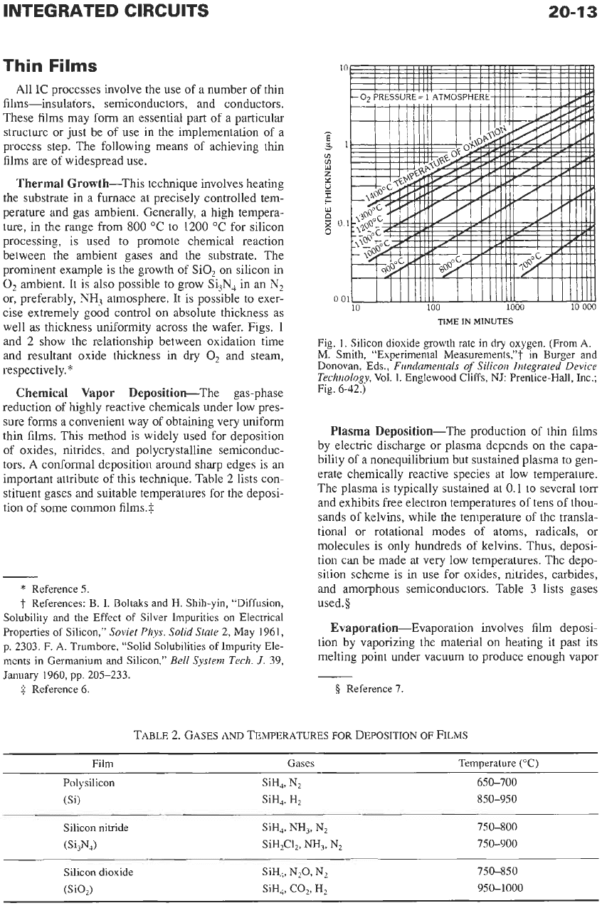
Thermal Growth-This technique involves heating
the substrate
in
a furnace at precisely controlled tem-
perature and gas ambient. Generally, a high tempera-
ture, in the range from
800
“C
to
1200
“C
for silicon
processing, is used to promote chemical reaction
between the ambient gases and the substrate. The
prominent example is the growth of SiO,
on
silicon in
0,
ambient. It is also possible to grow Si,N, in an
N,
or, preferably,
NH,
atmosphere. It
is
possible to exer-
cise extremely good control
on
absolute thickness as
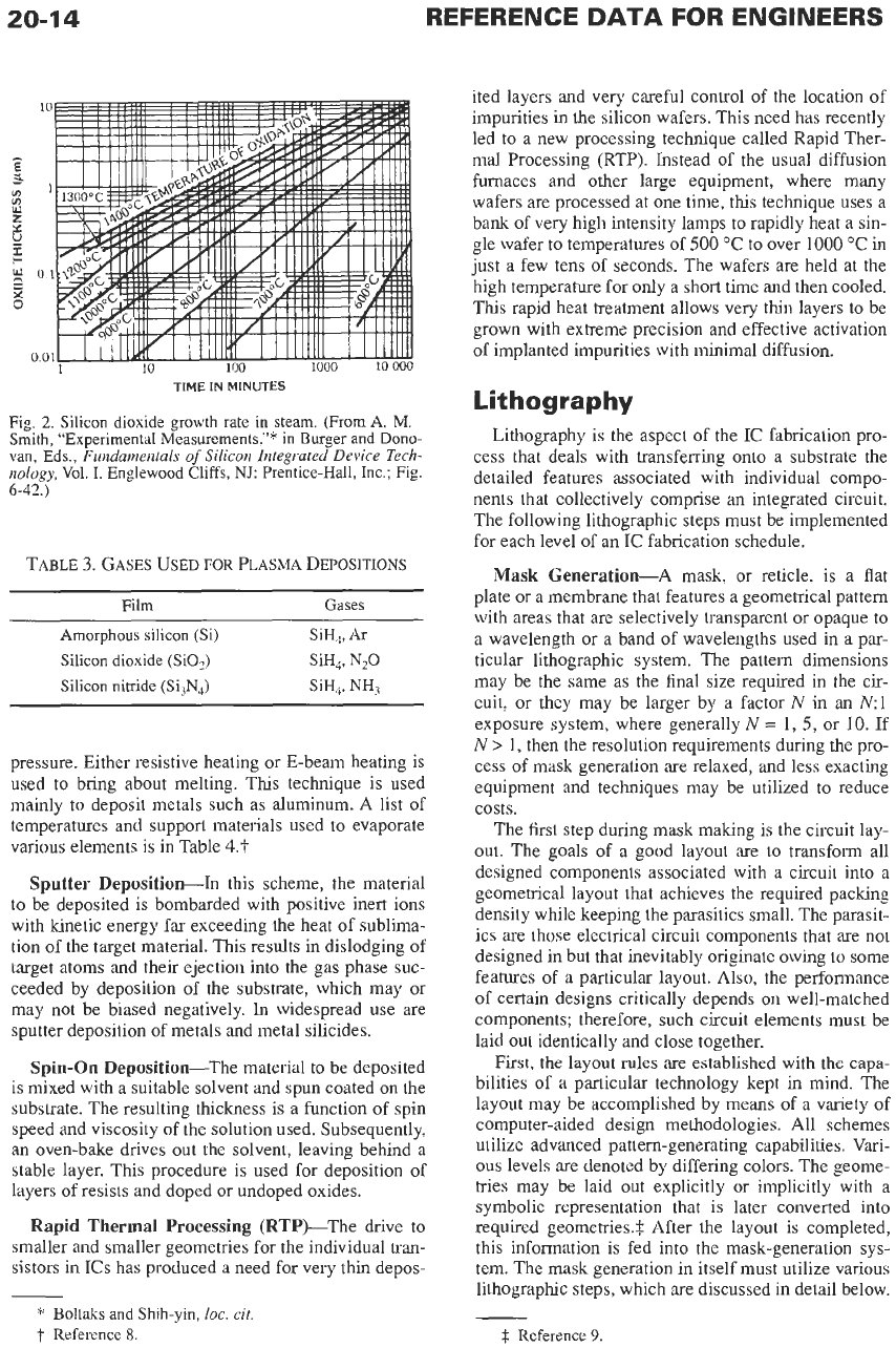
well as thickness uniformity across the wafer. Figs.
1
and
2
show the relationship between oxidation time
and resultant oxide thickness in dry
0,
and steam,
respectively.
*
Chemical Vapor Deposition-The gas-phase
reduction of highly reactive chemicals under low pres-
sure forms a convenient way
of
obtaining very uniform
thin films. This method is widely used for deposition
of oxides, nitrides, and polycrystalline semiconduc-
tors. A conformal deposition around sharp edges is an
important attribute of this technique. Table
2
lists con-
stituent gases and suitable temperatures for the deposi-
tion of some common films.$
*
Reference
5.
t
References: B. I. Boltaks and H. Shih-yin, “Diffusion,
Solubility and the Effect
of
Silver Impurities
on
Electrical
Properties of Silicon,”
Soviet Phys. Solid State
2, May 1961,
p. 2303.
F.
A.
Trumbore, “Solid Solubilities
of
Impurity Ele-
ments in Germanium and Silicon,”
Bell
System Tech.
J.
39,
J~~UXY
1960, pp. 205-233.
4
Reference 6.
TIME IN MINUTES
Fig.
1.
Silicon dioxide growth rate in dry oxygen. (From
A.
M.
Smith, “Experimental Measurements,”t in Burger and
Donovan, Eds.,
Fundamentals
of
Silicon Integrated Device
Technology,
Vol.
I.
Englewood Cliffs,
NJ:
Prentice-Hall, Inc.;
Fig. 6-42.)
Plasma Deposition-The production of thin
films
by electric discharge or plasma depends
on
the capa-
bility of a nonequilibrium but sustained plasma to gen-
erate chemically reactive species at low temperature.
The plasma is typically sustained at
0.1
to several torr
and exhibits free electron temperatures of tens of thou-
sands of kelvins, while the temperature of the transla-
tional or rotational modes of atoms, radicals, or
molecules is only hundreds of kelvins. Thus, deposi-
tion can be made at very low temperatures. The depo-
sition scheme is in use for oxides, nitrides, carbides,
and amorphous semiconductors. Table
3
lists gases
used.§
Evaporation-Evaporation involves film deposi-
tion by vaporizing the material
on
heating it past its
melting point under vacuum
to
produce enough vapor
5
Reference 7.
TABLE
2.
GASES
AND
TEMPERATURES
FOR
DEPOSITION
OF
FILMS
Film
Gases
Temperature
(“C)
Polysilicon SiH,,
N,
650-700
(Si) SiH,, H, 850-950
Silicon nitride SiH,,
NH,,
N, 750-800
(Si,N4)
SiH,Cl,,
NH,,
N, 750-900
Silicon dioxide
SiH,, N,O,
N,
750-850
(SiO,)
SiH,,
CO,,
H, 950-1000
20-1
4
REFERENCE
DATA
FOR ENGINEERS
TIME IN MINUTES
Fig.
2.
Silicon
dioxide
growth rate
in
steam. (From
A.
M.
Smith, "Experimental Measurements.""
in
Burger
and
Dono-
van, Eds.,
Fundamentals
of
Silicon Integrated Device Tech-
nology,
Vol.
I.
Englewood Cliffs, NJ Prentice-Hall, Inc.; Fig.
6-42.)
TABLE
3.
GASES USED
FOR
PLASMA
DEPOSITIONS
Film
Gases
~
Amorphous silicon (Si) SiH,,
Ar
Silicon dioxide (SiO,) SiH,,
N,O
Silicon
nitride
(Si,N,)
SiH,, NH,
pressure. Either resistive heating or E-beam heating is
used to bring about melting. This technique is used
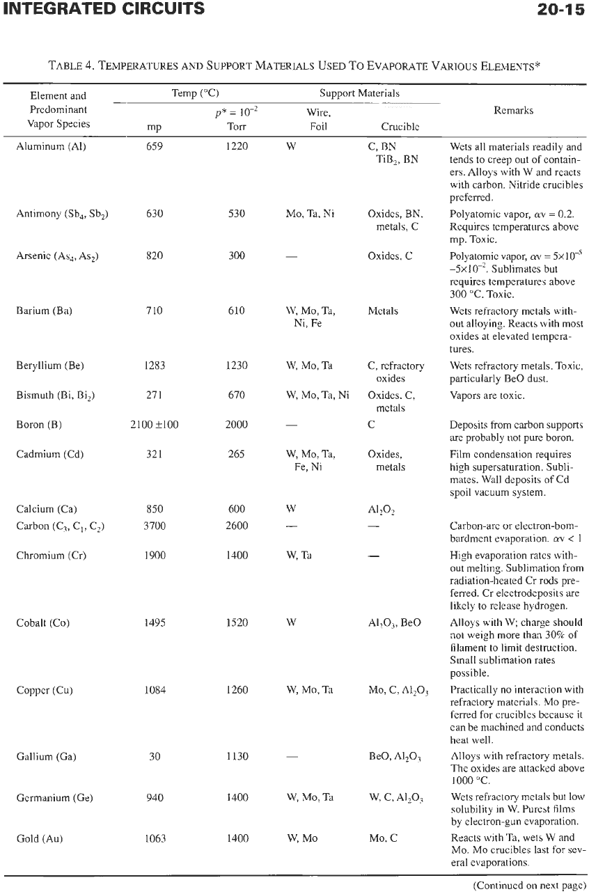
mainly to deposit metals such as aluminum. A list of
temperatures and support materials used to evaporate
various elements is in Table
4.t
Sputter Deposition-In this scheme, the material
to be deposited is bombarded with positive inert ions
with kinetic energy far exceeding the heat of sublima-
tion of the target material. This results in dislodging of
target atoms and their ejection into the gas phase suc-
ceeded by deposition of the substrate, which may or
may not be biased negatively.
In
widespread use are
sputter deposition of metals and metal silicides.
Spin-On Deposition-The material to be deposited
is mixed with a suitable solvent and spun coated on the
substrate. The resulting thickness is a function of spin
speed and viscosity of the solution used. Subsequently,
an oven-bake drives
out
the solvent, leaving behind a
stable layer. This procedure is used for deposition of
layers of resists and doped or undoped oxides.
Rapid Thermal Processing (RTP)-The drive to
smaller and smaller geometries for the individual tran-
sistors in
ICs
has produced a need for very thin depos-
*
Boltaks and Shih-yin,
loc. cit.
t
Reference
8.
ited layers and very careful control
of
the location of
impurities
in
the silicon wafers. This need has recently
led to a new processing technique called Rapid Ther-
mal Processing
(RTP).
Instead of the usual diffusion
furnaces and other large equipment, where many
wafers are processed at one time, this technique uses a
bank of very high intensity lamps to rapidly heat a sin-
gle wafer to temperatures of
500
"C
to over
1000
"C
in
just
a
few tens of seconds. The wafers
are
held
at
the
high temperature for only a short time and then cooled.
This rapid heat treatment allows very thin layers to be
grown with extreme precision and effective activation
of implanted impurities with minimal diffusion.
Lithography
Lithography is the aspect of the
IC
fabrication pro-
cess that deals with transferring onto a substrate the
detailed features associated with individual compo-
nents that collectively comprise an integrated circuit.
The following lithographic steps must be implemented
for each level of an
IC
fabrication schedule.
Mask Generation-A mask, or reticle, is a flat
plate or a membrane that features a geometrical pattern
with areas that
are
selectively transparent or opaque to
a wavelength or a band of wavelengths used in a par-
ticular lithographic system. The pattern dimensions
may be the same as the final size required in the cir-
cuit, or they may be larger by a factor
N
in an
N:l
exposure system, where generally
N
=
1,
5,
or
10.
If
N
>
1,
then the resolution requirements during the pro-
cess of mask generation are relaxed, and less exacting
equipment and techniques may be utilized to reduce
costs.
The first step during mask making is the circuit lay-
out. The goals of a good layout are
to
transform all
designed components associated with a circuit into a
geometrical layout that achieves the required packing
density while keeping the parasitics small. The parasit-
ics are those electrical circuit components that are not
designed in but that inevitably originate owing to some
features
of
a particular layout. Also, the performance
of
certain designs critically depends on well-matched
components; therefore, such circuit elements must be
laid out identically and close together.
First, the layout rules are established with the capa-
bilities of a particular technology kept
in
mind. The
layout may be accomplished by means of a variety of
computer-aided design methodologies. All schemes
utilize advanced pattern-generating capabilities. Vari-
ous
levels
are
denoted by differing colors. The geome-
tries may be laid out explicitly or implicitly with a
symbolic representation that is later converted into
required geometries.$ After the layout is completed,
this information is fed into the mask-generation sys-
tem. The mask generation in itself must utilize
various
lithographic steps, which are discussed in detail below.
j:
Reference
9.
20-1
5
TABLE
4.
TEMPERATURES AhD SUPPORT
MATERIALS
USED
TO
EVAPORATE
VARIOUS
ELEMEYTS"
Elementand
-
Temp ("C)
Support Materials
Predominant
p*
=
10-2 Wire, Remarks
Vapor Species mP
Torr
Foil Crucible
Aluminum (AI)
659 1220
Antimony (Sb,, Sb,)
630
Arsenic (As,, As,)
820
Barium (Ba)
Beryllium
(Be)
Bismuth (Bi, Bi,)
Boron
(B)
Cadmium (Cd)
530
300
710 610
1283 1230
21 1 670
2100 i.100 2000
321 265
Calcium (Ca)
850
Carbon (C3, C,, '2,)
3700
Chromium (Cr)
1900
Cobalt (Co)
1495
600
2600
1400
W
Mo,
Ta, Ni
W, Mo, Ta,
Ni,
Fe
W,
Mo,
Ta
W,
Mo,
Ta, Ni
-
W,
Mo,
Ta,
Fe. Ni
W
-
W, Ta
1520
W
Copper (Cu)
1084 1260
Gallium (Ga)
30 1130
Germanium
(Ge)
940
1400
Gold (Au)
1063 1400
W,
Mo,
Ta
W,
Mo, Ta
W,
Mo
C, BN
TiB,, BN
Oxides,
BN,
metals, C
Oxides, C
Metals
C, refractory
oxides
Oxides, C,
metals
C
Oxides,
metals
A1202
-
-
Al,O,, Be0
Mo,
C,
A120,
BeO, Al,O,
W, C, A1203
Mo, C
Wets all materials readily and
tends to creep out of contain-
ers. Alloys with W
and
reacts
with carbon. Nitride crucibles
preferred.
Polyatomic vapor,
av
=
0.2.
Requires temperatures above
mp. Toxic.
Polyatomic vapor,
M'
=
5x10''
-5~10-~.
Sublimates but
requires temperatures above
300
"C. Toxic.
Wets refractory metals with-
out alloying. Reacts with most
oxides at elevated tempera-
tures.
Wets refractory metals. Toxic,
particularly Be0 dust.
Vapors are toxic.
Deposits from carbon supports
are probably not
pure
boron.
Film condensation requires
high supersaturation. Subli-
mates. Wall deposits
of
Cd
spoil vacuum system.
Carbon-arc or electron-bom-
bardment evaporation.
av
<
1
High evaporation rates with-
out melting. Sublimation
from
radiation-heated Cr rods pre-
ferred. Cr electrodeposits are
likely to release hydrogen.
Alloys with
W
charge should
not weigh more than
30%
of
filament to limit destruction.
Small sublimation rates
possible.
Practically no interaction with
refractory materials.
Mo
pre-
ferred for crucibles because it
can be machined and conducts
heat well.
Alloys with refractory metals.
The oxides are attacked above
1000
"C.
Wets refractory metals but low
solubility in W. Purest films
by electron-gun evaporation.
Reacts with Ta, wets W and
Mo.
Mo crucibles last for
sev-
eral evaporations.
(Continued
on
next page)
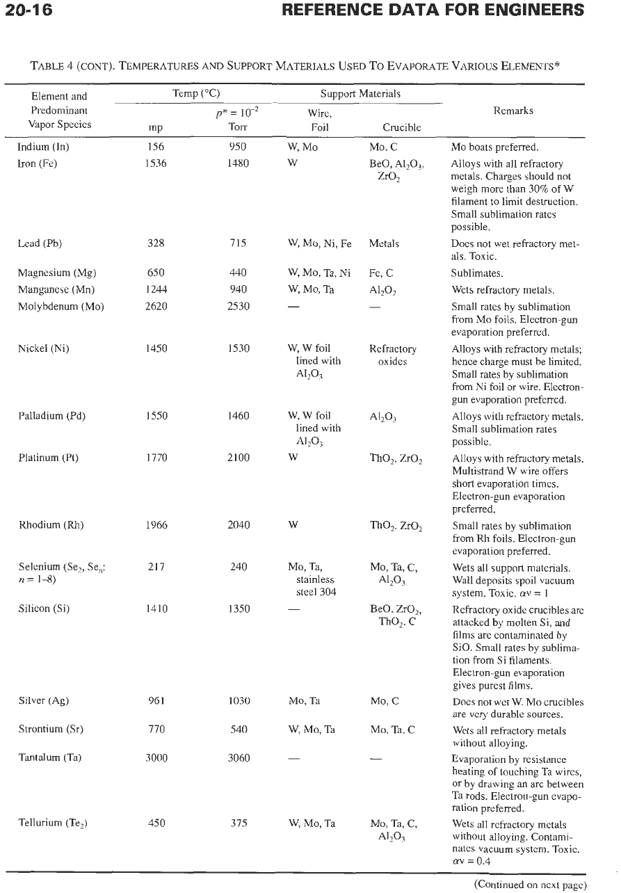
TABLE
4
(CONT). TEMPERATURES
AND
SUPPORT
MATERIALS
USED
TO
EVAPORATE
VARlOUS
ELEMENTS”
Element and Temp (“C)
Support Materials
Predominant
p“
=
10” Wire, Remarks
Vapor Species mP Torr Foil Crucible
Indium (In) 156 950
Iron (Fe) 1536 1480
W, Mo
W
Mo,
C
BeO,
A1,03,
ZrO,
Metals
Fe,
C
A1202
-
Refractory
oxides
A1203
Tho,, ZrO,
Tho,, ZrO,
Mo, Ta, C,
*lZ03
BeO,
ZrO,,
Tho,, C
Mo,
C
Mo, Ta, C
-
Mo,
Ta,
C,
A1203
Mo boats preferred.
Alloys with all refractory
metals. Charges should not
weigh more than 30% of W
filament to limit destruction.
Small sublimation rates
possible.
Does
not wet refractory met-
als. Toxic.
Sublimates.
Wets refractory metals.
Small rates by sublimation
from
Mo
foils. Electron-gun
evaporation preferred.
Alloys with refractory metals;
hence charge must be limited.
Small rates by sublimation
from Ni foil or wire. Electron-
gun evaporation preferred.
Alloys with refractory metals.
Small sublimation rates
possible.
Alloys with refractory metals.
Multistrand W wire offers
short evaporation times.
Electron-gun evaporation
preferred.
Small rates by sublimation
from Rh foils. Electron-gun
evaporation preferred.
Wets all support materials.
Wall deposits spoil vacuum
system. Toxic. av
=
1
Refractory oxide crucibles
are
attacked by molten Si, and
films are contaminated by
SiO. Small rates by sublima-
tion from Si filaments.
Electron-gun evaporation
gives purest films.
Does
not wet
W.
Mo
crucibles
are very durable sources.
Wets all refractory metals
without alloying.
Evaporation by resistance
heating of touching Ta wires,
or by drawing an arc between
Ta rods. Electron-gun evapo-
ration preferred.
Wets all refractory metals
without alloying. Contam-
nates vacuum system. Toxic.
(yv
=
0.4
Lead (Pb) 328 715
440
940
2530
W, Mo, Ni, Fe
Magnesium (Mg)
Manganese (Mn)
Molybdenum (Mo)
650
1244
2620
W, Mo, Ta, Ni
W, Mo, Ta
W, W foil
lined with
A1203
Nickel (Ni)
1450
1530
Palladium
(Pd)
Platinum (Pt)
1550
1770
1460
2100
W, W foil
lined with
A1203
W
Rhodium
(Rh)
1966
217
1410
2040 W
Selenium (Se,,
Sen:
n
=
1-8)
Silicon (Si)
240
1350
Mo, Ta,
stainless
steel 304
Silver (Ag)
Strontium (Sr)
Tantalum (Ta)
961
770
3000
1030
540
3060
Mo,
Ta
W,
Mo,
Ta
W,
Mo,
Ta
Tellurium
(Te,)
450 375
(Continued on next page)
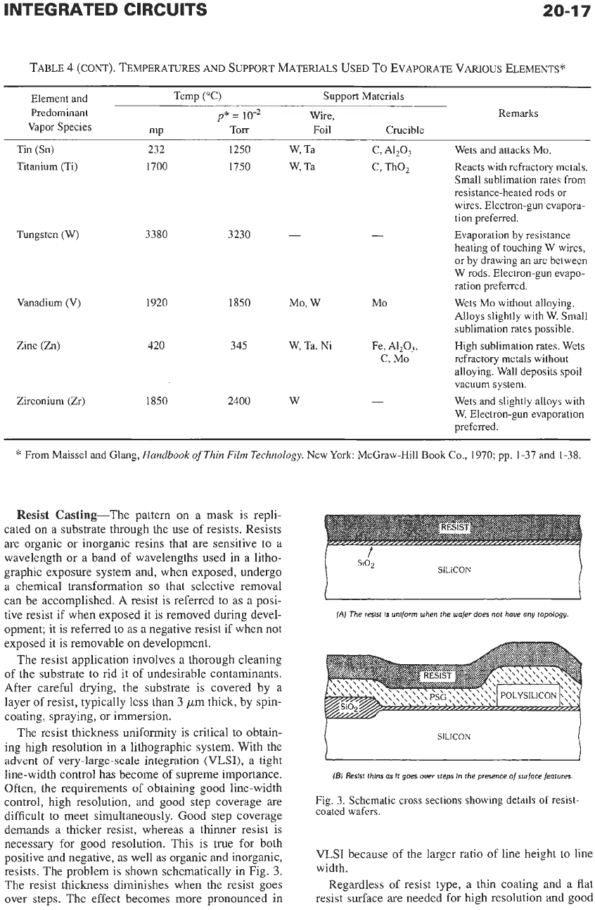
INTEGRATED CIRCUITS
20-1
7
TABLE
4
(CONT).
TEMPERATURES AND SUPPORT
MATERIALS
USED
TO
EVAPORATE
VARIOUS ELEMENTS*
Element and Temp ("C) Support Materials
Predominant
p*
=
10-2 Wire, Remarks
Vapor Species mp Torr Foil Crucible
Tin (Sn) 232 1250 W, Ta C, A1203 Wets and attacks
Mo
Titanium (Ti)
Tungsten
(W)
3380
3230
-
1700 1750 W, Ta C, Tho, Reacts with refractory metals.
Small sublimation rates from
resistance-heated rods or
wires. Electron-gun evapora-
tion preferred.
Evaporation by resistance
heating of touching W wires,
or
by drawing an arc between
W rods. Electron-gun evapo-
ration preferred.
Vanadium
(V)
1920 1850 Mo, W Mo Wets
Mo
without alloying.
Alloys slightly with W. Small
sublimation rates possible.
Zinc (Zn)
420
345 W, Ta, Ni Fe, A120,, High sublimation rates. Wets
alloying. Wall deposits spoil
vacuum system.
Zirconium (Zr)
1850
2400 W
-
Wets and slightly alloys with
W. Electron-gun evaporation
preferred.
C,
Ma
refractory metals without
*
From Maissel and Glang,
Handbook
of
Thin Film Technology.
New York McGraw-Hill
Book
Co., 1970; pp. 1-37 and 1-38.
Resist
Casting-The pattern on a mask is repli-
cated on a substrate through the use of resists. Resists
are organic or inorganic resins that are sensitive to a
wavelength or a band of wavelengths used in
a
litho-
graphic exposure system and, when exposed, undergo
a chemical transformation
so
that selective removal
can be accomplished. A resist is referred to
as
a posi-
tive resist if when exposed it is removed during devel-
opment; it is referred to as a negative resist if when not
exposed it is removable on development.
The resist application involves a thorough cleaning
of
the substrate to rid it
of
undesirable contaminants.
After careful drying, the substrate is covered by
a
layer of resist, typically less than
3
pm thick, by spin-
coating, spraying, or immersion.
The resist thickness uniformity is critical
to
obtain-
ing high resolution
in
a lithographic system. With the
advent
of
very-large-scale integration
(VLSI),
a tight
line-width control has become of supreme importance.
Often, the requirements of obtaining good line-width
control, high resolution, and good step coverage are
difficult to meet simultaneously. Good step coverage
demands a thicker resist, whereas a thinner resist is
necessary for good resolution. This is true for both
positive and negative, as well as organic and inorganic,
resists. The problem is shown schematically in Fig.
3.
The resist thickness diminishes when the resist goes
over steps. The effect becomes more pronounced in
SILICON
(A)
The resist
Is
unlforrn when the wafer does not have any topology.
SILICON
(BJ
Reslst thlns as
It
goes
over
steps
In
the presence
of
surface features.
Fig. 3. Schematic cross sections showing details
of
resist-
coated wafers.
VLSI
because of the larger ratio
of
line height to line
width.
Regardless of resist type, a thin coating and a flat
resist surface
are
needed
for
high resolution and good
20-1
8
REFERENCE
DATA
FOR ENGINEERS
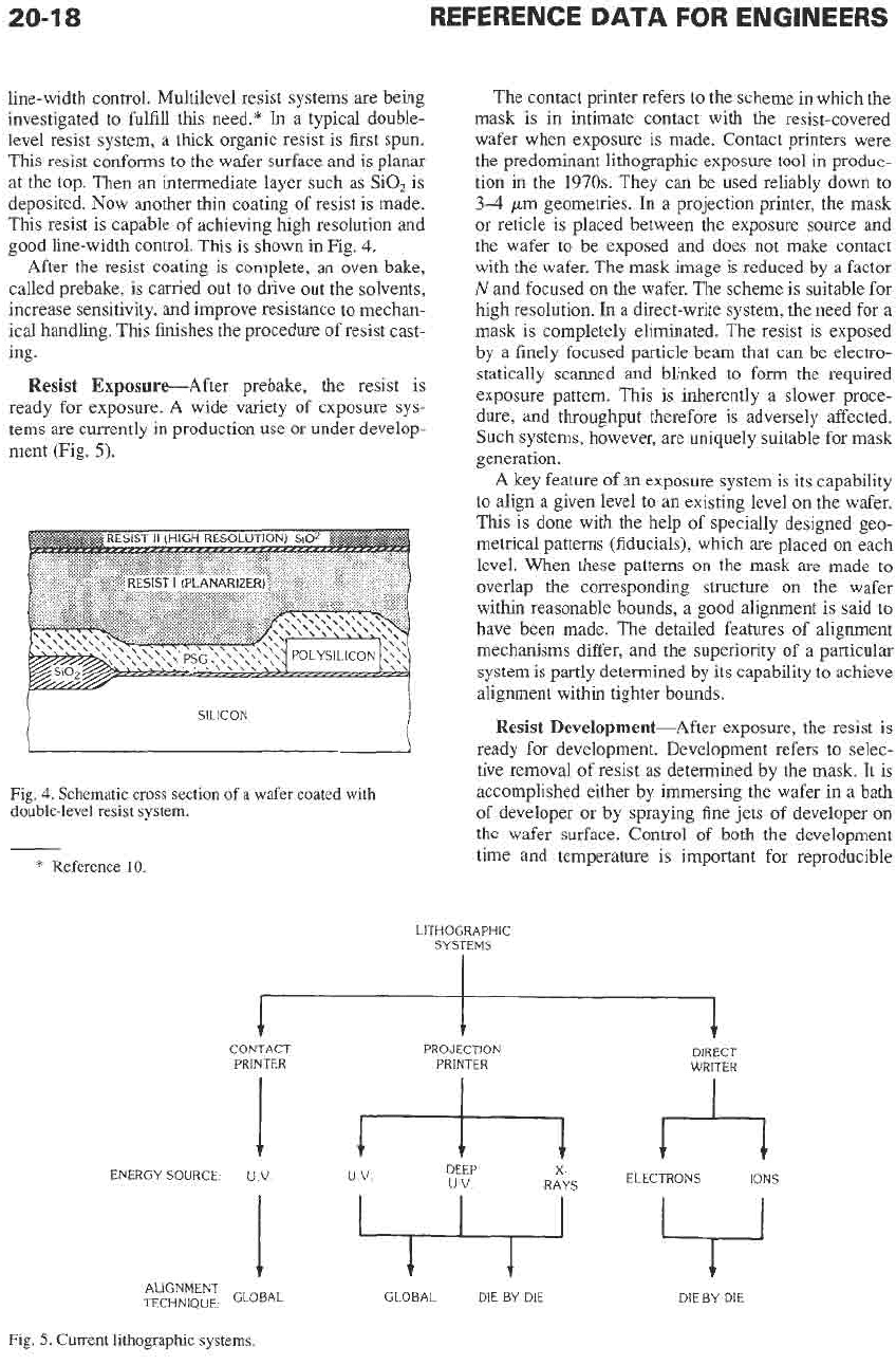
line-width control. Multilevel resist systems
are
being
investigated to fulfill this need.*
In
a typical double-
level resist system, a thick organic resist is first spun.
This resist conforms to the wafer surface and is planar
at the
top.
Then an intermediate layer such as SiO, is
deposited. Now another thin coating of resist is made.
This resist is capable of achieving high resolution and
good line-width control. This is shown in Fig.
4.
After the resist coating
is
complete, an oven bake,
called prebake, is carried out to drive out the solvents,
increase sensitivity, and improve resistance to mechan-
ical handling. This finishes the procedure
of
resist cast-
ing.
Resist Exposure-After prebake, the resist is
ready for exposure. A wide variety of exposure sys-
tems are currently in production use or under develop-
ment (Fig.
5).
SILICON
Fig.
4.
Schematic cross section of a wafer coated with
double-level
resist system.
*
Reference
10
The contact printer refers
to
the scheme in which the
mask is in intimate contact with the resist-covered
wafer when exposure is made. Contact printers were
the predominant lithographic exposure tool in produc-
tion in the
1970s.
They can be used reliably down to
3-4 pm geometries. In a projection printer, the mask
or
reticle is placed between the exposure source and
the wafer
to
be exposed and does not make contact
with the wafer. The mask image is reduced by a factor
N
and focused on the wafer. The scheme is suitable for
high resolution.
In
a direct-write system, the need for a
mask is completely eliminated. The resist is exposed
by a finely focused particle beam that can be electro-
statically scanned and blinked to form the required
exposure pattern. This is inherently a slower proce-
dure, and throughput therefore is adversely affected.
Such systems, however,
are
uniquely suitable for mask
generation.
A
key feature of an exposure system is its capability
to
align a given level to an existing level on the wafer.
This is done with the help of specially designed geo-
metrical patterns (fiducials), which are placed on each
level. When these patterns on the mask are made to
overlap the corresponding structure on the wafer
within reasonable bounds, a good alignment is said
to
have been made. The detailed features of alignment
mechanisms differ, and the superiority of a particular
system is partly determined by its capability
to
achieve
alignment within tighter bounds.
Resist Development-After exposure, the resist is
ready for development. Development refers
to
selec-
tive removal of resist as determined by the mask. It is
accomplished either by immersing the wafer in a bath
of
developer or by spraying fine jets of developer on
the wafer surface. Control of both the development
time and temperature is important for reproducible
LITHOGRAPHIC
SYSTEMS
CONTACT PROJECTION DIRECT
PRINTER PRINTER WRITER
IONS
x-
RAYS
ELECTRONS
DEEP
uv
ENERGY SOURCE
U
V
uv
ALIGNMENT
TECHNIQUE.
GLOBAL
DIE BY DIE
DIE BY DIE
Fig.
5.
Current lithographic systems.
INTEGRATED
CIRCUITS
20-1
9
line-width control. Fig.
6
shows schematically a posi-
tive-resist film after exposure and development. After
development,
the
wafer is rinsed to remove all
unwanted resist residues. Then the wafer is oven baked
to make the resist more resistant to subsequent chemi-
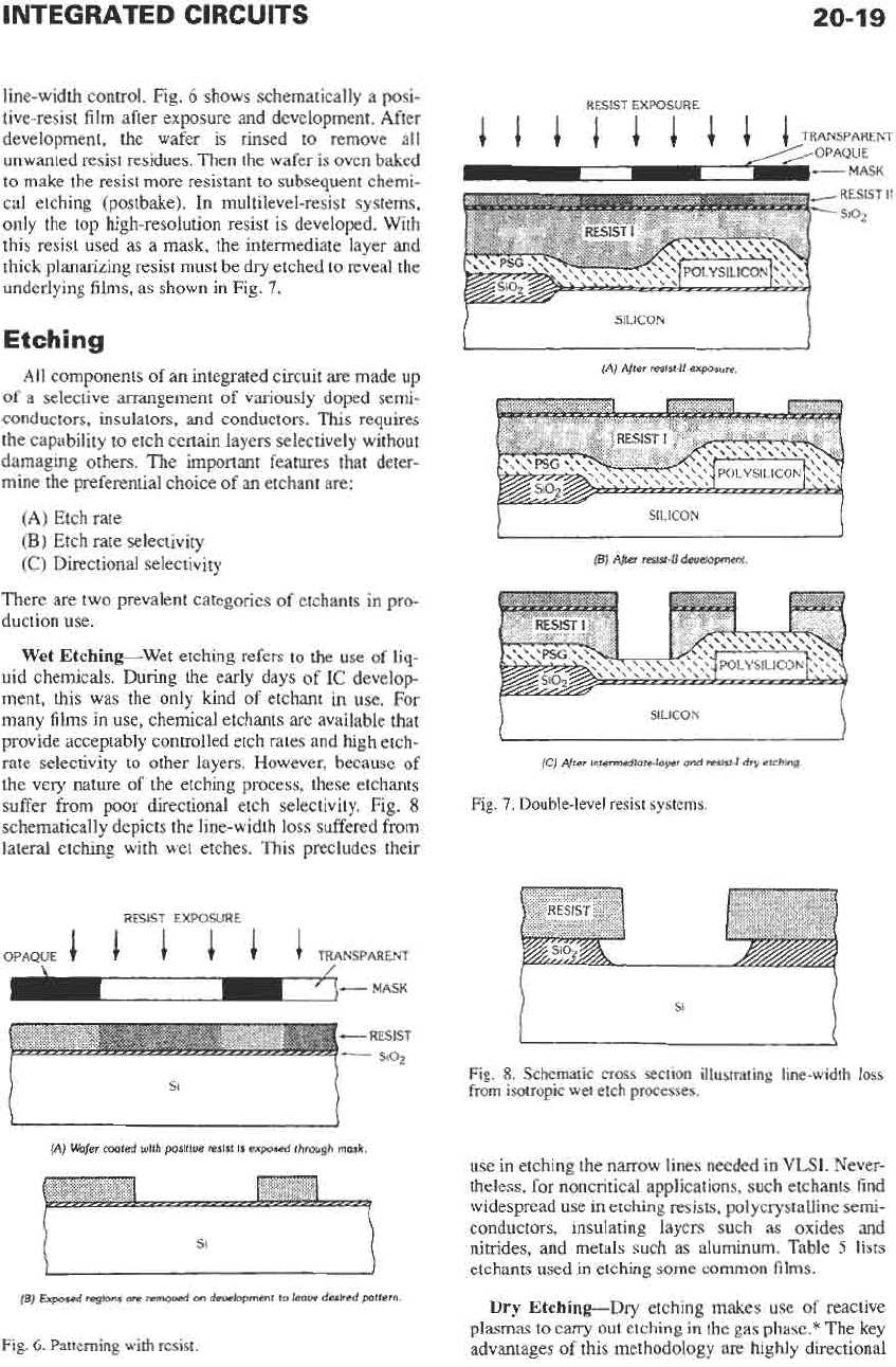
cal etching (postbake). In multilevel-resist systems,
only the top high-resolution resist is developed. With
this resist used as a mask, the intermediate layer and
thick planarizing resist must be
dry
etched to reveal the
underlying films, as shown in Fig.
7.
Etching
All components of an integrated circuit are made up
of a selective arrangement of variously doped semi-
conductors, insulators, and conductors. This requires
the capability to etch certain layers selectively without
damaging others. The important features that deter-
mine the preferential choice of
an
etchant
are:
(A) Etch rate
(B)
Etch rate selectivity
(C) Directional selectivity
There
are
two prevalent categories of etchants in pro-
duction use.
Wet
Etching-Wet etching refers to the use of liq-
uid chemicals. During the early days of IC develop-
ment, this was the only kind of etchant in use. For
many films in use, chemical etchants
are
available that
provide acceptably controlled etch rates and high etch-
rate selectivity to other layers. However, because
of
the very nature
of
the etching process, these etchants
suffer from poor directional etch selectivity. Fig.
8
schematically depicts the line-width loss suffered from
lateral etching with wet etches. This precludes their
RESIST EXPOSURE
OPAQUE
1
1
1
1
1
1
TRANSPARENT
-
MASK
[A)
Wafer coated with positive resist is exposed through mask.
Si
I
~
[E)
Exposed regions are removed
on
deuelopment to leave desired pattern.
Fig.
6.
Patterning with resist.
RESIST EXPOSURE
HI
I-
MASK
RESIST
I1
s102
SILICON
[A) After reslst.11 exposure.
[B)
After resist-I1 development.
I
SILICON
[C)
After intermediate-layer and resist-I dry etching.
Fig.
7.
Double-level resist systems.
Fig,
8.
Schematic cross section illustrating line-width loss
from isotropic wet etch processes.
use in etching the
narrow
lines needed in VLSI. Never-
theless, for noncritical applications, such etchants find
widespread use
in
etching resists, polycrystalline semi-
conductors, insulating layers such as oxides and
nitrides, and metals such as aluminum. Table
5
lists
etchants used in etching some common films.
Dry
Etching-Dry etching makes use of reactive
plasmas to carry out etching
in
the gas phase.* The key
advantages of this methodology
are
highly directional