Middleton W.M. (ed.) Reference Data for Engineers: Radio, Electronics, Computer and Communications
Подождите немного. Документ загружается.

20-20
REFERENCE
DATA
FOR ENGINEERS
TABLE
5.
ETCHANTS
USED
WITH
COMMON
FILMS
Temp.
Film Etch Composition (“C)
Silicon Planar etch 2 ml
HF,
15 ml
HNO,,
5 ml CH,COOH 25
Polysilicon Iodine etch 25
Silicon dioxide Bell
2
etch 54 ml H,O, 36 ml NH,F, 10 ml HF 25
Silicon nitride Hot phosphoric etch H,PO, 165
Aluminum
25
Titanium
-
90 ml H,O, 10 ml
HF
25
Tantalum
-
20 ml
HNO,,
10
ml
HF,
10
ml H,O 25
Molybdenum Dalton etch 92 g K,[Fe(CN),], 20
g
KOH,
300
ml H,O 25
Resists JlOO
100
50 ml
HF,
100
ml HNO,, 110
ml
CH,COOH,
0.3
g
I,
Phosphoric etch 55 ml H,PO,, 11 ml CH,OOH, 4.5
ml
HNO,, 2 ml H,O
*
*
Unknown, manufactured by Indust-Ri-Chem Lab., Richardson, Tex.
etch anisotropy and the facility to penetrate small
resist openings; these make it suitable for etching the
small geometries encountered in
VLSI.
By suitably
adjusting the constituents and proportions of etchant
species,
a
good etch-rate selectivity to other layers is
achieved. Plasma etching of resists, SiO,, Si,N,, Al,
Poly-Si, and metal silicides is
in
extensive use in the
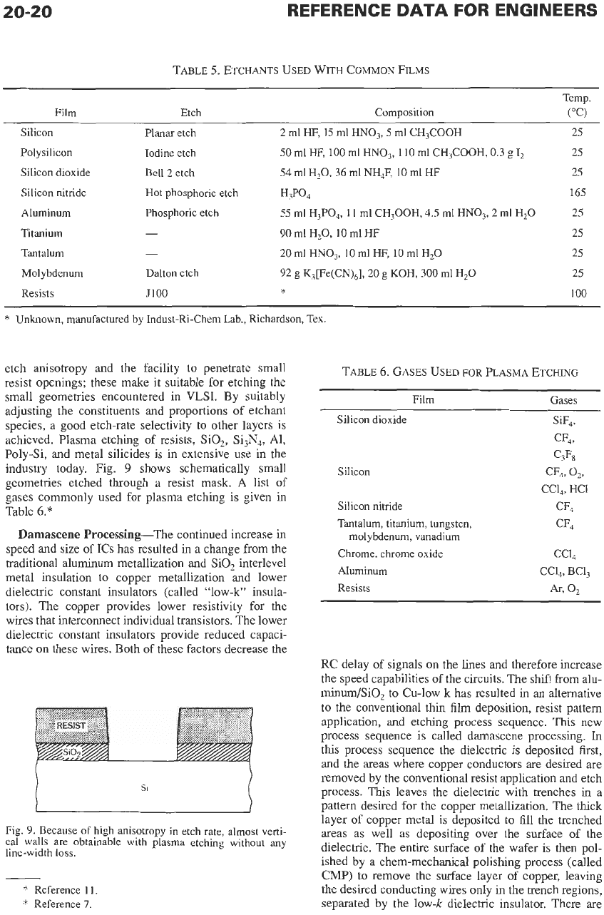
industry today. Fig.
9 shows schematically small
geometries etched through
a
resist mask.
A
list of
gases commonly used for plasma etching is given in
Table
6.”
Damascene Processing-The continued increase in
speed and size of ICs has resulted
in
a
change from the
traditional aluminum metallization and SiO, interlevel
metal insulation to copper metallization and lower
dielectric constant insulators (called “low-k” insula-
tors). The copper provides lower resistivity for
the
wires that interconnect individual transistors. The lower
dielectric constant insulators provide reduced capaci-
tance on these wires. Both
of
these factors decrease the
Fig.
9.
Because
of
high anisotropy in etch rate, almost vert-
cal walls are obtainable with plasma etching without any
line-width
loss.
*
Reference 11.
*
Reference
7.
TABLE
6.
GASES USED
FOR
PLASMA
ETCHING
Film Gases
Silicon dioxide
Silicon
Silicon nihide
Tantalum, titanium, tungsten,
molybdenum, vanadium
Chrome, chrome oxide
Aluminum
Resists
RC
delay of signals on the lines and therefore increase
the speed capabilities
of
the circuits. The shift from alu-
minutn/SiO, to Cu-low
k
has resulted in an alternative
to the conventional thin
film
deposition, resist pattern
application, and etching process sequence.
This
new
process sequence is called damascene processing.
In
this
process sequence the dielectric is deposited first,
and the areas where copper conductors are desired
are
removed by the conventional resist application and etch
process. This leaves the dielectric with trenches
in
a
pattern desired for the copper metallization. The thick
layer
of
copper metal is deposited to fill the trenched
areas
as
well
as
depositing over the surface
of
the
dielectric. The entire surface
of
the wafer is then pol-
ished by
a
chem-mechanical polishing process (called
CMP)
to remove the surface layer of copper, leaving
the desired conducting wires only
in
the trench regions,
separated by the low-k dielectric insulator. There are
INTEGRATED CIRCUITS
20-2
1
many details and variants of damascene processes that
may be found in the references.
Substrate
Doping
Procedures
All semiconductor devices rely
on
selective doping
of various areas, either n-type or p-type, to a required
concentration and depth. There are three predominant
techniques of introducing dopants in a controlled
manner.
Predeposition and Drive-In-The geometries to
be doped
are
lithographically defined
on
the substrate
in a mask layer such as oxide or nitride that is impervi-
ous
to the given dopant. Then
the
wafers are exposed
to the dopant source, which may be a gas, solid, or liq-
uid, in a well-controlled furnace at high temperature.
An
inert gas such as nitrogen or argon is used as a car-
rier for the dopant species.
The doping density in the substrate is a function of
predeposition temperature and time and is given by the
equation
where
N
is the doping density at a distancex below the sur-
tp
is
the predeposition time,
Dp
is the diffusion constant,
N,
is the surface concentration.
face,
The surface concentration is usually equal to the solid
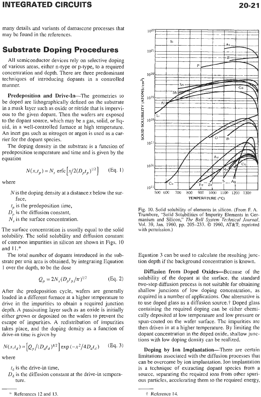
solubility. The solid solubility and diffusion constant
of common impurities in silicon are shown
in
Figs.
10
and
11.*
The total number
of
dopants introduced in the sub-
strate per unit area is obtained, by integrating Equation
1
over the depth, to be the dose
After the predeposition cycle, wafers are generally
loaded
in
a different furnace at a higher temperature to
drive in the impurities to obtain a required junction
depth.
A
passivating layer such as an oxide is initially
either grown or deposited
on
the wafers to prevent the
escape
of
impurities. A redistribution of impurities
takes place, and the doping density as a function of
drive-in time is given
by
where
t,
is the drive-in time,
D,
is the diffusion constant at the drive-in tempera-
ture.
Fig. 10. Solid solubility
of
elements in silicon. (From
E
A.
Trumbore, “Solid Solubilities
of
Impurity Elements in Ger-
manium
and
Silicon,”
The
Bell
System
Technical Journal,
Vol.
39, Jan. 1960,
pp.
205-233.
0
1960, AT&T reprinted
with permission.)
Equation
3
can be used to calculate the resulting junc-
tion depth if the background concentration is known.
Diffusion from Doped Oxides-Because of the
solubility of the dopant at the surface, the standard
two-step diffusion process is not suitable for obtaining
shallow junctions of low doping concentration, as
required in a number of applications. One alternative is
to use doped glass as a diffusion source.? Doped glass
containing the required doping can be either chemi-
cally deposited at low temperature and low pressure or
spun-coated
on
the wafer surface. The impurities are
then driven in at a higher temperature. By limiting the
dopant concentration
in
the doped oxide, shallow
junc-
tions with low doping density can be realized.
Doping by
Ion
Implantation-There are certain
limitations associated with the diffusion processes that
can be overcome by ion implantation.
Ion
implantation
is a technique
of
extracting dopant species from a
source, separating the required ions from other spuri-
ous
particles, accelerating them to the required energy,
i
Reference
14.
*
References 12 and
13.
20-22
0
01
REFERENCE
DATA
FOR ENGINEERS
Sb
I
I
TEMPERATURE
("C)
1300 1200 1100 1000
900
800
ior~~~~~1
I
I
8
I1
1
01
1000/T
(K)
(A)
Donor
Irnpurlfles.
TEMPERATURE
("C)
1300
1200
1100
1000
900
so0
1OI~'l'~~I'
I
I
I
'
I1
1
-
3
c
\
a
-
e
01
0
01
06
07
08
09
1000/T(K)
(B)
Acceptor lrnpurlfles
Fig.
11.
Diffusion constant
in
silicon.
(From A.
S.
Grove,
Physics
and
Technology
of
Semiconductor Devices,
New
York:
John Wiley
&
Sons, Inc.,
1967.)
and embedding them
in
the
substrate. The implantation
energy determines the impurity concentration.
To
a
good approximation, the implanted ions settle with a
gaussian distribution given by Reference 15:
where
N(x)
is the dopant concentration at a distancex
below the surface,
Q is the ion dose,
Rp
is the ion range,
ARp
is the range straggle.
The values for
Rp
and
Up
as a function of implant
energy are available in published tables. Table
7
gives
values for usual dopants in silicon.*
With this technique, it is possible
to
exercise a tight
control on both the depth and the concentration of
dopants, which is of prime importance in
VLSI.
By
choosing multiple implant energies and doses, a vari-
ety
of
intended profiles can be approximated. The ion
implantation is followed by a thermal anneal, which
activates the dopants and anneals
out
the crystal dam-
age produced by the process.
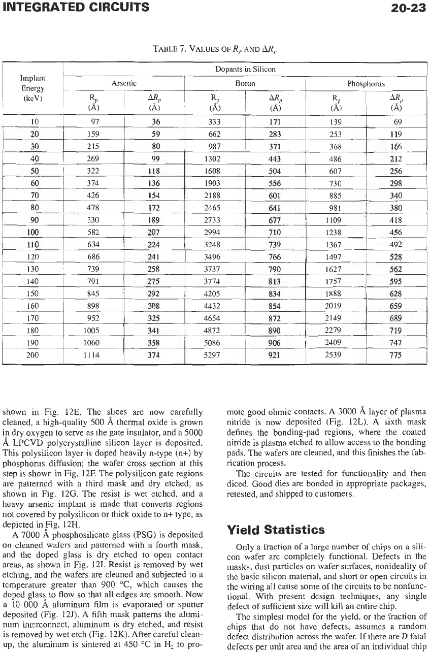
An
IC
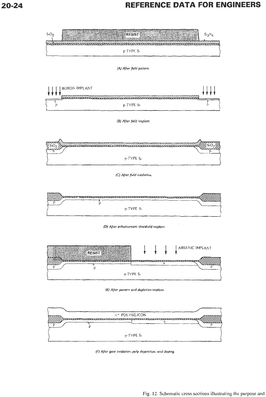
Process Example-
NMOS
Process
The information presented above can best be con-
solidated by illustrating an
IC
fabrication process. For
this purpose, we have chosen to discuss NMOS tech-
nology, whose typical basic process flow can be illus-
trated with the help of Fig.
12.
The starting material is p-type silicon
in
wafers that
are carefully cleaned and thermally oxidized
in
steam
to obtain an SiO, thickness of
300
A.
An
GPCVD
Si,N, is now deposited to a thickness of
2000
A.
Next,
the isolation regions are defined by using a moat mask
as shown
in
Fig.
12A.
Sequentially,
dry
plasma etching
of nitride and oxide is carried out, with resist protect-
ing the areas not to be etched. Resist is removed by
JlOO wet etch, and a low-energy boron implant is
made that raises the p-type doping density in the
opened windows but does not penetrate through the
nitride and oxide stack, as illustrated in Fig.
12B.
Slices are then cleaned and thermally oxidized
in
steam to oxidize the exposed regions to obtain an SiO,
thickness
of
7000
A;
nitride prohibits oxidation of
other areas, as shown in Fig.
12C.
Nitride is now wet
etched in hot phosphoric acid, and an unmasked boron
implant is made to adjust the threshold voltage of
enhancement-mode devices, as shown in Fig.
12D.
The depletion-mode-device region is defined by a
second mask in order to adjust the threshold voltage of
depletion-mode devices.
An
arsenic implant dopes the
exposed silicon areas n-type near the surface.
This
is
*
Reference
16.
INTEGRATED CIRCUITS
10
20
30
40
50
TABLE
7.
VALUES
OF
R,
AND
up
97 36 333 171 139 69
159 59 662
283 253 119
215 80 987 371 368 166
269 99 1302
443 486 212
322 118
1608
I
504
607 256
I
20-23
shown in Fig.
12E.
The slices
are
now carefully
cleaned, a high-quality
500
A
thermal oxide is grown
in
dry
oxygen to serve as the gate insulator, and a
5000
A
LPCVD polycrystalline silicon layer is deposited.
This polysilicon layer is doped heavily n-type
(n+) by
phosphorus diffusion; the wafer cross section at this
step is shown in Fig.
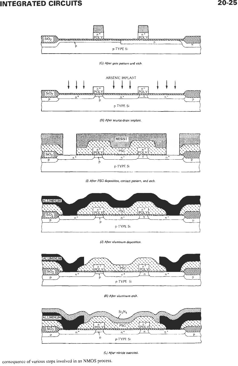
12F. The polysilicon gate regions
are patterned with a third mask and dry etched, as
shown
in
Fig. 12G. The resist is wet etched, and a
heavy arsenic implant is made that converts regions
not covered by polysilicon or thick oxide to n+ type, as
depicted
in
Fig. 12H.
A
7000
A phosphosilicate glass (PSG) is deposited
on cleaned wafers and patterned with a fourth mask,
and the doped glass is
dry
etched to open contact
areas, as shown in Fig.
121. Resist is removed by wet
etching, and the wafers are cleaned and subjected to a
temperature greater than
900
"C,
which causes the
doped glass to
flow
so
that all edges
are
smooth. Now
a
10
000
A
aluminum film is evaporated or sputter
deposited (Fig.
125). A fifth mask patterns the alumi-
num interconnect, aluminum is dry etched, and resist
is removed by wet etch (Fig.
12K). After careful clean-
up, the aluminum is sintered at
450
"C in
H2
to pro-
mote good ohmic contacts. A
3000
A
layer of plasma
nitride is now deposited (Fig.
12L). A sixth mask
defines the bonding-pad regions, where the coated
nitride is plasma etched to allow access to the bonding
pads. The wafers
are
cleaned, and this finishes the fab-
rication process.
The circuits
are
tested for functionality and then
diced. Good dies are bonded in appropriate packages,
retested, and shipped
to
customers.
Yield Statistics
Only
a fraction
of
a
large
number of chips on a
sili-
con wafer are completely functional. Defects in the
masks, dust particles on wafer surfaces, nonideality of
the basic silicon material, and short
or
open circuits in
the wiring
all
cause some of the circuits to be nonfunc-
tional. With present design techniques, any single
defect
of
sufficient size will kill
an
entire chip.
The simplest model for the yield, or the fraction of
chips that do not have defects, assumes a random
defect distribution across the wafer. If there
are
D
fatal
defects per unit area and the area
of
an
individual chip
20-24
REFERENCE
DATA
FOR ENGINEERS
p
TYPE
SI
(A) After peld pottern.
BORON
IMPLANT
p
TYPE
SI
(BJ
After field implant
(C)
After field oadatlon.
(D)
After enhancement threshold Implont.
p-TYPE
SI
(E)
After pattern
and
depletion implant
P
p-TYPE
Si
(FI
After gate oxldarlon, poly deposition, and doping
Fig.
12.
Schematic cross sections illustrating the purpose
and
INTEGRATED CIRCUITS
20-25
(G)
After gate pattern and etch
ARSENIC IMPLAET
p-TYPE
SI
(HI
After sourcedraln Implant.
(I)
After
PSG
deposition, contact pattern, and etch.
P
p.TYPE
SI
(JI
After alumlnum deposltlon
(K)
After aluminum etch.
(LJ
After nltrlde ouercoat.
consequence
of
various
steps
involved
in
an
NMOS
process.
20-26
REFERENCE
DATA
FOR ENGINEERS
is
A,
then the probability that a chip has
n
flaws is, in
the simplest case, given by the
Poisson
distribution
P,(DA).
The probability of a good chip is:
Po
(DA)
=
e-DA
(Eq.
5)
While this equation is not rigorously applicable to fab-
rication processes, it is a good approximate model for
estimating the yield of various design alternatives.
IC
DESIGN*
The design of integrated circuits requires the syn-
thesis and analysis of a large number of active ele-
ments. The classical form of analysis can be extended
to integrated circuits, whereas the focus of synthesis
goes beyond the classical notions inasmuch as the geo-
metric layout
of
the circuit topography for integrated
circuits
is
a major fraction of the circuit synthesis. The
electrical aspects of circuit design derive
from
the con-
siderations that are laid out in Chapter
18,
with certain
constraints based on the scale of integration. The
design of
the
circuit topography is unique to integrated
circuits and has evolved as a major discipline.
Modeling and Simulation
The design of integrated circuits requires the electri-
cal analysis of circuits that contain a large number of
elements. For
LSI
or VLSI circuits,
this
involves the
simulation of up to tens of millions
of
circuit elements
if the total circuit response is to be examined. The eval-
uation of
this
class of circuits is extremely computer-
intensive.
In
most cases, it is not practical to simulate
the circuit with classical time- or frequency-domain
analysis at the transistor level. The current practice for
simulation and analysis of such classes of circuits is to
adopt a hierarchical procedure with different levels of
abstraction at each level. The design
of
an
LSI
logic cir-
cuit would involve a typical modeling hierarchy such as
that in Chart
1.
The top of the hierarchy is an abstract definition of
the architecture of the circuit, which is used to provide
a guideline for the various ways of accomplishing the
objective of the circuit. It trades off, for example, the
use of pipeline processing versus serial processing.
The
behavioral level
of
simulation actually involves
CHART 1.
DESIGN
HIERARCHY
FOR
LSI CIRCUITS
Architecture
simulation
Behavioral simulation
Functional simulation
Logic simulation
Transistor simulation
the definition of the major blocks of the circuit and
their interaction, with the details of the overall data or
control flow to accomplish the objective of the chip
being examined. The functional level actually
describes the overall logical response of the major
blocks, relating
the
logical inputs and outputs with
no
details of internal realization of logic in the block. The
logic-simulation level details the realization of each
block at the gate level, provides logic minimization,
and in some cases introduces the notion of relative tim-
ing. The transistor-level simulation considers the tran-
sient response of the circuit, including the detailed
simulation of all elements of the circuit. The key to the
usefulness of this hierarchical simulation
is
the ability
to mix the different levels of abstraction to examine
the performance of the entire circuit with focus on one
block at a time. Such mixed-mode simulators are being
evolved, and common hardware-description languages
that operate on a unified data base that is accessed by
any level
of
the hierarchy are now available.
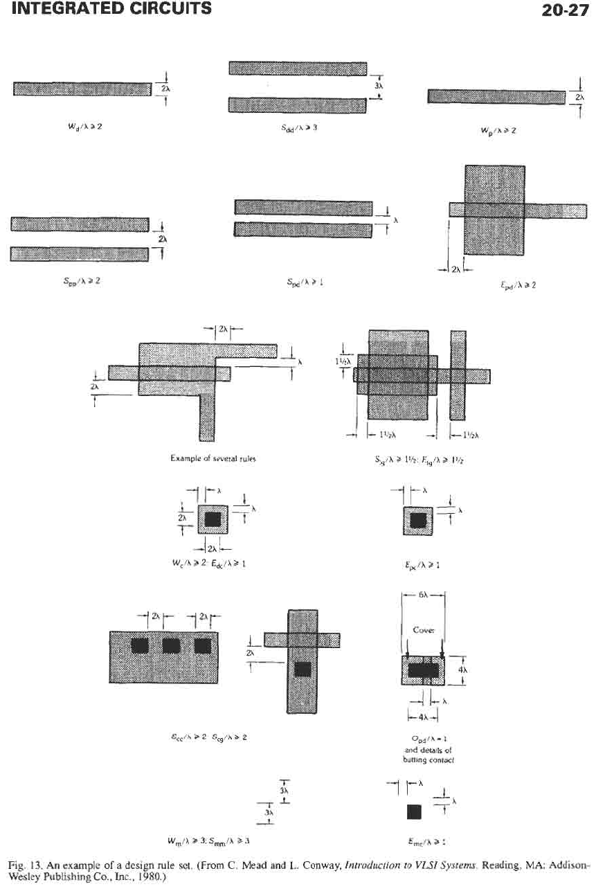
Topological Realization of
Circuits
The design of integrated circuits differs from the
design of board-level circuits in the importance of the
actual physical realization of the active elements and
interconnections. Typical LSI circuits have many thou-
sands of active elements and interconnections that
must be topologically related to each other. This
requires the interaction of the device physics, process
technology constraints, and topological constraints. To
obtain a practical solution to this complex interactive
design environment, it is generally accepted practice to
describe the process constraints
in
the form of a design
rule package. This design rule package is a simple
description of the lateral spatial relationship of the var-
ious active-element forming geometries as well as the
wiring.
A
simple example of design rules is shown in
Fig.
13.
The original concept
of
the design rules was
governed by the constraints of the technology only.
However, the design data base for the geometrical
description
of
the circuit for VLSI circuits is very
large, and some constraints that limit the size of this
data base have been introduced into the design rules.+
This is simply
a
quantization
of
the minimum spatial
distance describing any technology constraint. This
kind of quantization is equivalent to the definition of
the finest grid
on
which a geometry must fall.
There
are
two major approaches to the realization
of
the geometrical data base for an IC. The first is the
classical approach in which the complete drawing
of
each individual section is introduced into the data
base in detail. This is a tedious and inefficient way
of
generating data. The preferred approach
to
data entry
is through a symbolic description of the layout
in
which the definitions of the often-used elements are
*
Reference
9.
C
Reference
9.
INTEGRATED CIRCUITS
20-27
I
7
I
W,/X
2
2
Wp/h
b
2
Example
of
several rules
S,,/X
3
l’h.
E,@
b
l’h
S,,/X
2
2:
&,/A
>
2
Ep,/X
2
1
I-
a.
-I
O@/h
=
1
and
details
of
butting
contact
T
3X
m7
71
3X
1
W,/h
3
3:
S,,/X
2
3
E,,/x
2
I
Fig.
13.
An
example
of
a design
rule
set.
(From
C.
Mead and
L.
Conway,
Introduction
to
VLSI
Systems.
Reading,
MA:
Addison-
Wesley Publishing Co.,
Inc.,
1980.)
20-28
REFERENCE DATA FOR ENGINEERS
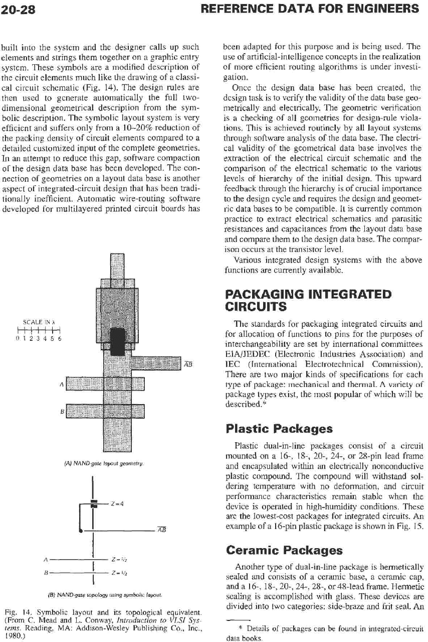
built into the system and the designer calls up such
elements and strings them together on a graphic entry
system. These symbols are a modified description of
the circuit elements much like the drawing of a classi-
cal circuit schematic (Fig.
14).
The design rules are
then used to generate automatically the full two-
dimensional geometrical description from the sym-
bolic description. The symbolic layout system is very
efficient and suffers only from a 1620% reduction of
the packing density of circuit elements compared to a
detailed customized input of the complete geometries.
In
an attempt to reduce
this
gap, software compaction
of the design data base has been developed. The con-
nection of geometries on a layout data base is another
aspect
of
integrated-circuit design that has been tradi-
tionally inefficient. Automatic wire-routing software
developed for multilayered printed circuit boards has
SCALE
IN
A
012345
ttt+tt
-1
6
A
B
(A)
NAND-gate layout geometry
A
z=1/2
6
'
z=
'/2
I
(Bj
NAND-gate topology using symbolic layout
Fig.
14.
Symbolic layout and its topological equivalent.
(From C.
Mead
and
L.
Conway,
Introduction
to
VLSI
Sys-
tems.
Reading, MA: Addison-Wesley Publishing Co., Inc.,
1980.)
been adapted for this purpose and is being used. The
use of artificial-intelligence concepts in the realization
of more efficient routing algorithms is under investi-
gation.
Once the design data base has been created, the
design task is to verify the validity of the data base geo-
metrically and electrically. The geometric verification
is a checking of all geometries for design-rule viola-
tions.
This
is achieved routinely by all layout systems
through software analysis
of
the data base. The electri-
cal validity
of
the geometrical data base involves the
extraction of the electrical circuit schematic and the
comparison
of
the electrical schematic to the various
levels of hierarchy of the initial design. This upward
feedback through
the
hierarchy is of crucial importance
to the design cycle and requires the design and geomet-
ric data bases to be compatible. It
is
currently common
practice to extract electrical schematics and parasitic
resistances and capacitances from the layout data base
and compare them to the design data base. The compar-
ison occurs at the transistor level.
Various
integrated design systems with the above
functions are currently available.
PACKAGING INTEGRATED
CIRCUITS
The standards for packaging integrated circuits and
for allocation of functions to pins for the purposes of
interchangeability are set by international committees
EIA/JEDEC (Electronic Jidustries Association) and
IEC
(International Electrotechnical Commission).
There are two major kinds of specifications for each
type of package: mechanical and thermal. A variety of
package types exist, the most popular of which will be
described.*
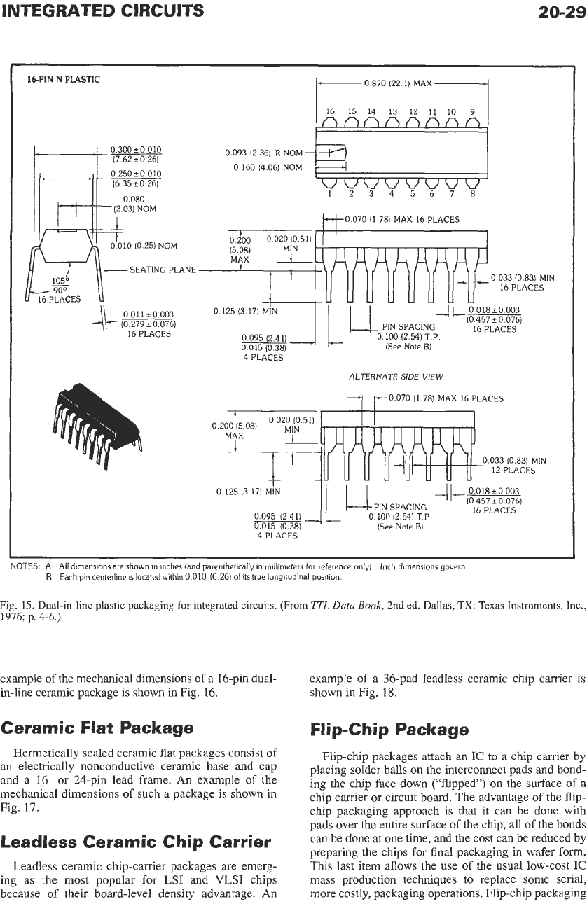
Plastic Packages
Plastic dual-in-line packages consist of a circuit
mounted on a 16-,
IS-,
20-, 24-, or 28-pin lead kame
and encapsulated within an electrically nonconductive
plastic compound. The compound will withstand sol-
dering temperature with
no
deformation, and circuit
performance characteristics remain stable when the
device is operated
in
high-humidity conditions. These
are
the lowest-cost packages for integrated circuits. An
example of a 16-pin plastic package is shown
in
Fig.
15.
Ceramic Packages
Another type
of
dual-in-line package is hermetically
sealed and consists of a ceramic base, a ceramic cap,
and a
16-,
18-,
20-,
24-,
28-, or 48-lead frame. Hermetic
sealing is accomplished with glass. These devices are
divided into
two
categories: side-braze and frit seal. An
*
Details of packages can be found in integrated-circuit
data books.
INTEGRATED
CIRCUITS
fq
0
093
12
361
R
NOM
0 160 (4 061 NOM
20-29
16-PIN N PLASTIC
0
300+0.010
(7.62fO 26)
0
25020 010
(6 35
’.
0 261
0
080
SEATING PLANE
0
011fO
003
(0
279
f
0 076)
16 PLACES
-
0.870
(22.1)
MAX
I
I
16 15 14
13
12 11
10
9
lAnnnnnnA
0
033
(0
83)
MIN
16 PLACES
!--
0
018fO
003
(0
457fO 076)
16 PLACES
0
125
(3
17)
MiN
0 095
(2
411
4 PLACES
6-iKZm
ALTERNATE
SIDE
VIEW
0.070 (1.78)
MAX
16 PLACES
0
033
(0
83)
MIN
4
PLACES
NOTES:
A
AI1
dimensions are shown
in
inches (and parenthetically in millimeters
for
reference only]
B
Each
pin
centerline
IS
located
within
0
010
(0.26)
of
its true longitudinal position.
Inch
dimensions
govern
Fig.
15.
Dual-in-line plastic packaging
for
integrated circuits.
(From
ZTL
Datu
Book,
2nd ed. Dallas,
TX:
Texas Instruments, Inc.,
1976;
p.
4-6.)
example
of
the mechanical dimensions
of
a 16-pin dual-
in-line ceramic package is shown
in
Fig. 16.
Ceramic Flat Package
Hermetically sealed ceramic flat packages consist
of
an electrically nonconductive ceramic base and cap
and a 16- or 24-pin lead frame.
An
example
of
the
mechanical dimensions of such a package is shown
in
Fig.
17.
Leadless Ceramic Chip Carrier
Leadless ceramic chip-canier packages are emerg-
ing as the most popular for
LSI
and VLSI chips
because
of
their board-level density advantage.
An
example of a 36-pad leadless ceramic chip carrier
is
shown in Fig.
18.
FI
i
p-
Ch
i
p
Package
Flip-chip packages attach an
IC
to a chip carrier
by
placing solder balls
on
the interconnect pads and bond-
ing the chip face down (“flipped”) on the surface
of
a
chip carrier or circuit board. The advantage of the flip-
chip packaging approach is that it can be done with
pads over the entire surface of
the
chip, all of the bonds
can be done at one time, and the cost can be reduced by
preparing the chips for final packaging in wafer
form.
This last item allows the use of the usual low-cost
IC
mass production techniques to replace some serial,
more costly, packaging operations. Flip-chip packaging