Middleton W.M. (ed.) Reference Data for Engineers: Radio, Electronics, Computer and Communications
Подождите немного. Документ загружается.

20-40
REFERENCE
DATA
FOR ENGINEERS
the ITRS projections for these memory features over
the next several years.
Externally, memory chips typically require the
application of a binary address input to locate the
information.
A
set of control or mode-setting signals is
needed to tell the memory to read or write, and the
memory circuit provides the desired information after
a time interval that is called the access time for the
memory. Memories are organized to provide either one
bit of data at a time or one byte of data at a time. The
choice of the data word is a system partitioning func-
tion.
In
addition, other system options such as power-
down modes are common. Many different memories
are available that fall into the categories described
here. The various manufacturers’ data books and
applications books should be consulted for detailed
information.
Read-only Memories (ROM)
Read-only memories have information programmed
into
them during manufacture. They act as tables of
data that can be accessed by the system at any time.
This class of memories is extremely useful in the stor-
age
of
programs, operating systems, fixed utilities for a
system, etc.
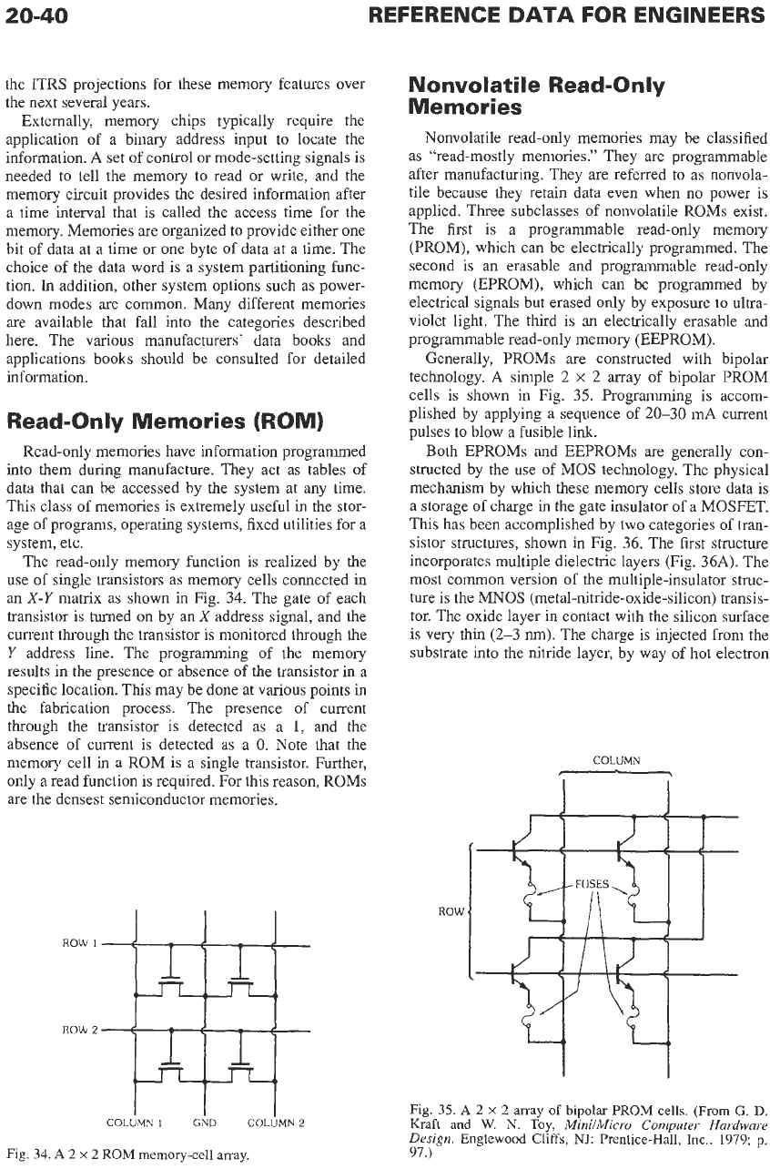
The read-only memory function is realized by the
use of single transistors as memory cells connected
in
an
X-Y
matrix as shown in Fig. 34. The gate of each
transistor is turned on by an
X
address signal, and the
current through the transistor is monitored through the
Y
address line. The programming of the memory
results in the presence or absence of the transistor in a
specific location. This may be done at various points in
the fabrication process. The presence of current
through the transistor is detected as a
1,
and the
absence of current is detected as a
0.
Note that the
memory cell
in
a ROM is a single transistor. Further,
only a read function is required. For this reason, ROMs
are the densest semiconductor memories.
ROW
ROW
1
ROW
2
Fig.
34.
A
2
x
2
ROM
memory-cell array.
Nonvolat
i
le Read-On ly
Memories
Nonvolatile read-only memories may be classified
as “read-mostly memories.” They are programmable
after manufacturing. They are referred to as nonvola-
tile because they retain data even when
no
power is
applied. Three subclasses of nonvolatile ROMs exist.
The first is
a
programmable read-only memory
(PROM), which can be electrically programmed. The
second is an erasable and programmable read-only
memory (EPROM), which can be programmed by
electrical signals but erased only by exposure to ultra-
violet light. The third is
an
electrically erasable and
programmable read-only memory (EEPROM).
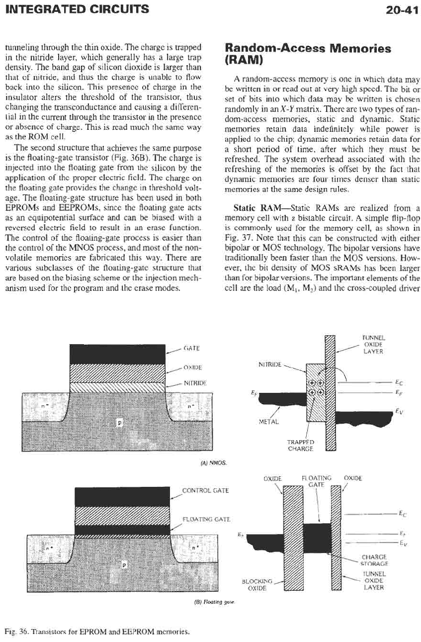
Generally, PROMS are constructed with bipolar
technology.
A
simple
2
x
2 array of bipolar
PROM
cells is shown in Fig. 35. Programming is accom-
plished by applying a sequence of 20-30
mA
current
pulses to blow
a
fusible link.
Both EPROMs and EEPROMs are generally con-
structed by the use of MOS technology. The physical
mechanism by which these memory cells store data is
a storage of charge in the gate insulator of a MOSFET.
This has been accomplished by two categories of tran-
sistor structures, shown in Fig. 36. The first structure
incorporates multiple dielectric layers (Fig. 36A). The
most common version of the multiple-insulator struc-
ture is the
MNOS
(metal-nitride-oxide-silicon) transis-
tor. The oxide layer in contact with the silicon surface
is very thin
(2-3
nm).
The charge
is
injected from the
substrate into the nitride layer, by way of hot electron
COLUMN
Fig.
35.
A
2
x
2
array of bipolar
PROM
cells. (From G.
D.
Kraft
and
W.
N.
Toy,
MinilMicro
Computer
Hardware
Design.
Englewood Cliffs,
NJ:
Prentice-Hall, Inc., 1979;
p.
97.)
INTEGRATED CIRCUITS
20-41
tunneling through the thin oxide. The charge is trapped
in the nitride layer, which generally has a large trap
density. The band gap of silicon dioxide is larger than
that of nitride, and thus the charge is unable to flow
back into the silicon. This presence of charge in the
insulator alters the threshold of the transistor, thus
changing the transconductance and causing a differen-
tial in the current through the transistor in the presence
or absence of charge. This
is
read much the same way
as the ROM cell.
The second structure that achieves the same purpose
is the floating-gate transistor (Fig.
36B).
The charge is
injected into the floating gate from the silicon by the
application of the proper electric field. The charge
on
the floating gate provides the change
in
threshold volt-
age. The floating-gate structure has been used
in
both
EPROMs and EEPROMs, since the floating gate acts
as an equipotential surface and can be biased with a
reversed electric field to result in an erase function.
The control of the floating-gate process is easier than
the control of the MNOS process, and most of the
non-
volatile memories are fabricated this way. There are
various subclasses of the floating-gate structure that
are based
on
the biasing scheme
or
the
injection mech-
anism used for the program and the erase modes.
Random-Access Memories
(RAM)
A
random-access memory is one
in
which data may
be written in or read out at very high speed. The bit or
set of bits into which data may be written is chosen
randomly in an
X-Y
matrix. There
are
two types of ran-
dom-access memories, static and dynamic. Static
memories retain data indefinitely while power is
applied to the chip; dynamic memories retain data for
a short period of time, after which they must be
refreshed. The system overhead associated with the
refreshing of the memories is offset by the fact that
dynamic memories are four times denser than static
memories at the same design rules.
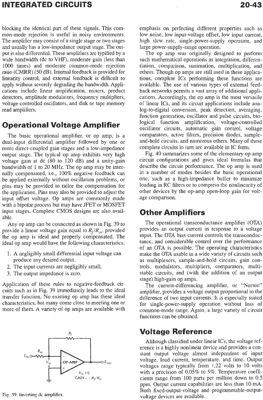
Static
RAM-Static RAMS are realized from a
memory cell with
a
bistable circuit.
A
simple flip-flop
is commonly used for the memory cell, as shown in
Fig.
37.
Note that
this
can be constructed with either
bipolar or MOS technology. The bipolar versions have
traditionally been faster than the
MOS
versions. How-
ever, the bit density of
MOS
sRAMs
has been larger
than for bipolar versions. The important elements of the
cell are the load (M,, M2) and the cross-coupled driver
(A)
NMOS
OXIDE
FLOATING
OXIDE
CONTROL GATE
EC
EF
EV
FLOATING GATE
(€3)
Flootlng
gate
Fig.
36.
Transistors
for
EPROM and EEPROM
memories.
20-42
REFERENCE DATA
FOR
ENGINEERS
WORD
I
"r
1
BIT
I
-
BIT
Fig.
37.
A
static
RAM
cell.
devices
(M3,
M4) that form the bistable latch. The
access transistors
(M5,
M6)
are used to address the cell.
The major considerations in the design of an
sRAM
cell are power, speed, and data hold. The power in the
cell is proportional to the load current. The load ele-
ment has been realized
as
a depletion MOSFET in
4K-
bit memories. However, it has been replaced by high-
impedance resistors realized by undoped polysilicon,
or by subthreshold current
in
a
short-channel MOSFET,
for higher-density memories. The
sRAM
cell with low-
est power is realized from complementary
MOS
tech-
nology. These memories can hold data with extremely
low power
(50-1000
nW)
and are being used with bat-
teries as low-cost alternatives to nonvolatile memories
in
some systems. Because of the large number of ele-
ments and connections to the memory cell, static
RAMs
tend to be lowest in bit density per chip among
semiconductor memories. However, the differential cell
provides a large signal-to-noise ratio and very high-
speed operation. Bipolar memories are all static and
have demonstrated access times below
10
ns.
Dynamic
RAM-Dynamic RAMs are constructed
commercially with MOS technology only, and they
represent the largest-volume, most widely used semi-
conductor memory. The memory is physically realized
by
the
storage of charge
on
an
MOS
capacitor that is
accessed by a MOSFET, as shown schematically in
Fig.
38.
The data bit is stored
as
a
charge packet
on
the
MOS
capacitor. Since the
MOS
capacitor is not an
ideal element and has nonzero leakage, it is discharged
through these leakage mechanisms
as
a
function of
time. The design of dynamic
RAMs
is thus critically
dependent
on
the reduction of leakage in the
MOS
capacitor. This requires
the
realization of very long
carrier lifetimes in the semiconductor and very high
crystalline quality. The signal-to-noise ratio depends
on
the ratio of the storage capacitor to the capacitance
of
the digit or bit line on which the charge
is
dumped
when the cell is accessed.
As
the bit density per chip
grows, this ratio is degraded, since the cell area is
WORD
LINE
4
Fig.
38.
The
one-transistodcapacitor
dRAM
cell.
decreased and more cells are added
on
the bit lime.
It
is
thus important
to
store
as
high
a
voltage as possible
on
the cell capacitor and increase its capacitance per unit
area
as
much as possible. The sensing
of
this
small sig-
nal is one of the most difficult circuit design problems,
and rather elaborate dynamic circuit techniques have
been developed for the purpose.
New Developments
The growth of all the above-described memories
following the scaling
of
MOSFET technology is
on
an
evolutionary path. The state-of-the-art memories in the
development stage include
up
to
2
gigabits
of
ROM
and
2
gigabits of dynamic
RAM.
The memory market
for all sectors except static
RAM
has been dominated
by
MOS
technology and will continue to be
so.
How-
ever, the bipolar memories have had
a
strong edge in
speed in the past. One-micron
MOS
static
RAMs
are
speed-competitive with bipolar memories. However,
the bipolar memories are significantly more radiation
hard and will tend to have major applications
in
hostile
environments.
LINEAR INTEGRATED
CIRCUITS*
Unlike digital integrated circuits, which respond to
and produce two-state logic signals, linear
ICs
give an
output signal that can be made to vary linearly with
respect
to
a varying input signal. Since linear
ICs
can
be used in
a
variety
of
applications and new designs
appear regularly, standardization
of
circuit elements as
in the case of digital
ICs
is impractical. Several impor-
tant families of linear
ICs
have evolved. They include
the device categories described below. The various
manufacturers' data books and applications books
should be consulted for detailed information.
Differential Amplifier
The basic differential amplifier consists of two identi-
cal input transistors connected to respond to the differ-
ence between two input signals while simultaneously
*
References 23,24,25,26,
and
27.
INTEGRATED CIRCUITS
20-43
blocking the identical part of these signals.
This
com-
mon-mode rejection is useful in noisy environments.
The amplifier may consist of a single stage or two stages
and usually has a low-impedance output stage. The out-
put
is
also differential. These amplifiers
are
typified by a
wide bandwidth (dc to
VHF),
moderate gain (less than
1000
times) and moderate common-mode rejection
ratio (CMRR)
(50
dB). Internal feedback is provided for
linearity control, and external feedback is difficult to
apply without severely degrading the bandwidth. Appli-
cations include linear amplification, mixers, product
detectors, amplitude modulators, frequency multipliers,
voltage-controlled oscillators, and disk or tape memory
read amplifiers.
0
pe ra
t
i
o
na
I
Vo
I
tag
e
Am p
I
if
i
e r
The basic operational amplifier, or op amp, is a
dual-input differential amplifier followed by one or
more direct-coupled gain stages and a low-impedance
output stage. The typical op amp exhibits very high
voltage gain at dc
(80
to
120
dB) and a unity-gain
bandwidth of
1
to 20 MHz. The op amp may be inter-
nally compensated, i.e., 100% negative feedback can
be applied externally without oscillation problems, or
pins may be provided to tailor the compensation for
the application. Pins may also be provided to adjust the
input offset voltage. Op amps are commonly made
with a bipolar process but may have JFET or MOSFET
input stages. Complete CMOS designs are also avail-
able.
Any op amp can be connected as shown in Fig. 39 to
provide a linear voltage gain equal to
R&,,
provided
the op amp is ideal and properly compensated. The
ideal op amp would have the following characteristics:
1.
A negligibly small differential input voltage can
produce any desired
output.
2.
The input currents are negligibly small.
3.
The output impedance is zero.
Application of these rules to negative-feedback cir-
cuits such as in Fig. 39 immediately leads to the ideal
transfer function.
No
existing op amp has these ideal
characteristics, but many come close
to
meeting one or
more of them. A variety of op amps are available with
GAIN
=
-
R,/R,,
L
Fig.
39.
Inverting dc
amplifiet.
emphasis
on
perfecting different properties such as
low noise, low input-voltage offset, low input current,
high slew rate, single-power-supply operation, and
large power-supply-range operation.
The op amp was originally designed to perform
such mathematical operations as integration, differen-
tiation, comparison, summation, multiplication, and
others. Though op amps are still used in these applica-
tions, complete
ICs
performing these functions are
available. The
use
of various types of external feed-
back networks permits a vast array of additional appli-
cations. Accordingly, the op amp is the most versatile
of linear ICs, and its circuit applications include ana-
log-to-digital conversion, peak detection, averaging,
function generation, oscillator and pulse circuits, bio-
logical function amplification, voltage-controlled
oscillator circuits, automatic gain control, voltage
comparators, active filters, precision diodes, sample-
and-hold circuits, and numerous others. Many of these
complete circuits in turn are available
in
IC form.
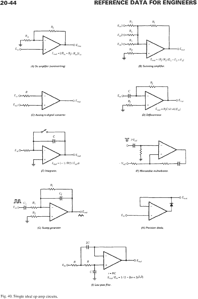
Fig.
40
summarizes some of the elementruy op-amp
circuit configurations and gives ideal formulas that
describe the circuit performance. The op amp is used
in a number of modes besides the basic operational
one, such as a high-impedance buffer to minimize
loading in RC filters or to compress the nonlinearity of
other devices by the op-amp open-loop gain for volt-
age comparison.
Other Amplifiers
The operational transconductance amplifier (OTA)
provides an output current in response to a voltage
input. The OTA bias current controls the transconduc-
tance, and considerable control over the performance
of an
OTA
is possible. The operating characteristics
make the OTA usable
in
a wide variety of circuits such
as multiplexers, sample-and-hold circuits, gain con-
trols, modulators, multipliers, comparators, multi-
stable circuits, and (with the addition of an output
stage) high-gain op amps.
The current-differencing amplifier, or
“Norton”
amplifier, provides a voltage output proportional to the
difference of two input currents. It is especially suited
for single-power-supply operation without loss of
common-mode range. Again, a large variety of circuit
functions can be obtained.
Voltage Reference
Although classified under linear ICs, the voltage ref-
erence is a highly nonlinear device and provides a con-
stant output voltage almost independent of input
voltage, load current, temperature, and time. Output
voltages range typically from 1.22 volts to
10
volts
with a precision of
0.05%
to
5%.
Temperature coeffi-
cients range from
100
parts per million down to
0.5
ppm. Output current capabilities are less than 10 mA.
Both fixed-output-voltage and programmable-output-
voltage devices are available.
20-44
REFERENCE
DATA
FOR ENGINEERS
(A)
Dc
ornpllfler (nonlnverting)
(C)
Analog-to-dlglml converter
(E)
Integrator.
(G)
Sweep generotor
R1
R'
(B)
Surnrnlng ornpliper.
(Dl Dlfferentiotor
(F)
Monostable rnultiuibmtor
(H)
Precision dlode
A
€o"I/€,n=l/(l
+2ST+2S272)
(I)
Low-pass filter
Fig.
40.
Simple ideal
op-amp
circuits.
INTEGRATED CIRCUITS
20-45
Reference diodes also come in IC form and simulate
the characteristic of a zener diode, but with a much
sharper breakdown characteristic.
Some applications are amplifier biasing for temper-
ature independence, constant-cun-ent-source circuits,
level detectors, and low-voltage regulators.
Voltage Regulators
Bipolar voltage-regulator ICs incorporate a voltage
reference and a sense amplifier and maintain the
out-
put voltage at a value almost independent of load,
input voltage and ripple, and temperature. Both fixed-
and programmable-output-voltage units are made.
Voltages up to
50
volts can be regulated. Current capa-
bility is usually
on
the order of tens of milliamperes,
and the IC is intended as the driver for large-pass tran-
sistors that can accommodate the higher currents and
operating temperatures that occur in power supplies.
External components for current limiting, noise reduc-
tion, and compensation are desirable additions in the
design
of
a complete power supply.
Comparators
The voltage comparator is a differential amplifier
design with a small delay time between the application
of a differential input signal and the output transition.
The output swing is made compatible with TTL inputs.
Emphasis is placed
on
low-input bias current and its
offset and low-input offset voltage, and the usual
amplifier specifications are of lesser importance. Com-
mon applications are high-speed analog-to-digital con-
verters, fast zero-crossing detectors, tape- and disk-file
read channels, and differential line receivers.
Special-Purpose Linear
Integrated Circuits
Since any circuit that can be assembled from dis-
crete semiconductor components can almost always be
duplicated or simulated with monolithic IC technol-
ogy, a great many special-purpose ICs exist. These
include custom designs for use in various kinds of
commercial products as well as a wide range of off-
the-shelf numbered units. The commercial units
include such devices as music synthesizers, phase-
locked loops, tone decoders and encoders, function
generators, programmable filters,
FM
and video
demodulators,
IF
detectors, subcamer regenerators,
AGC, FM stereo demultiplexers, AM-receiver func-
tional blocks, timers, audio and power amplifiers, volt-
age-to-frequency converters, analog-to-digital and
digital-to-analog converters, instrumentation amplifi-
ers, and sample-and-hold circuits.
Though many of the ICs are dedicated to a specific
application or function, the addition of a few external
components can often result
in
a wide range of addi-
tional applications. The list of special-purpose linear
ICs grows constantly, and the design engineer is well
advised to consult current manufacturers’ data and
application literature.
Miscellaneous Linear ICs
Other useful building blocks are timers, transistor-
diode arrays, digitally controlled analog pass-gates,
optical isolators, bar or dot LED-display drivers, and
analog shift registers.
TRENDS
IN
INTEGRATED
CIRCUITS
Sca
I
i
ng and
Mi
n iat
u
r izat
i
on
The explosive growth
of
integrated circuits has been
fueled by the ability to scale the minimum lithographic
dimensions of an integrated circuit. This results in a
threefold advantage:
1.
Increase in density of circuit elements per chip
2.
Increase
in
circuit performance due to increased
device gain and reduced load capacitance
3.
Decrease in cost per function, which provides
economic incentive
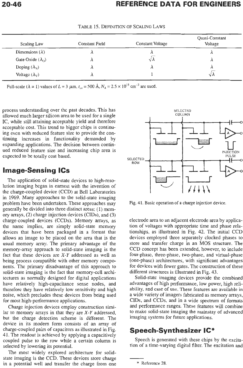
The most significant improvement in integration
complexity has been achieved in MOS circuits. An
exponential growth of the number of circuit elements
in time has been noted. This has been made possible
by the simple scaling laws that relate the scaling of
vertical and lateral dimensions to the scaling of doping
and voltages. Table
15
shows three sets
of
scaling laws
that have been used to various degrees. The first
assumes that the electric field in the device must be
held constant. The second is based
on
complying with
currently set voltage standards, and the third proposes
a change in the voltage standards only when the elec-
tric field is high enough
to
cause problems as the result
of secondary effects. Another scaling theory has been
proposed
on
the basis of the off-state switching behav-
ior of
MOS
devices. Scaling of bipolar devices does
not proceed along scaling laws because the base width
that is the critical dimension is much smaller than all
other dimensions. Scaling of bipolar technology
is
aimed at reduction
of
parasitic device capacitance.
Scaling of ICs has proceeded unabated for the past
two generations, despite several predictions along the
way that the “end of scaling is imminent.” These pre-
dictions proposed unbreakable roadblocks
along
the
way at minimum IC feature sizes of
1.0
micron,
0.5
micron,
0.25
micron, and smaller. In each case, inge-
nuity and hard work have overcome critical road-
blocks. At the present time, manufacturing is occurring
at 0.15-micron feature sizes, and 0.1-micron feature
sizes are fully anticipated in manufacturing
in
2005.
The “end of scaling” is still being predicted, but at fea-
ture sizes in the
.02
micron range.
Integration complexity in ICs has also benefited
greatly from improvements in process equipment and
20-46
REFERENCE
DATA
FOR ENGINEERS
TABLE 15. DEFINITION
OF
SCALING
LAWS
Quasi-Constant
Scaling Law Constant Field Constant Voltage Voltage
Dimensions
(A) A
A
A
Gate
Oxide
(A,)
Doping
(Ad
Voltage
(A,)
A
A
A
&
A
1
Full-scale
(A
=
1)
values
of
L
=
3
pm,
to,
=
500
A,
NA
=
2.5
x
lOI5
cm-3
are
used.
process understanding over the past decades. This has
allowed much larger silicon area to be used for a single
IC, while still attaining acceptable yield and therefore
acceptable cost. This trend to bigger chips is continu-
ing even with reduced feature size to provide the con-
tinuing increases in functionality demanded by
expanding applications. The decision between contin-
ued reduced feature size and increasing chip area is
expected to be totally cost based.
Image-Sensing
ICs
The application of solid-state devices
to
high-reso-
lution imaging began in earnest with the invention of
the charge-coupled device (CCD) at Bell Laboratories
in
1969.
Many approaches to the solid-state imaging
problem have been undertaken. These approaches may
generally be divided into three distinct areas:
(1)
mem-
ory arrays,
(2)
charge injection devices (CIDs), and
(3)
charge-coupled devices (CCDs). Memory arrays, as
the name implies, are simply solid-state memory
devices that have been packaged in a format that
allows an image to be placed on the area that is the
usual memory array. The primary advantage of the
memory-array approach
to
solid-state imaging is the
fact that these devices
are
X-Y
addressed as well as
being process compatible with other memory compo-
nents. The primary disadvantage of this approach
to
solid-state imaging is the fact that memory-cell archi-
tectures as normally designed for digital applications
have relatively high-capacitance sense nodes, and
therefore they have relatively low sensitivity and high
noise, which precludes these devices from being used
for most high-performance applications.
Charge injection devices employ construction simi-
lar to memory arrays in that they are
X-Y
addressed,
but the charge detection scheme is different. The
device in its modem form consists of an array of
charge-coupled pairs of capacitors as illustrated in Fig.
41.
The readout is achieved by applying a capacitively
coupled pulse to the row while a certain column is
selected by lowering its potential.
The most widely explored architecture for solid-
state imaging is the CCD. These devices store charge
in a potential well and transfer the charge from one
SELECTED
COLUMN
U
INJECTION
PULSE
SELECTED
I
-
I
il+\i
Fig.
41.
Basic operation
of
a charge injection device.
electrode area to an adjacent electrode area by applica-
tion of voltages with appropriate time and phase rela-
tionships, as illustrated in Fig.
42.
The initial CCD
devices employed three separately clocked phases to
store and transfer charge in an MOS structure. The
CCD concept has been extended, however, to include
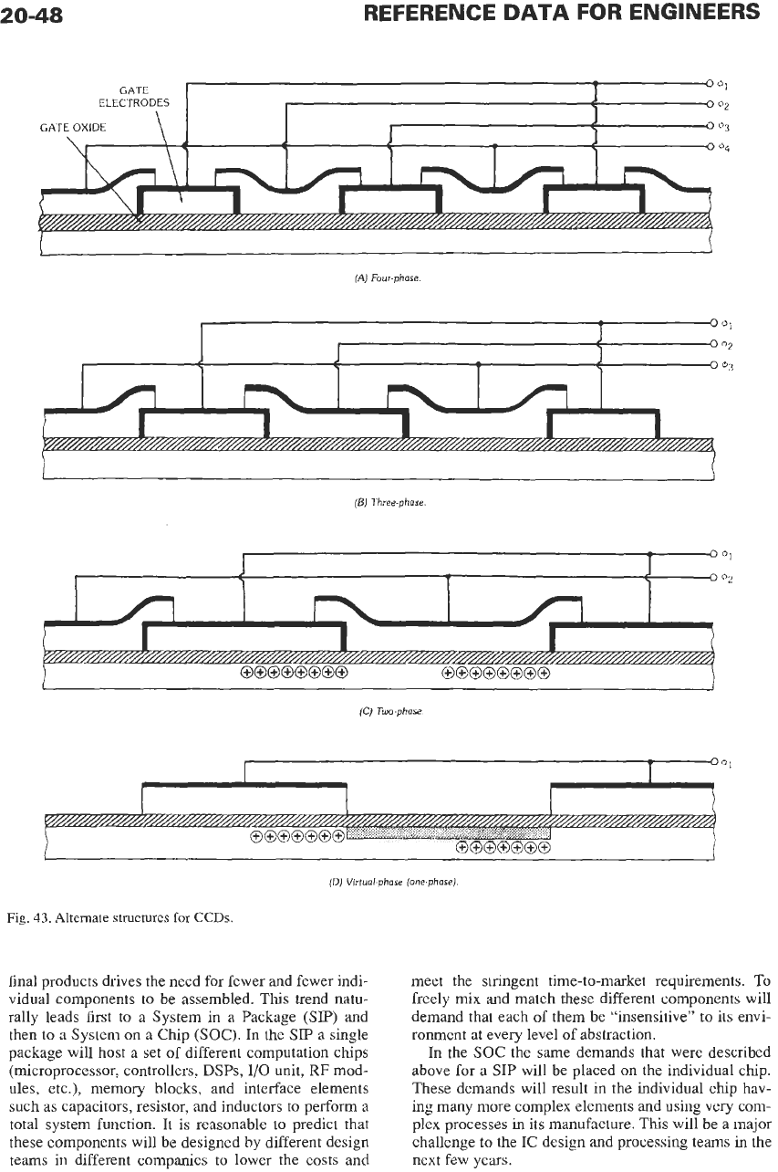
four-phase, three-phase, two-phase, and virtual-phase
(one-phase) architectures, with significant advantages
for devices with fewer gates. The construction of these
different structures is illustrated
in
Fig.
43.
Solid-state imaging devices provide the combined
advantages
of
high performance, low power, high reli-
ability, and ease of use. These features are available
in
a wide variety of imagers fabricated as memory arrays,
CIDs, and CCDs, and in a wide spectrum
of
formats
and performance ranges. These features will combine
to make solid-state imaging the mainstay of advanced
imaging systems for future applications.
Speech-Synthesizer IC*
Speech is generated with these chips by the excita-
tion of a time-varying digital filter. The excitation and
*
Reference
28
INTEGRATED CIRCUITS
20-47
fl
:r.
..::.*:,:..:5.:::,:.:):8":f
8:.:::.~::.,.::~~:*.,:~:~
.....
........-.
:.:
.....
..-.....
:...-:.
...
p3
CLOCK
11
fP
f3
I4
I5
f6
fl
Fig.
42.
Basic operation
of
a charge-coupled device.
filter parameters are stored in
ROM, EPROM, RAM,
or disk memory or are generated by a program. Overall
control is provided by a microprocessor. The process is
entirely digital up to the analog-to-digital converter,
which provides the analog signal to drive a speaker.
An
alternative to the variable-filter approach is to
store digitized speech and sample the data at an 8-kHz
rate, which leads to a digital data rate of about
100
kHz.
Logarithmically compressed amplitude data
could be used, analogous to digital telephone systems,
which results in a rate of
64
kilobits/second with very
good quality. The time-varying filter techniques pro-
vide acceptable speech quality but at a much lower
digital input data rate, down to an average rate
of
1200
bits/second for a ten-pole filter derived from a linear
prediction model of speech.
The low data rates are made possible because of the
redundancy
in
speech and by using a simplified simu-
lator of the human speech-generating system. The
vocal tract is simulated by a dozen or
so
connected
pipes
of
differing diameter, and the excitation is repre-
sented by a pulse stream at the vocal-chord rate for
voiced sound or by a random noise source for the
unvoiced parts
of
speech. The reflection coefficients at
the junctions of the pipes can be obtained from a linear
prediction analysis of the speech waveform, and the
names associated with the
ICs,
such as LPC or
PAR-
COR,
refer to the particular analysis used to obtain the
coefficients for the equivalent electrical digital filter.
System in a Package (SIP) and
System on a
Chip
(SOC)
As
ICs
continue to become pervasive in consumer
applications, the need for smaller size and lower cost
20-48
REFERENCE
DATA
FOR ENGINEERS
ELECTRODES
GATEOXIDE
\
I
(A)
Four.phase
(BJ
Three-phase.
I
1
Q
*I
1
1
-i
(Cj
Two-phase.
Fig.
43.
Alternate
structures
for
CCDs.
final products drives the need for fewer and fewer indi-
vidual components
to
be assembled.
This
trend natu-
rally leads first to
a
System in
a
Package (SIP) and
then to a System on a Chip (SOC). In the
SIP
a single
package will host
a
set of different computation chips
(microprocessor, controllers, DSPs, I/O unit,
RF
mod-
ules, etc.), memory blocks, and interface elements
such as capacitors, resistor, and inductors to perform
a
total system function. It is reasonable to predict that
these components will be designed by different design
teams in different companies to lower the costs and
meet the stringent time-to-market requirements.
To
freely mix and match these different components will
demand that each of them be “insensitive”
to
its envi-
ronment at every level
of
abstraction.
In the
SOC
the same demands that were described
above
for
a
SIP
will be placed on the individual chip.
These demands will result in the individual chip hav-
ing many more complex elements and using very com-
plex processes
in
its manufacture.
This
will be a major
challenge
to
the IC design and processing teams in the
next few years.
Micro-Electro-Mechanical
Systems
(MEMS)
Micro-Electro-Mechanical
Systems (MEMS) are
integrated mechanical elements, sensors, actuators,
and electronics that are fabricated using microfabrica-
tion technology similar to that used for integrated cir-
cuits.
In
most
cases MEMS exist on a common silicon
substrate; however, MEMS can be combined as dis-
crete microcomponents in a single package. While
MEMS
electronics are fabricated using
IC
process
materials and process sequences, many times the
micromechanical components, sensors, and actuators
are fabricated using compatible “micromachining”
processes that deposit new layers or selectively etch
away parts of the silicon wafer to form the mechanical
and electromechanical devices. MEMS devices that
are manufactured using batch fabrication techniques
like those used for
ICs
provide the outstanding levels
of functionality, reliability, and sophistication that
have been demonstrated on
ICs,
with the coupled
advantage of relatively low cost.
MEMS have emerged as significant contenders
to
satisfy the needs of several major existing and emerg-
ing markets. Probably the most familiar application to
the
IC
industry is in the MEMS accelerometers that are
quickly replacing conventional accelerometers for air-
bag deployment systems in automobiles. The conven-
tional approach uses several bulky accelerometers
made of discrete components mounted in the front
of
the car with separate electronics near the
air
bag.
MEMS have made it possible
to
integrate the acceler-
ometer and electronics onto a single silicon chip at a
cost that is a factor of 10 below the mechanical coun-
terpart.
A
second application that is receiving signifi-
cant publicity is the
TI
DMD device that is used in
projection displays. The high resolution and brightness
provided for this application, combined with the low
cost and ease of transport and modification of digital
data, promises
to
revolutionize the movie and commer-
cial display markets.
A
third MEMS application that
has a major market potential is in optical switching.
The recent emphasis
on
expanded optical communica-
tions to meet the requirements of wireless communica-
tions and the Internet is driving a wave of need for
high-density, low-power, low-cost optical switches.
This need is being met by the micromechanical optical
switch, which is expected
to
serve a major market in
the future.
In
addition to the applications noted above,
MEMS
are appearing in a multitude of special applica-
tions in such diverse fields as health care, metrology
systems, defense, and space science applications.
APPLICATION SPECIFIC
INTEGRATED CIRCUITS*
One of the fastest growing semiconductor market
sectors is application specific integrated circuits (com-
*
This
section
was
contributed
by
Mark
G.
Harward.
monly referred to as
ASICs).?
The increasing use of
ASICs
continues
to
be market driven by the rapid
advance
of
technology, which has shortened the useful
life of most electronic products as improved and less
expensive products make existing models quickly
obsolete.$ Furthermore, because most of the profit
from electronic systems is earned early in the product
life cycle, the penalty for being late to market is
severe. The time required to design, manufacture pro-
totype systems, and perform design revisions with
ASICs
is much less than with full-custom integrated
circuits.
ASICs
are cost-effective solutions for all but
the very highest volume products in which the smaller
chip size of full custom design and layout can offset
the advantages of
ASICs
if the product life is suffi-
ciently long. The next paragraphs describe the major
classes
of
ASICs,
and then anticipated future trends in
ASICs
are discussed. The use of
ASICs
rather than
“off-the-shelf” standard logic parts is also influenced
by
ASIC
benefits such as reduced cost and size, and
improved reliability resulting from higher levels of
integration
so
that fewer system components are
required. Systems based on proprietary
ASICs
are also
much more difficult to replicate by competitors.
Gate Arrays
Gate arrays are the largest single
ASIC
market seg-
ment.# They offer a good balance of cost, capability,
time to initial silicon, and performance.
A
gate array
is
a chip from a master slice in which the active devices
are regular arrays of digital logic “base cells” that can
be interconnected into numerous types of simple and
complex logic gates or sequential elements. The
designer selects elements from a set of functional cir-
cuit blocks called the “macro library.” Master slices
are semiconductor wafers that have been fabricated
through much of the
IC
process
so
that all active
devices are present, though not yet connected by the
metal layers.
An
inventory of wafers is built to provide
manufacturing economies
of
scale; then the custom
interconnect layers are patterned as orders are
received.
There are two primary gate-array architectures:
channelled and sea-of-gates. Channelled architectures
disallow the use of selected rows and/or columns of
base cells to use those regions as channels for the hori-
zontal and/or vertical routing of signals and power
supplies (Fig.
44).
Triple-level metallization process
technology has enabled the sea-of-gates architecture
to begin replacing channelled gate arrays for higher-
density applications that require more gates. With
three interconnect layers, routing over utilized base
cells is possible without setting aside channels. “Gate
utilization” is a term that describes the percentage of
t
References
29,30,
and
31
$
References
32
and
33.
§
Reference
29.