Middleton W.M. (ed.) Reference Data for Engineers: Radio, Electronics, Computer and Communications
Подождите немного. Документ загружается.

20-50
REFERENCE
DATA
FOR ENGINEERS
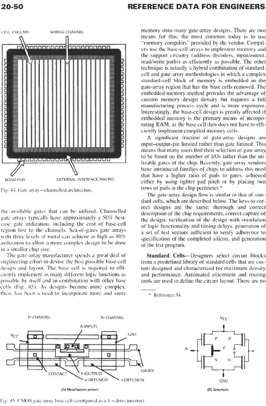
CELL
COLUMN WIRING CHANNEL
BOND
PAD
EXTERNAL INERFACE MACRO
Fig.
44.
Gate array-channelled architecture.
the available gates that can be utilized. Channelled
gate arrays typically have approximately a
50%
best-
case gate utilization, including the cost of base-cell
region lost to the channels. Sea-of-gates gate arrays
with three levels of metal can achieve as high as
80%
utilization to allow a more complex design to
be
done
in a smaller chip size.
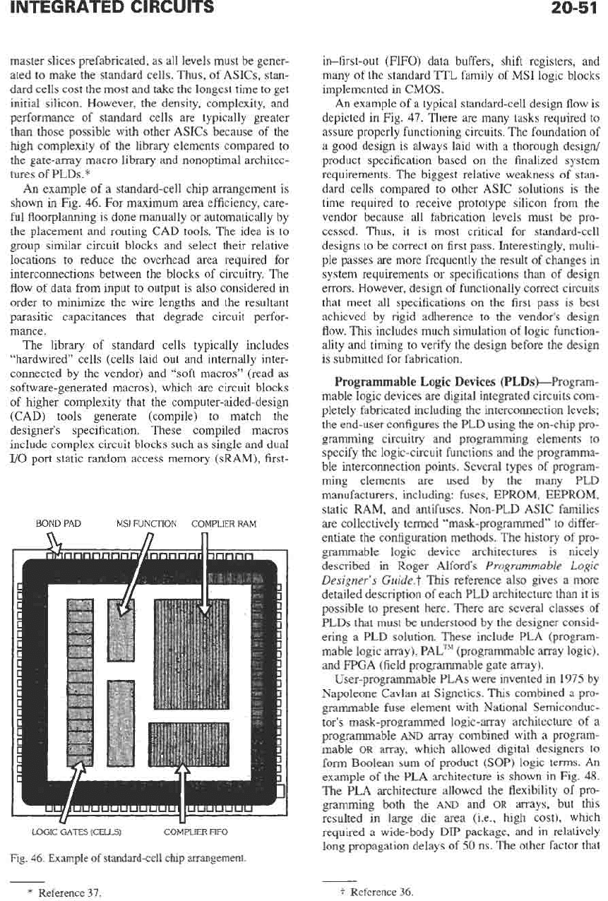
The gate-array manufacturer spends a great deal of
engineering effort to devise the best possible base-cell
design and layout. The base cell is required to effi-
ciently implement as many different logic functions as
possible by itself and in combination with other base
cells (Fig.
45).
As
designs become more complex,
there has been a need to incorporate more and more
P-CHANNEL N-CHANNEL
AWW
(A)
Merallllotlm
pattern
Fig.
45.
CMOS
gate-array base cell (configured as a
1
x
drive
inverter).
memory onto many gate-array designs. There
are
two
means for this; the most common today is to use
“memory compilers” provided by the vendor. Compil-
ers use the base-cell arrays to implement memory and
the support circuitry (address decoders, inputjoutput,
read/write paths) as efficiently
as
possible. The other
technique
is
actually a hybrid combination of standard-
cell and gate-array methodologies in which
a
complex
standard-cell block of memory
is
embedded in the
gate-array region that has the base cells removed. The
embedded-memory method provides the advantage of
custom memory design density but requires a full
manufacturing process cycle and is more expensive.
Interestingly,
the
base-cell design is greatly affected if
embedded memory is the primary means of incorpo-
rating
RAM,
as
the base cell then does not have to effi-
ciently implement compiled memory cells.
A
significant fraction
of
gate-array designs
are
input-output-pin limited rather than gate limited.
This
means that many users find their selection of gate array
to
be
based
on
the number of
I/Os
rather than the uti-
lizable gates of
the
chip. Recently, gate-array vendors
have introduced families of chips to address
this
need
that have a higher ratio of pads to gates, achieved
either by using tighter pad pitch
or
by placing
two
rows of pads at the chip perimeter.*
The gate-array design flow is similar to that of stan-
dard cells, which
are
described below. The keys
to
cor-
rect designs
are
the
same: thorough and correct
description of
the
chip requirements, correct capture of
the design, verification of the design with simulation
of logic functionality and timing delays, generation of
a set of test vectors sufficient to verify adherence to
specification of
the
completed silicon, and generation
of
the test program.
Standard
Cells-Designers select circuit blocks
from a predefined library of standard cells that
are
cus-
tom designed and characterized for maximum density
and performance. Automated placement and routing
tools
are
used to define the circuit layout. There are no
*
Reference
34.
INTEGRATED
CIRCUITS
20-5
1
master slices prefabricated, as all levels must be gener-
ated to make the standard cells.
Thus,
of ASICs, stan-
dard cells cost the most and take the longest time
to
get
initial silicon. However, the density, complexity, and
performance of standard cells are typically greater
than those possible with other ASICs because
of
the
high complexity of the library elements compared to
the gate-array macro library and nonoptimal architec-
tures of PLDs.”
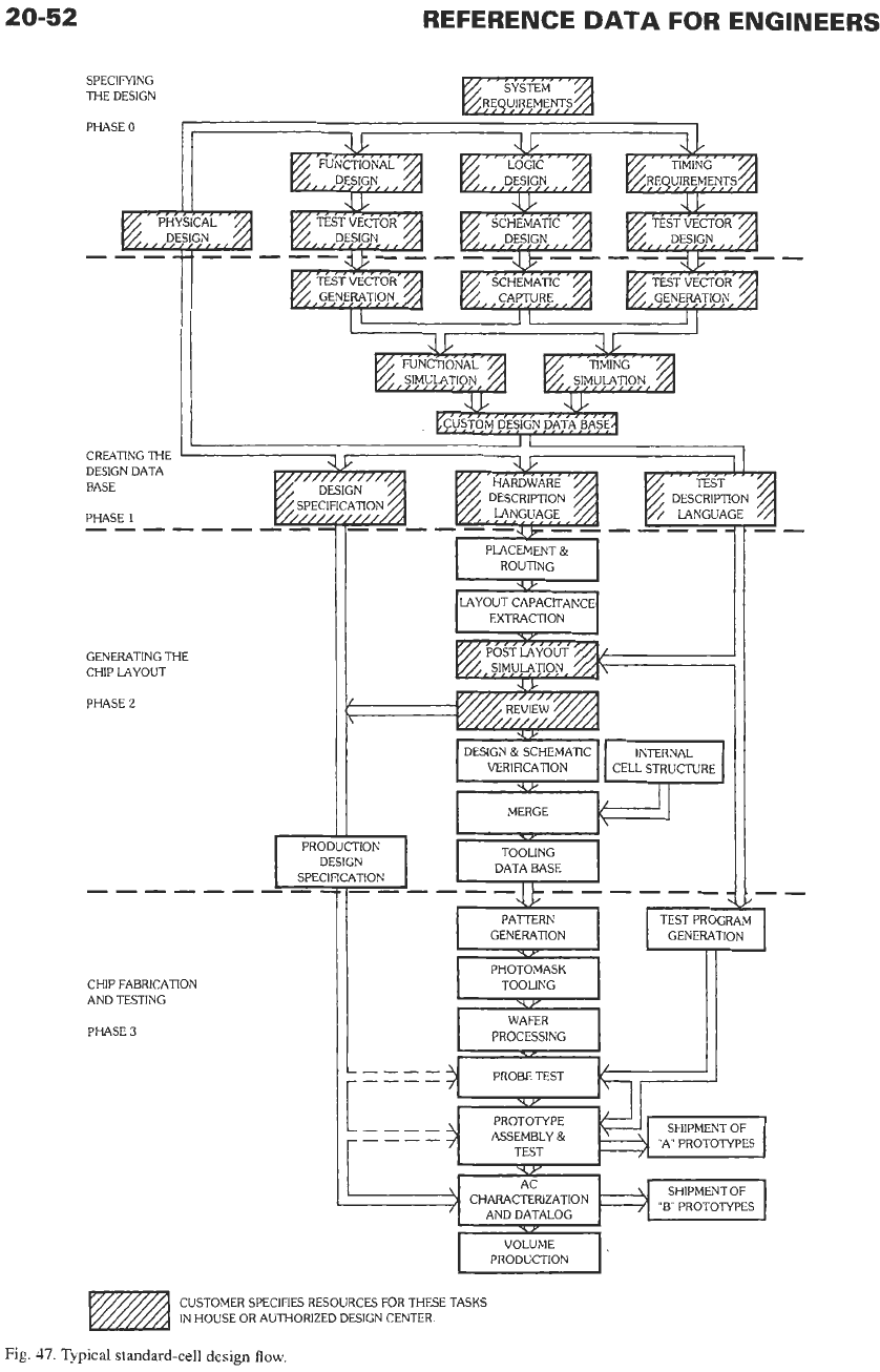
An example of a standard-cell chip arrangement is
shown in Fig.
46.
For maximum area efficiency, care-
ful floorplanning is done manually or automatically by
the placement and routing CAD tools. The idea is
to
group similar circuit blocks and select their relative
locations to reduce the overhead area required for
interconnections between the blocks of circuitry, The
flow of data from input to output is also considered in
order to minimize the wire lengths and the resultant
parasitic capacitances that degrade circuit perfor-
mance.
The library of standard cells typically includes
“hardwired” cells (cells laid out and internally inter-
connected by the vendor) and “soft macros” (read as
software-generated macros), which are circuit blocks
of higher complexity that the computer-aided-design
(CAD) tools generate (compile) to match the
designer’s specification. These compiled macros
include complex circuit blocks such as single and dual
1/0
port static random access memory (sRAM), first-
BOND PAD
MSI
FUNCTION COMPLIER RAM
LOGIC GATES
(CELLS)
COMPLIER
FIFO
Fig.
46.
Example
of
standard-cell chip
arrangement
*
Reference
37.
in-first-out (FIFO) data buffers, shift registers, and
many
of
the standard TTL family of MSI logic blocks
implemented
in
CMOS.
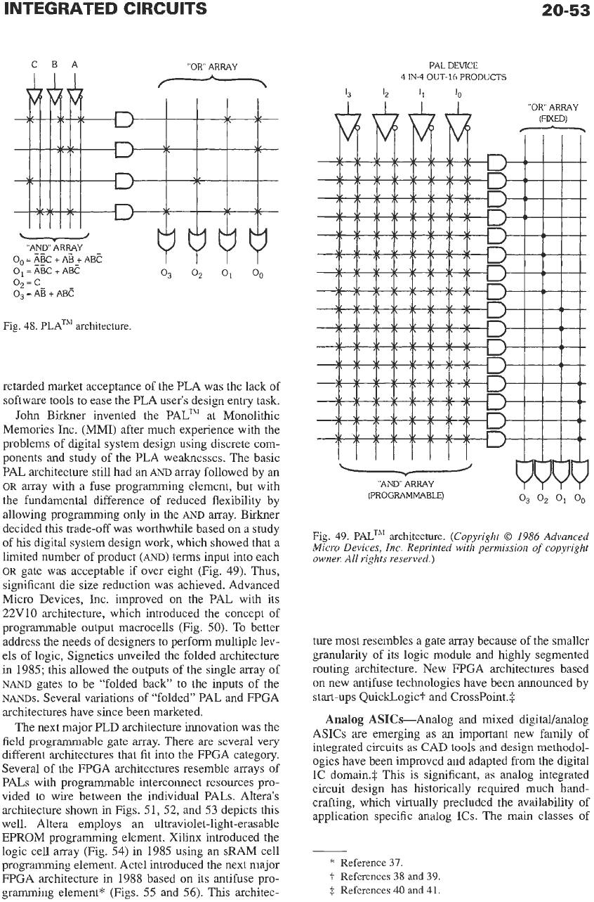
An
example of a typical standard-cell design flow is
depicted in Fig.
47.
There are many tasks required to
assure properly functioning circuits. The foundation of
a good design is always laid with a thorough design/
product specification based on the finalized system
requirements. The biggest relative weakness of stan-
dard cells compared to other ASIC solutions is the
time required to receive prototype silicon from the
vendor because all fabrication levels must be pro-
cessed.
Thus,
it is most critical for standard-cell
designs
to
be correct on first pass. Interestingly, multi-
ple passes are more frequently the result of changes in
system requirements or specifications than of design
errors. However, design of functionally correct circuits
that meet all specifications
on
the first pass is best
achieved by rigid adherence to the vendor’s design
flow. This includes much simulation of logic function-
ality and timing to verify the design before the design
is submitted for fabrication.
Programmable Logic Devices
(PLDsrProgram-
mable logic devices are digital integrated circuits com-
pletely fabricated including the interconnection levels;
the end-user configures the PLD using the on-chip pro-
gramming circuitry and programming elements to
specify the logic-circuit functions and the programma-
ble interconnection points. Several types
of
program-
ming elements are used by the many PLD
manufacturers, including: fuses, EPROM, EEPROM,
static RAM, and antifuses. Non-PLD ASIC families
are collectively termed “mask-programmed” to differ-
entiate the configuration methods. The history of pro-
grammable logic device architectures is nicely
described in Roger Alfords
Programmable Logic
Designer’s Guide.t
This reference also gives a more
detailed description of each PLD architecture than it is
possible to present here. There are several classes of
PLDs that must be understood by the designer consid-
ering a PLD solution. These include PLA (program-
mable logic array), PAL’” (programmable array logic),
and FPGA (field programmable gate array).
User-programmable PLAs were invented in
1975
by
Napoleone Cavlan at Signetics. This combined a pro-
grammable fuse element with National Semiconduc-
tor’s mask-programmed logic-array architecture of a
programmable
AND
array combined with a program-
mable
OR
array, which allowed digital designers
to
form Boolean sum of product (SOP) logic terms.
An
example of the PLA architecture is shown in Fig.
48.
The PLA architecture allowed the flexibility of pro-
gramming both the
AND
and
OR
arrays, but this
resulted in large die area (i.e., high cost), which
required a wide-body
DIP
package, and in relatively
long propagation delays of
50
ns. The other factor that
f
Reference
36.
20-52
REFERENCE
DATA
FOR ENGINEERS
SPECIFYING
THE DESIGN
PHASE
0
CREATING THE
DESIGN DATA
BASE
PHASE
1
DESCRIPTION
______
GENERATING THE
CHIP LAYOUT
PHASE
2
PLACEMENT
&
ROUTING
*P
LAYOUT CAPACITANCE
EXTRACTION
DESIGN
&
SCHEMATIC INTERNAL
VERIFICATION CELL STRUCTURE
w
MERGE
DESIGN
PATTERN TEST PROGW
CHIP FABRICATION
AND TESTING
PHASE
3
GENERATION
PHOTOMASK
TOOLING
PROCESSING
GENERATION
PROBE TEST
YY
"A
PROTOTYPES
I
PROTOTYPE
ASSEMBLY
&
r----
d
TEST
II
I
.^
I
I
SHIPMENT
OF
HL
"B
PROTOTYPES
CHARACTERIZATION
AND DATALOG
VOLUME
I
PRODUCTION
I
CUSTOMER SPECIFIES RESOURCES FOR THESE TASKS
IN HOUSE OR AUTHORIZED DESIGN CENTER.
Fig. 47.
Typical
standard-cell design
flow.
INTEGRATED
CIRCUITS
20-53
CBA
"OR
ARRAY
*
"A)? ARRAY
0,
=
ABC
+
AB_+
ABC
02=c
0,
=
AB
+
AB?
0,
=
ABC
+
ABC
03
02
01
00
Fig. 48. PLATM architecture.
retarded market acceptance
of
the PLA was the lack of
software tools to ease the PLA user's design entry task.
John Birkner invented the PALTM at Monolithic
Memories Inc. (MMI) after much experience with the
problems of digital system design using discrete com-
ponents and study of the PLA weaknesses. The basic
PAL
architecture still had
an
AM)
array followed by an
OR
array with a fuse programming element, but with
the fundamental difference of reduced flexibility by
allowing programming only
in
the
AND
array. Birkner
decided this trade-off was worthwhile based
on
a study
of his digital system design work, which showed that a
limited number of product
(AND)
terms input into each
OR
gate was acceptable if over eight (Fig. 49).
Thus,
significant die size reduction was achieved. Advanced
Micro Devices, Inc. improved
on
the PAL with its
22V10 architecture, which introduced the concept of
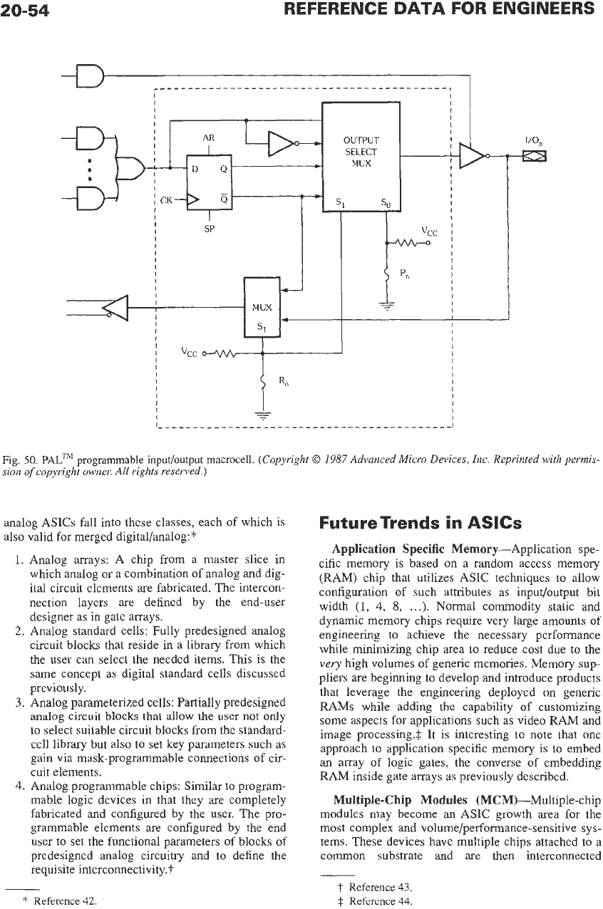
programmable output macrocells (Fig. 50).
To
better
address the needs of designers to perform multiple lev-
els of logic, Signetics unveiled the folded architecture
in 1985; this allowed the outputs of the single array of
NAND
gates
to
be "folded back"
to
the inputs of the
NANDS.
Several variations of "folded" PAL and FPGA
architectures have since been marketed.
The next major PLD architecture innovation was the
field programmable
gate
array. There are several very
different architectures that fit into the FPGA category.
Several of the FPGA architectures resemble arrays of
PALs with programmable interconnect resources pro-
vided
to
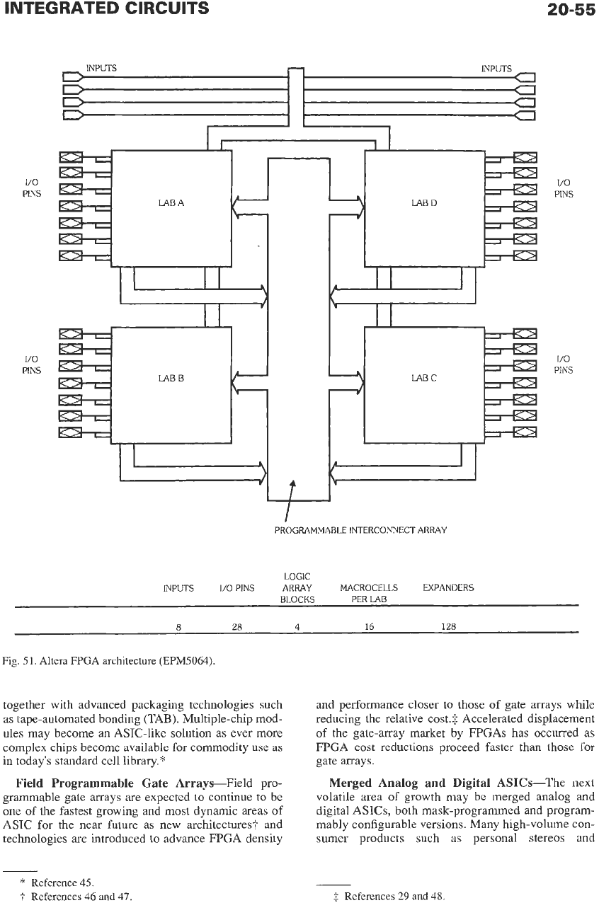
wire between the individual PALs. Altera's
architecture shown in Figs. 51, 52, and 53 depicts this
well. Altera employs an ultraviolet-light-erasable
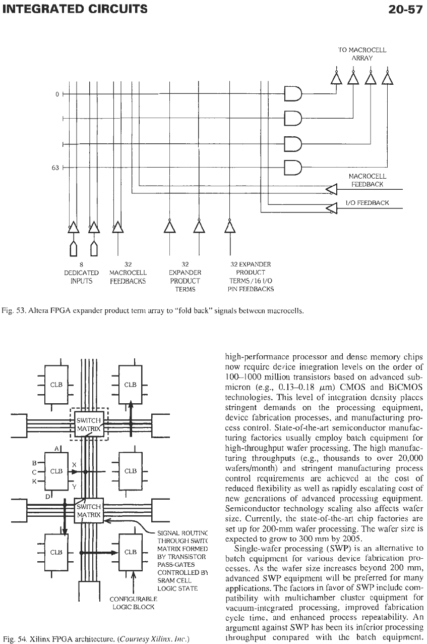
EPROM programming element. Xilinx introduced the
logic cell array (Fig. 54)
in
1985 using an sRAM cell
programming element. Actel introduced the next major
FPGA architecture in 1988 based
on
its antifuse pro-
gramming element* (Figs.
55
and
56).
This architec-
PAL
DEVICE
4
IN-4
OUT-16
PRODUCTS
13
'2
4
10
I I
I I
"OR
ARRAY
03
02
01
00
(PROGRAMMABLE)
Fig. 49.
PKTh'
architecture.
(Copyright
0
1986
Advanced
Micro Devices,
Inc.
Reprinted with permission
of
copyright
ownel:
All
rights reserved.)
ture most resembles a gate array because of the smaller
granularity of its logic module and highly segmented
routing architecture. New FPGA architectures based
on
new antifuse technologies have been announced by
start-ups QuickLogict and CrossPoint.$
Analog
ASIC-Analog and mixed digitalhalog
ASICs
are emerging as
an
important new family of
integrated
circuits
as
CAD
tools and design methodol-
ogies have been improved and adapted from the digital
IC domain.$ This is significant, as analog integrated
circuit design has historically required much hand-
crafting, which virtually precluded the availability of
application specific analog ICs. The main classes of
*
Reference
37.
7
References
38
and 39.
$
References
40
and
41.
REFERENCE
DATA
FOR ENGINEERS
j
I
"cc
0-m-
I I I
,
Fig.
50. PALTM
programmable
inputfoutput
macrocell.
(Copyright
0
1987
Advanced Micro Devices, Inc. Reprinted with pernzis-
sion
of
copyright owner.
All
rights resewed.)
analog ASICs fall into these classes, each
of
which is
also valid for merged digitalhalog:"
1.
Analog arrays: A chip from a master slice in
which analog or a combination
of
analog and dig-
ital circuit elements are fabricated. The intercon-
nection layers are defined by the end-user
designer as in gate arrays.
2.
Analog standard cells: Fully predesigned analog
circuit blocks that reside in a library from which
the user can select the needed items.
This
is the
same concept as digital standard cells discussed
previously.
3.
Analog parameterized cells: Partially predesigned
analog circuit blocks that allow the user not only
to select suitable circuit blocks from the standard-
cell library but
also
to set key parameters such as
gain via mask-programmable connections of cir-
cuit elements.
4.
Analog programmable chips: Similar to program-
mable logic devices in that they are completely
fabricated and configured by the user. The pro-
grammable elements are configured by the end
user
to
set the functional parameters of blocks of
predesigned analog circuitry and to define the
requisite interconnectivity.?
FutureTrends
in
ASKS
Application Specific Memory-Application spe-
cific memory is based on a random access memory
(RAM) chip that utilizes ASIC techniques
to
allow
configuration of such attributes as input/output bit
width
(1,
4,
8,
...).
Normal
commodity static and
dynamic memory chips require very large amounts of
engineering
to
achieve the necessary performance
while minimizing chip area to reduce cost due to the
very
high volumes
of
generic memories. Memory sup-
pliers are beginning to develop and introduce products
that leverage the engineering deployed
on
generic
RAMS while adding the capability
of
customizing
some aspects for applications such
as
video
RAM
and
image processing.?: It is interesting to note that one
approach to application specific memory is to embed
an array of logic gates, the converse of embedding
RAM inside gate arrays as previously described.
Multiple-Chip Modules (MCM&-Multiple-chip
modules may become an ASIC growth area for the
most complex
and
volume/performance-sensitive
sys-
tems. These devices have multiple chips attached to a
common substrate and are then interconnected
t
Reference
43.
$
Reference
44.
*
Reference
42
20-55
i/O
PINS
LAB A
tl
I/U
PINS
LAB B
I/O
PINS
I/O
PINS
PROGRAMMABLE INTERCONNECT ARRAY
LOGIC
INPUTS
I/O
PINS ARRAY MACROCELLS EXPANDERS
BLOCKS PER LAB
8
28
4
16
128
Fig.
51.
Altera FPGA architecture (EPM5064).
together with advanced packaging technologies such
as
tape-automated bonding
(TAB).
Multiple-chip mod-
ules may become an ASIC-like solution
as
ever more
complex chips become available for commodity use as
in today's standard cell library.
*
Field Programmable Gate ArraysField pro-
grammable gate arrays are expected to continue to be
one
of
the fastest growing and most dynamic areas of
ASIC for the near future
as
new architectures? and
technologies are introduced
to
advance
FPGA
density
and performance closer to those
of
gate arrays while
reducing the relative cost.* Accelerated displacement
of
the gate-array market by
FPGAs
has occurred as
FPGA cost reductions proceed faster than those
for
gate arrays.
Merged Analog and Digital ASICs-The next
volatile area
of
growth may be merged analog and
digital ASICs, both mask-programmed and program-
mably configurable versions. Many high-volume con-
sumer products such
as
personal stereos and
*
Reference
45.
t
References
46
and
47
$
References
29
and
48
20-56
REFERENCE
DATA
FOR ENGINEERS
ll
I
8
32
32
32
EXPANDER
INPUTS
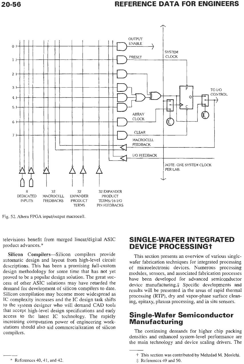
FEEDBACKS PRODUCT TERMS/16
1/0
DEDICATED MACROCELL EXPANDER PRODUCT
TERMS
PIN
FEEDBACKS
Fig.
52. Altera
FPGA
input/output
macrocell
televisions benefit from merged linear/digital
ASIC
product advances.*
Silicon
Compilers-Silicon compilers provide
automatic design and layout from high-level circuit
descriptions. This has been a promising full-custom
design methodology for some time that has not yet
proved
to
be a popular design solution. The great suc-
cess of other
ASIC
solutions may have retarded the
demand for development of silicon compilers to date.
Silicon compilation may become more widespread as
IC
complexity increases and the
IC
design task shifts
to
the system designer who will demand
CAD
tools
that accept high-level design specifications and early
access
to
the latest
IC
technology. The rapidly
increasing computation power
of
engineering work-
stations should also aid commercialization of silicon
compilers.
*
References 40,41,
and
42.
NOTE.
ONE
SYSTEM
CLOCK
PER LAB
SINGLE-WAFER INTEGRATED
DEVICE PROCESSlNGt
This section presents an overview of various single-
wafer fabrication techniques for integrated processing
of microelectronic devices. Numerous processing
modules, sensors, and associated fabrication processes
have been developed for advanced semiconductor
device manufacturing.: Specific developments and
results will be presented in the areas
of
rapid thermal
processing
(RTP),
dry and vapor-phase surface clean-
ing, epitaxy, plasma processing, and
in
situ sensors.
Single-Wafer Semiconductor
Manufacturing
The continuing demands for higher chip packing
densities and enhanced system-level performance are
the main technology and device scaling drivers. The
t
This
section
was
contributed
by
Mehrdad M. Moslehi.
$
References
49
and
50.
INTEGRATED
CIRCUITS
TO
MACROCELL
ARRAY
20-57
0
63
W?
AAP
8
32
32 32 EXPANDER
INPUTS
FEEDBACKS PRODUCT TERMS
/16
I/O
TERMS
PIN
FEEDBACKS
DEDICATED MACROCELL EXPANDER PRODUCT
Fig.
53.
Altera
FPGA
expander
product term array to “fold back”
signals between
macrocells.
SIGNAL ROUTINC
THROUGH
SWITC
BY TRANSISTOR
PASS-GATES
CONTROLLED
B\r
SRAM CELL
LOGIC STATE
LOGIC
BLOCK
Fig.
54.
Xilinx
FPGA
architecture.
(Courtesy
Xilim,
Inc.)
high-performance processor and dense memory chips
now require device integration levels
on
the order of
100-1000 million transistors based on advanced sub-
micron (e.g., 0.13-0.18
pm)
CMOS and
BiCMOS
technologies. This level of integration density places
stringent demands
on
the processing equipment,
device fabrication processes, and manufacturing pro-
cess control. State-of-the-art semiconductor manufac-
turing factories usually employ batch equipment for
high-throughput wafer processing. The high manufac-
turing throughputs (e.g., thousands to over
20,000
wafers/month) and stringent manufacturing process
control requirements are achieved at the cost of
reduced flexibility as well as rapidly escalating cost
of
new generations of advanced processing equipment.
Semiconductor technology scaling also affects wafer
size. Currently, the state-of-the-art chip factories are
set up for 200-mm wafer processing. The wafer size
is
expected to grow
to
300
mm
by
2005.
Single-wafer processing
(SWP)
is an alternative to
batch equipment for various device fabrication pro-
cesses.
As
the wafer size increases beyond 200
mm,
advanced
SWP
equipment will be preferred for many
applications. The factors in favor of
SWP
include com-
patibility with multichamber cluster equipment for
vacuum-integrated processing, improved fabrication
cycle time, and enhanced process repeatability. An
argument against
SWP
has been its inferior processing
throughput compared with the batch equipment.
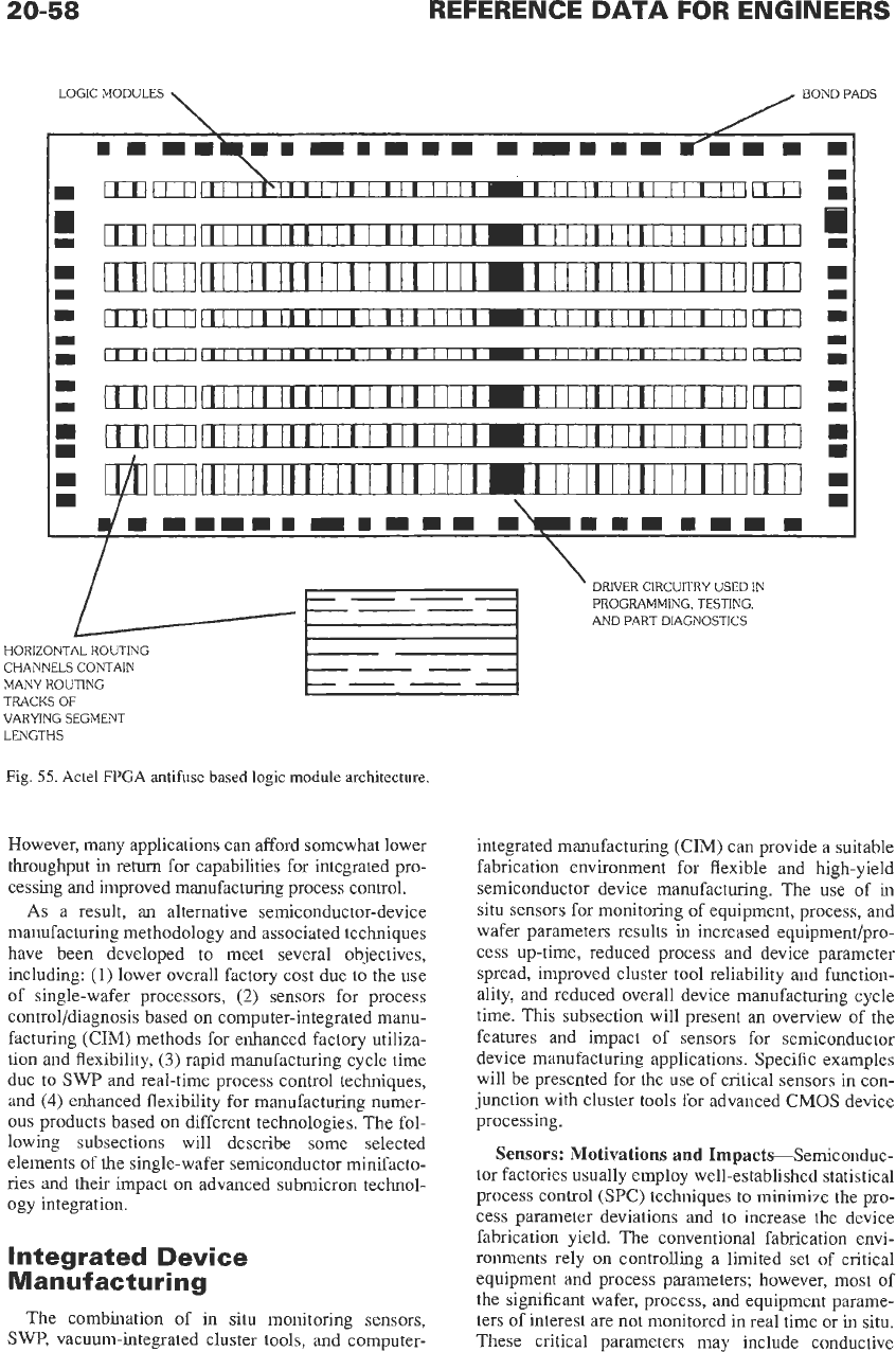
20-58
REFERENCE
DATA
FOR ENGINEERS
\
/
PADS
LOGIC MODULES
[771[1111lllllllllllI1111111=111
IIIIII
IIllll
ClIDI
ml[mrllIIIIIIIIIlIIIlIlI~Ill
IIIIII
IIIlll
m:
'
DRIVER CIRCUITRY USED IN
PROGRAMMING. TESTING.
AND PART DIAGNOSTICS
HORIZONTAL ROUTING
CHANNELS CONTAIN
MANY ROUTING
TRACKS
OF
VARYING SEGMENT
LENGTHS
Fig.
55.
Actel
FPGA
antifuse based logic module architecture.
However, many applications can afford somewhat lower
throughput in return for capabilities for integrated pro-
cessing and improved manufacturing process control.
As
a result, an alternative semiconductor-device
manufacturing methodology and associated techniques
have been developed
to
meet several objectives,
including:
(1)
lower overall factory cost due to the use
of single-wafer processors,
(2)
sensors for process
controVdiagnosis based on computer-integrated manu-
facturing
(CIM)
methods for enhanced factory utiliza-
tion and flexibility,
(3)
rapid manufacturing cycle time
due to
SWP
and real-time process control techniques,
and
(4)
enhanced flexibility for manufacturing numer-
ous
products based on different technologies. The fol-
lowing subsections will describe some selected
elements
of
the single-wafer semiconductor minifacto-
ries and their impact on advanced submicron technol-
ogy integration.
Integrated Device
Manufacturing
The combination of
in
situ monitoring sensors,
SWP,
vacuum-integrated cluster tools, and computer-
integrated manufacturing
(CIM)
can provide a suitable
fabrication environment for flexible and high-yield
semiconductor device manufacturing. The use of in
situ sensors for monitoring of equipment, process, and
wafer parameters results
in
increased equipment/pro-
cess up-time, reduced process and device parameter
spread, improved cluster tool reliability and fimction-
ality, and reduced overall device manufacturing cycle
time. This subsection will present an overview of the
features and impact of sensors for semiconductor
device manufacturing applications. Specific examples
will be presented for the use of critical sensors in con-
junction with cluster tools for advanced
CMOS
device
processing.
Sensors: Motivations and ImpactsSemiconduc-
tor factories usually employ well-established statistical
process control
(SPC)
techniques to minimize the pro-
cess parameter deviations and to increase the device
fabrication yield. The conventional fabrication envi-
ronments rely on controlling a limited set of critical
equipment and process parameters; however, most of
the significant wafer, process, and equipment parame-
ters of interest
are
not monitored in real time or in situ.
These critical parameters may include conductive
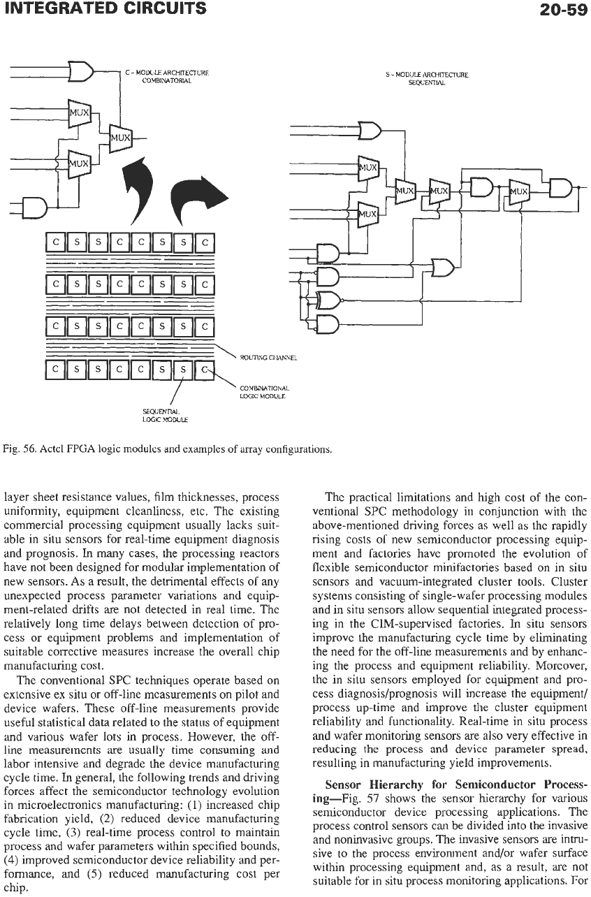
C
-
MODULE ARCHITECTURE
COMBINATORIAL
20-59
S
-
MODULE ARCHITECNRE
SEQUENTN
3
- -
rnjF,y!F.
RoUnNG
CHANNEL
COMBINATIONAL
LOGIC MODULE
SEQUENTIAL
LOGIC
MODULE
Fig.
56.
Actel FFGA logic modules and
examples of
array configurations
layer sheet resistance values, film thicknesses, process
uniformity, equipment cleanliness, etc. The existing
commercial processing equipment usually lacks suit-
able in situ sensors for real-time equipment diagnosis
and prognosis.
In
many cases, the processing reactors
have not been designed for modular implementation of
new sensors.
As
a result, the detrimental effects of any
unexpected process parameter variations and equip-
ment-related drifts are not detected in real time. The
relatively long time delays between detection of pro-
cess or equipment problems and implementation of
suitable corrective measures increase the overall chip
manufacturing cost.
The conventional
SPC
techniques operate based on
extensive ex situ or off-line measurements
on
pilot and
device wafers. These off-line measurements provide
useful statistical data related to the status of equipment
and various wafer lots
in
process. However, the off-
line measurements
are
usually time consuming and
labor intensive and degrade the device manufacturing
cycle time.
In
general, the following trends and driving
forces affect the semiconductor technology evolution
in microelectronics manufacturing:
(1)
increased chip
fabrication yield,
(2)
reduced device manufacturing
cycle time,
(3)
real-time process control
to
maintain
process and wafer parameters within specified bounds,
(4)
improved semiconductor device reliability and per-
formance, and
(5)
reduced manufacturing cost per
chip.
The practical limitations and high cost of the con-
ventional SPC methodology in conjunction with the
above-mentioned driving forces as well as the rapidly
rising costs of new semiconductor processing equip-
ment and factories have promoted the evolution of
flexible semiconductor minifactories based
on
in situ
sensors and vacuum-integrated cluster tools. Cluster
systems consisting of single-wafer processing modules
and in situ sensors allow sequential integrated process-
ing in the CIM-supervised factories.
In
situ sensors
improve the manufacturing cycle time by eliminating
the need for the off-line measurements and by enhanc-
ing the process and equipment reliability. Moreover,
the in situ sensors employed for equipment and pro-
cess diagnosis/prognosis will increase the equipment/
process up-time and improve the cluster equipment
reliability and functionality. Real-time in situ process
and wafer monitoring sensors are also very effective in
reducing the process and device parameter spread,
resulting in manufacturing yield improvements.
Sensor Hierarchy for Semiconductor Process-
ing-Fig.
57
shows the sensor hierarchy for various
semiconductor device processing applications. The
process control sensors can be divided into the invasive
and noninvasive groups. The invasive sensors
are
intru-
sive to the process environment and/or wafer surface
within processing equipment and, as a result,
are
not
suitable for in situ process monitoring applications. For