Middleton W.M. (ed.) Reference Data for Engineers: Radio, Electronics, Computer and Communications
Подождите немного. Документ загружается.

REFERENCE
DATA
FOR ENGINEERS
NONINVASIVE
PROGYOSIS
REAL
TIME
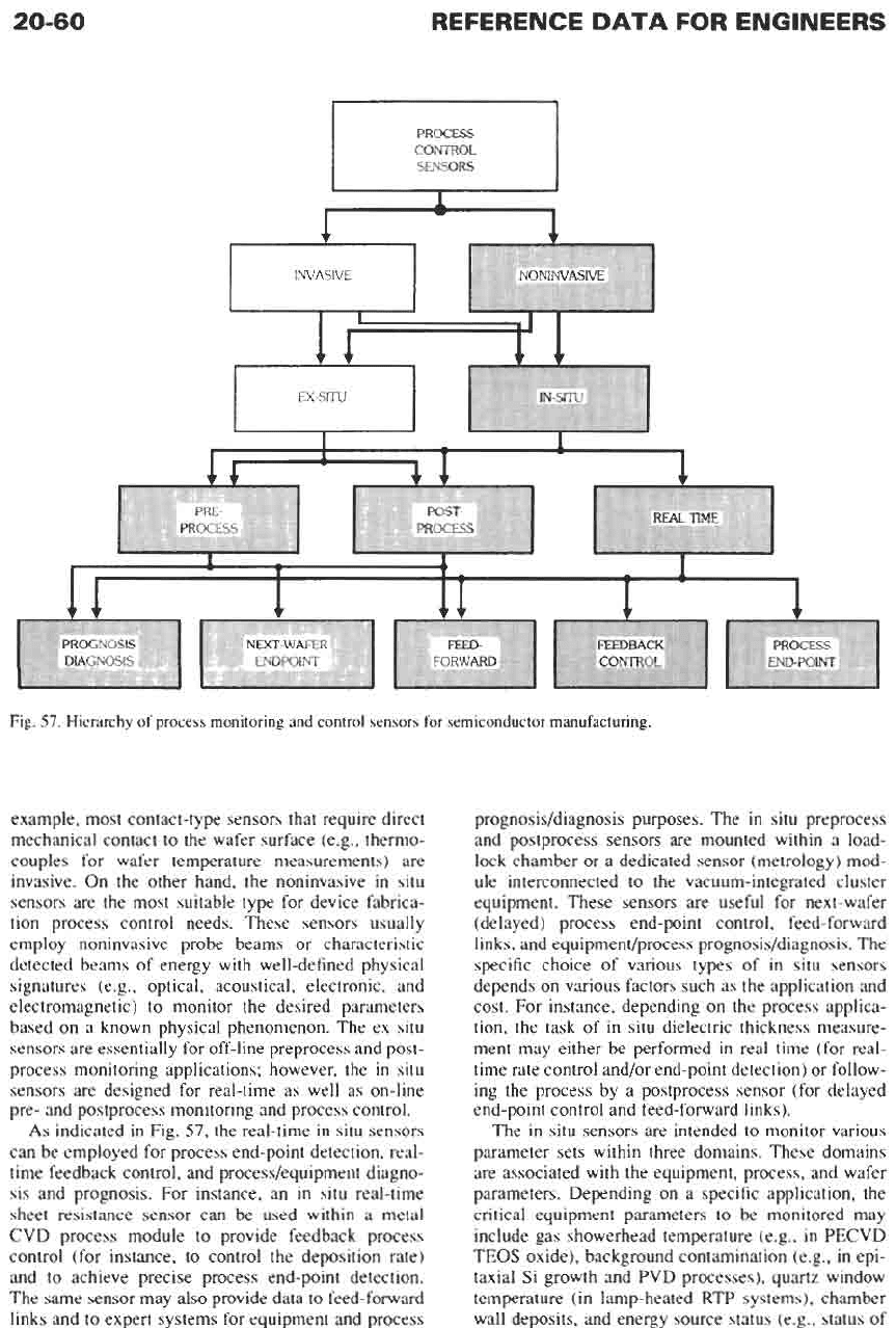
Fig.
57.
Hierarchy of
process
monitoring
and
control sensors for semiconductor manufacturing.
example, most contact-type sensors that require direct
mechanical contact to the wafer surface (e.g., thermo-
couples for wafer temperature measurements)
are
invasive. On the other hand, the noninvasive in situ
sensors
are
the most suitable type for device fabrica-
tion process control needs. These sensors usually
employ noninvasive probe beams or characteristic
detected beams of energy with well-defined physical
signatures (e.g., optical, acoustical, electronic, and
electromagnetic) to monitor the desired parameters
based on a known physical phenomenon. The ex situ
sensors
are
essentially for off-line preprocess and post-
process monitoring applications; however, the in situ
sensors
are
designed for real-time as well as on-line
pre- and postprocess monitoring and process control.
As
indicated in Fig.
57,
the real-time in situ sensors
can be employed for process end-point detection, real-
time feedback control, and process/equipment diagno-
sis and prognosis. For instance, an in situ real-time
sheet resistance sensor can
be
used within a metal
CVD process module to provide feedback process
control (for instance, to control the deposition rate)
and to achieve precise process end-point detection.
The same sensor may
also
provide data to feed-forward
links and to expert systems for equipment and process
prognosis/diagnosis purposes. The in situ preprocess
and postprocess sensors
are
mounted within a load-
lock chamber or a dedicated sensor (metrology)
mod-
ule interconnected to the vacuum-integrated cluster
equipment. These sensors
are
useful for next-wafer
(delayed) process end-point control, feed-forward
links, and equipment/process prognosis/diagnosis. The
specific choice of various types of in situ sensors
depends on various factors such as the application and
cost. For instance, depending on the process applica-
tion, the task of in situ dielectric thickness measure-
ment may either
be
performed
in
real time (for real-
time rate control and/or end-point detection) or follow-
ing the process by a postprocess sensor (for delayed
end-point control and feed-forward links).
The in situ sensors
are
intended to monitor various
parameter sets within three domains. These domains
are associated with the equipment, process, and wafer
parameters. Depending on a specific application, the
critical equipment parameters to be monitored may
include gas showerhead temperature (e.g., in PECVD
TEOS
oxide), background contamination (e.g.,
in
epi-
taxial Si
growth
and PVD processes), quartz window
temperature (in lamp-heated
RTP
systems), chamber
wall deposits, and energy source status (e.g., status of
INTEGRATED CIRCUITS
DIRECT FEEDBACK CONTROLLER
20-6
1
4
lamps and the total lamp power in RTP). Additional
equipment parameters are the gas flow rate and pres-
sure settings in a processing reactor. However, the pro-
cess parameters are directly governed by the
equipment parameters (both controlled and uncon-
trolled parameters). Depending
on
a specific applica-
tion, the process parameters of interest to monitor may
be wafer temperature, process gas flow field, plasma
density, and plasma electron energy.
In
general, a
semiconductor wafer exposed to a process contains the
most important parameters that have
to
be controlled.
This is due to the fact that the wafer parameters have a
direct impact
on
device performance and yield.
For
example, in a CVD or PVD (sputter deposition) pro-
cess used for deposition of dielectric or conductive
films, the important wafer-level parameters include
film thickness, refractive index, stress, conductive-
layer sheet resistance, and thickness uniformity.
Among the above-mentioned three parameter
domains, the equipment parameters
are
the easiest to
monitor. The equipment parameters can be directly
adjusted and controlled, whereas the process and wafer
parameters
are
dependent variables. Monitoring and
control of the desired process and wafer parameters
require specialized noninvasive in situ sensors and
advanced control techniques. Proper adjustments of
process and wafer parameters
are
usually performed
by varying the equipment parameters. The process
parameters are functions of the equipment variables
via equipment models, and the wafer parameters are
determined by the process parameters via process
models.
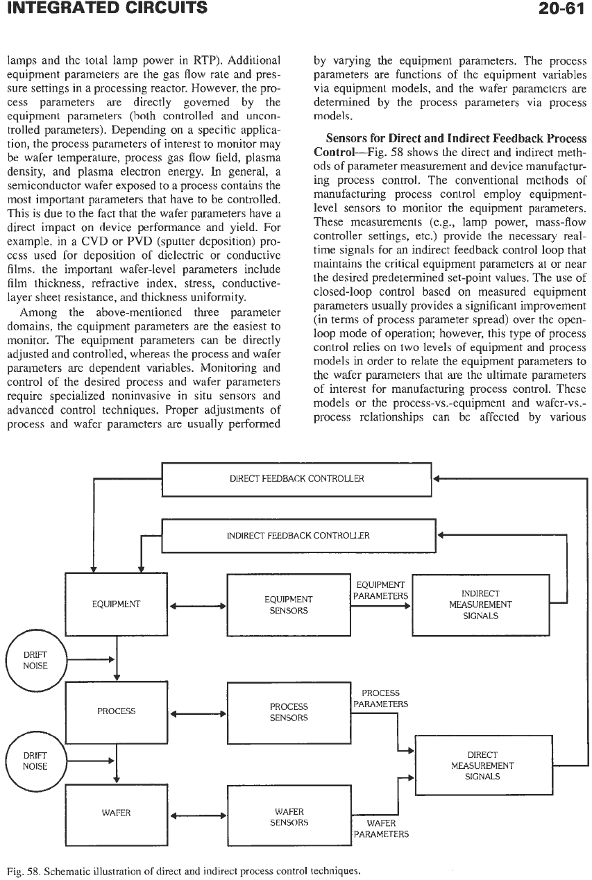
Sensors for Direct and Indirect Feedback Process
Control-Fig.
58
shows the direct and indirect meth-
ods of parameter measurement and device manufactur-
ing process control. The conventional methods of
manufacturing process control employ equipment-
level sensors to monitor the equipment parameters.
These measurements (e.g., lamp power, mass-flow
controller settings, etc.) provide the necessary real-
time signals for an indirect feedback control loop that
maintains the critical equipment parameters at or near
the desired predetermined set-point values. The use of
closed-loop control based
on
measured equipment
parameters usually provides a significant improvement
(in terms of process parameter spread) over the open-
loop mode of operation; however, this type of process
control relies
on
two levels of equipment and process
models in order to relate the equipment parameters to
the wafer parameters that are the ultimate parameters
of interest for manufacturing process control. These
models or the process-vs.-equipment and wafer-vs.-
process relationships can be affected by various
.
INDIRECT FEEDBACK CONTROLLER
~
EQUIPMENT
EQUIPMENT
PARAMETERS
MEASUREMENT
EQUIPMENT
NOISE
PROCESS
PROCESS PARAMETERS
SENSORS
DIRECT
MEASUREMENT
SIGNALS
NOISE
SENSORS
PARAMETERS
Fig.
58.
Schematic illustration
of
direct and indirect process control techniques.
20-62
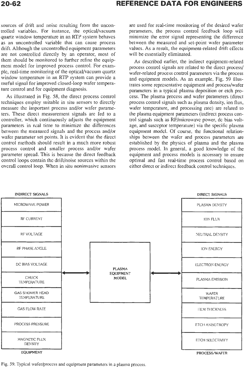
RF PHASE ANGLE
DC
BIAS
VOLTAGE
PLASMA
EQUIPMENT
MODEL
TEMPERATURE
GAS SHOWER
HEAD
TEMPERATURE
sources of drift and noise resulting from the uncon-
trolled variables. For instance, the optical/vacuum
quartz window temperature in an RTP system behaves
as an uncontrolled variable that can cause process
drift. Although the uncontrolled equipment parameters
are not controlled directly by an operator, most of
them should be monitored to further refine the equip-
ment model for improved process control. For exam-
ple, real-time monitoring of the optical/vacuum quartz
window temperature in an RTP system can provide a
useful signal for improved closed-loop wafer tempera-
ture control and for equipment diagnosis.
As illustrated in Fig.
58,
the direct process control
techniques employ suitable in situ sensors to directly
measure the important process and/or wafer parame-
ters. These direct measurement signals are fed to a
controller, which continuously adjusts the equipment
parameters in real time
to
minimize the differences
between the measured signals and the process and/or
wafer parameter set points. It is evident that the direct
control methods should result in a much more robust
process contxol and smaller process and/or wafer
parameter spread. This is because the direct feedback
control loops contain the drift/noise sources within the
overall control loop. When in situ noninvasive sensors
-
INDIRECT SIGNALS
MICROWAVE POWER
RF CURRENT
are used for real-time monitoring of the desired wafer
parameters, the process control feedback loop will
minimize the error signal representing the difference
between the measured and set-point wafer parameter
values. As a result, the equipment-related drift effects
will be essentially eliminated.
As described earlier, the indirect equipment-related
process control signals
are
related to the direct process/
wafer-related process control parameters via the process
and equipment models.
As
an example, Fig.
59
illus-
trates some representative equipment and process/wafer
parameters
in
a typical plasma deposition or etch pro-
cess. The plasma process and wafer parameters (direct
process control signals such as plasma density, ion flux,
wafer temperature, and processing rate) are related to
the plasma equipment parameters (indirect process con-
trol signals such
as
RF/microwave power, dc bias volt-
age, and susceptor temperature) via the specific plasma
equipment model. Of course, the functional relation-
ships between the wafer and process parameters are
established by the physics of plasma and
the
plasma
process model.
In
general, a good knowledge of
the
equipment and process models is necessary to ensure
optimal and fast real-time process control based on
either direct or indirect feedback control techniques.
DIRECT SIGNALS
I
I
PLASMA
DENSITY
Fig.
59.
Typical wafer/process and
equipment
parameters
in
a plasma process
20-63
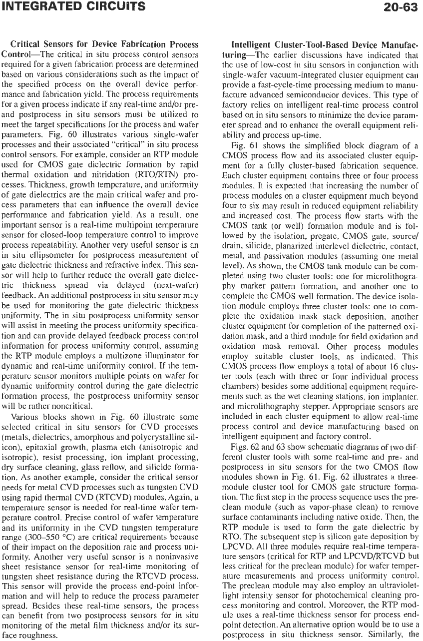
Critical Sensors for Device Fabrication Process
Control-The critical in situ process control sensors
required for a given fabrication process
are
determined
based on various considerations such as the impact of
the specified process on the overall device perfor-
mance and fabrication yield. The process requirements
for a given process indicate if any real-time and/or pre-
and postprocess in situ sensors must be utilized to
meet the target specifications for the process and wafer
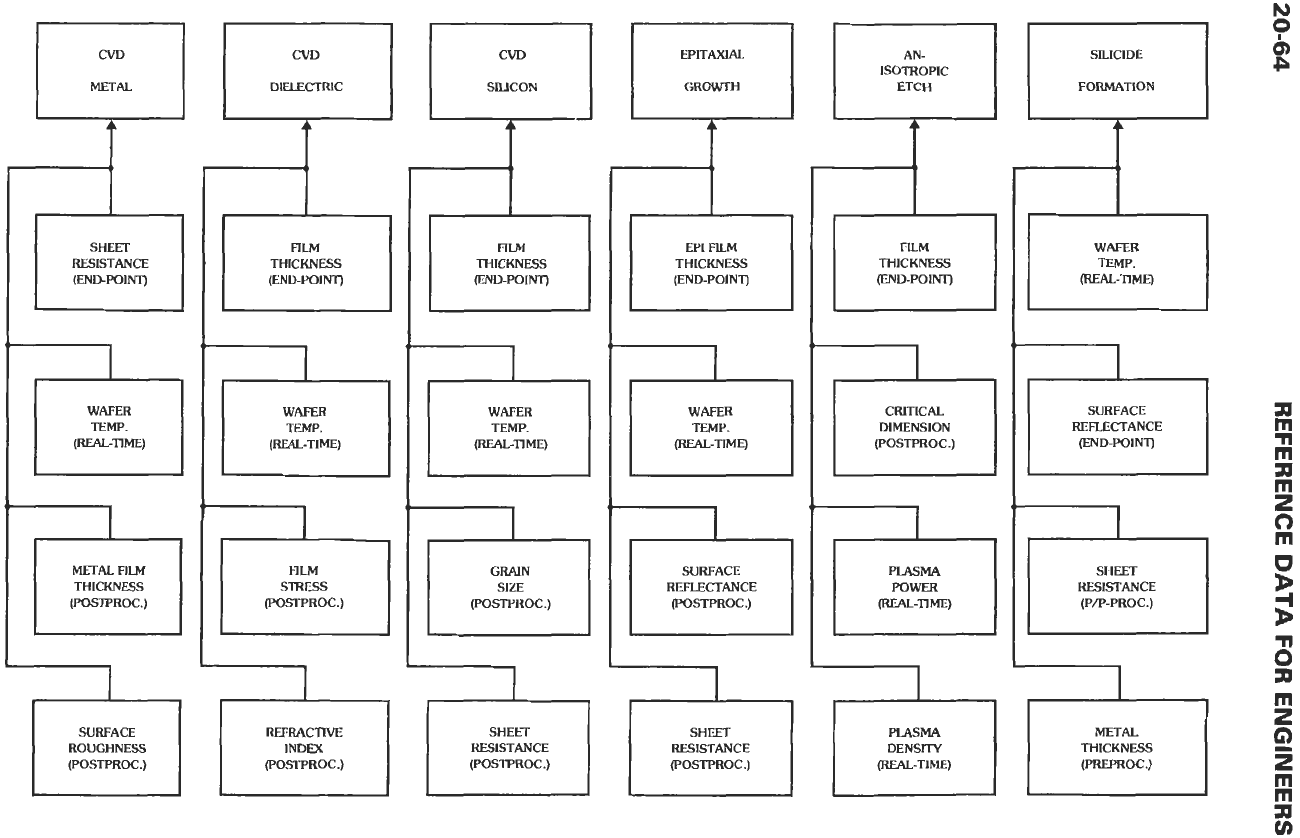
parameters. Fig. 60 illustrates various single-wafer
processes and their associated “critical” in situ process
control sensors. For example, consider an RTP module
used for CMOS gate dielectric formation by rapid
thermal oxidation and nitridation (RTO/RTN) pro-
cesses. Thickness, growth temperature, and uniformity
of gate dielectrics are the main critical wafer and pro-
cess parameters that can influence the overall device
performance and fabrication yield. As a result, one
important sensor is a real-time multipoint temperature
sensor for closed-loop temperature control to improve
process repeatability. Another very useful sensor is an
in situ ellipsometer for postprocess measurement of
gate dielectric thickness and refractive index. This sen-
sor will help to further reduce the overall gate dielec-
tric thickness spread via delayed (next-wafer)
feedback. An additional postprocess in situ sensor may
be used for monitoring the gate dielectric thickness
uniformity. The in situ postprocess uniformity sensor
will assist in meeting the process uniformity specifica-
tion and can provide delayed feedback process control
information for process uniformity control, assuming
the RTP module employs a multizone illuminator for
dynamic and real-time uniformity control. If the tem-
perature sensor monitors multiple points on wafer for
dynamic uniformity control during the gate dielectric
formation process, the postprocess uniformity sensor
will be rather noncritical.
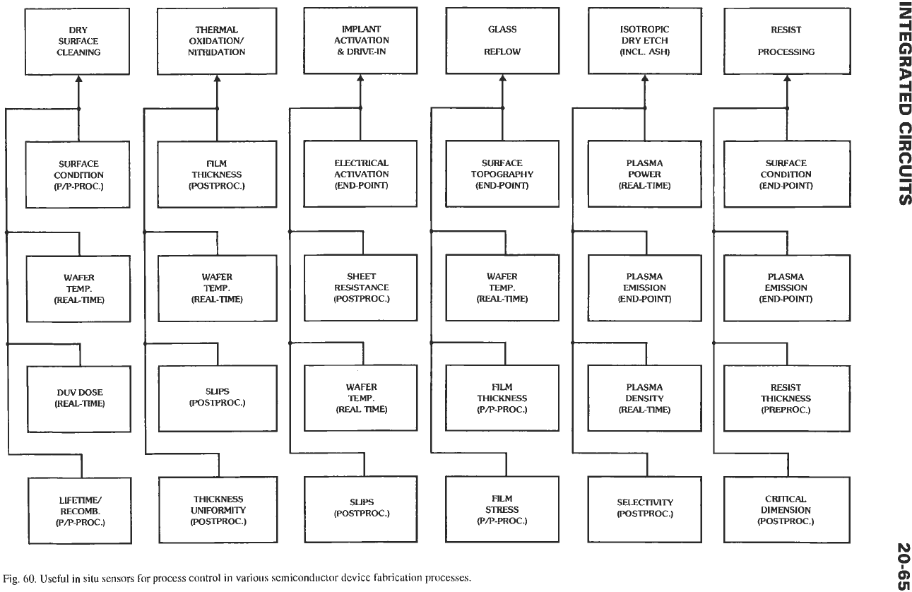
Various blocks shown in Fig. 60 illustrate some
selected critical in situ sensors for CVD processes
(metals, dielectrics, amorphous and polycrystalline sil-
icon), epitaxial growth, plasma etch (anisotropic and
isotropic
j,
resist processing, ion implant processing,
dry surface cleaning, glass reflow, and silicide forma-
tion. As another example, consider the critical sensor
needs for metal CVD processes such as tungsten CVD
using rapid thermal CVD (RTCVD) modules. Again, a
temperature sensor is needed for real-time wafer tem-
perature control. Precise control of wafer temperature
and its uniformity in the CVD tungsten temperature
range (300-550
“C)
are critical requirements because
of their impact on the deposition rate and process uni-
formity. Another very useful sensor is a noninvasive
sheet resistance sensor for real-time monitoring of
tungsten sheet resistance during the RTCVD process.
This sensor will provide the process end-point infor-
mation and will help to reduce the process parameter
spread. Besides these real-time sensors, the process
can benefit from two postprocess sensors for
in
situ
monitoring of the metal film thickness and/or its sur-
face roughness.
Intelligent Cluster-Tool-Based Device Manufac-
turing-The earlier discussions have indicated that
the use of low-cost in situ sensors in conjunction with
single-wafer vacuum-integrated cluster equipment can
provide a fast-cycle-time processing medium to manu-
facture advanced semiconductor devices. This type of
factory relies on intelligent real-time process control
based on in situ sensors to minimize the device param-
eter spread and to enhance the overall equipment reli-
ability and process up-time.
Fig. 61 shows the simplified block diagram
of
a
CMOS process flow and its associated cluster equip-
ment for a fully cluster-based fabrication sequence.
Each cluster equipment contains three or four process
modules.
It
is expected that increasing the number of
process modules on a cluster equipment much beyond
four to six may result in reduced equipment reliability
and increased cost. The process flow starts with the
CMOS tank (or well) formation module and is fol-
lowed by the isolation, pregate, CMOS gate, source/
drain, silicide, planarized interlevel dielectric, contact,
metal, and passivation modules (assuming one metal
level). As shown, the CMOS tank module can be com-
pleted using two cluster tools: one for microlithogra-
phy marker pattern formation, and another one to
complete the CMOS well formation. The device isola-
tion module employs three cluster tools: one to com-
plete the oxidation mask stack deposition, another
cluster equipment for completion of the patterned oxi-
dation mask, and a third module for field oxidation and
oxidation mask removal. Other process modules
employ suitable cluster tools, as indicated. This
CMOS process flow employs a total of about
16
clus-
ter tools (each with three or four individual process
chambers) besides some additional equipment require-
ments such as the wet cleaning stations, ion implanter,
and microlithography stepper. Appropriate sensors are
included in each cluster equipment to allow real-time
process control and device manufacturing based on
intelligent equipment and factory control.
Figs. 62 and 63 show schematic diagrams of two dif-
ferent cluster tools with some real-time and pre- and
postprocess in situ sensors for the two CMOS flow
modules shown
in
Fig.
61.
Fig. 62 illustrates a three-
module cluster tool for CMOS gate structure forma-
tion. The first step in the process sequence uses the pre-
clean module (such as vapor-phase clean)
to
remove
surface contaminants including native oxide. Then, the
RTP module is used to form the gate dielectric by
RTO. The subsequent step
is
silicon gate deposition
by
LPCVD. All three modules require real-time tempera-
ture sensors (critical for RTP and LPCVDBTCVD but
less critical for the preclean module) for wafer temper-
ature measurements and process uniformity control.
The preclean module may also employ an ultraviolet-
light intensity sensor for photochemical cleaning pro-
cess monitoring and control. Moreover, the RTP mod-
ule uses a real-time thickness sensor for process end-
point detection. An alternative option would be to use a
postprocess in situ thickness sensor. Similarly, the
'r
SHEET
RESISTANCE
(END-POINT)
TEMP.
(REAL-TIME)
METAL
FILM
THICKNESS
(POSTPROC.)
SURFACE
ROUGHNESS
(POSTPROC.)
u
I
THICKNESS
(ENDPOINT)
1
(REAL-TIME) (REAL-TIME)
REFRACTIVE
RESISTANCE
EPITAXIAL
GROWTH
THICKNESS
pk-l
(REAL-TIME)
REFLECTANCE
lS0TROPIC
Lfi
DIMENSION
1
7
RESISTANCE
FORMATION
(REAL-TlME)
SURFACE
REFLECTANCE
(END-POINT)
RESISTANCE
THICKNESS
SURFACE OXIDATION/
NITRIDATION
t
r+
(POSTPROC.)
+
(POSTPROC.)
SUPS
(POSTPROC.)
ACTIVATION
&
DRIVEAN
ELECTRICAL
ACIlVATION
(ENDPOINT)
RESISTANCE
(POSTF'ROC.)
1
SURFACE
TOPOGRAPHY
(ENDPOINT)
THICKNESS
Y
(P/P-PROC.)
(POSTPROC.)
RECOMB. UNIFORMITY
(PP-PROC.) (POSTPROC.) (P/P-PROC.)
Fig.
60.
Useful
in
situ
sensors
for process control
in
various semiconductor device fabrication processes.
PLASMA
EMISSION
(END-POINT)
PLASMA
DENSITY
(POSTPROC.)
El
PROCESSING
Y
SURFACE
CONDITION
(END-POINT')
EMISSION
(END-POINT)
RESIST
THICKNESS
(F'REPROC.)
CRITICAL
DIMENSION
(POSTPROC.)
20-66
FLOWMODULES
r-€
_-
PHFWTF
GATE
SILICIDE
MLO
FOR
RE
B
COSTACT
MI.TA1.
1
PASSIVATION
I
I
I
I
I
I
I
I
I
I
I
I
I
I
I
I
I
I
I
I
I
I
I
I
I
I
I
I
I
I
I
I
I
I
I
I
I
I
I
I
I
I
I
I
I
I
I
I
I
I
I
I
I
I
I
I
I
I
I
LPCVD silicon process module also
uses
a silicon
thickness sensor for process end-point detection. The
load-lock
(or
metrology) chamber contains a slip sen-
sor
for postprocess monitoring of possible RTO-
induced slip dislocations. A sheet resistance sensor
may
be
used for postprocess monitoring of LPCVD in
situ-doped silicon sheet resistance. Another load-lock
sensor can
be
used to monitor the effectiveness of the
surface preclean process.
Fig.
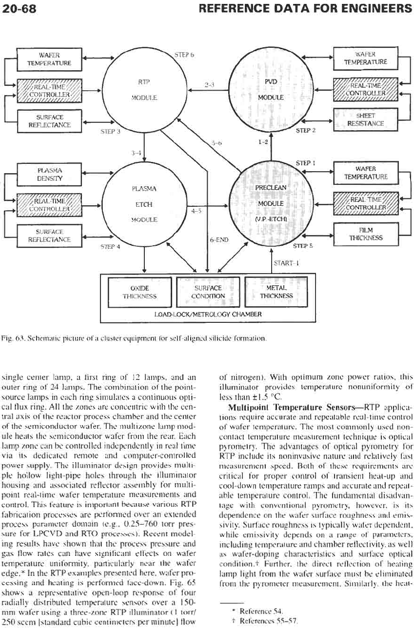
63
illustrates the example of a four-module
cluster tool for self-aligned silicide formation. The
process sequence employs preclean for native oxide
removal, refractory metal sputtering,
RTP
silicide for-
mation, plasma etch for removal of unreacted refrac-
tory metal and metal nitride, vapor-phase clean, and
finally another
RTP
cycle for silicide annealing. All the
critical real-time and pre- and postprocess sensors
are
also shown.
RTP for Integrated Device
Processing
Conventional and state-of-the-art semiconductor
factories employ batch furnaces for many thermal fab-
rication steps.
Various
applications include gate and
field oxidations, low-pressure chemical-vapor deposi-
tion
(LPCVD)
(e.g., for polysilicon and silicon
nitride), and thermal anneals (e.g., for junction forma-
tion and glass reflow). A significant number of other
fabrication processes, however,
are
already based
on
SWP.
Examples include plasma etch and deposition,
ion implantation, and microlithography. The current
trend toward replacement of batch processes with
SWP
is evident from the increasing market share for
cluster tool equipment with
SWP
modules.
RTP
is an
obvious choice to replace batch furnaces for thermal
processing in a semiconductor minifactory environ-
ment. Advanced RTP tools
are
based on modular
designs compatible with vacuum-integrated cluster
equipment. High-performance multizone illuminators
with cylindrical symmetry have been applied to vari-
ous
processes including RTO, CVD
of
tungsten and
amorphous/polycrystalline
silicon, silicide formation,
sinter, epitaxy, as well as high-temperature rapid ther-
mal annealing (RTA).* Concurrent use of multizone
illuminators and multipoint temperature sensors pro-
vides a capability for real-time wafer temperature con-
trol and process uniformity optimization.? Moreover,
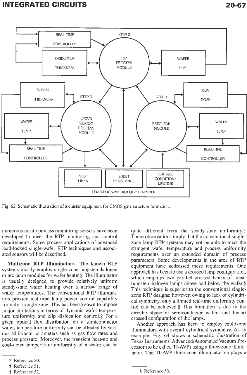
INTEGRATED CIRCUITS
20-67
I
LOAD-LOCK/METROLOGY CHAMBER
Fig.
62.
Schematic illustration
of a
cluster equipment for
CMOS
gate structure formation.
numerous in situ process monitoring sensors have been
developed to meet the RTP monitoring and control
requirements. Some process applications of advanced
load-locked single-wafer RTP techniques and associ-
ated sensors will be described.
Multizone
RTP
Illuminators-The known RTP
systems mostly employ single-zone tungsten-halogen
or arc lamp modules for wafer heating. The illuminator
is usually designed to provide relatively uniform
steady-state wafer heating over a narrow range of
wafer temperatures. The conventional RTP illumina-
tors provide real-time lamp power control capability
for only a single zone. This has been known to impose
major limitations in terms of dynamic wafer tempera-
ture uniformity and slip dislocation control.$ For a
given optical flux distribution on a semiconductor
wafer, temperature uniformity can be affected by vari-
ous
additional parameters such as gas flow rates and
process pressure. Moreover, the transient heat-up and
cool-down temperature uniformity of a wafer can be
*
Reference
50.
t
Reference
5
1.
j
Reference
52.
quite different
from
the steady-state uniformity.$
These observations imply that the conventional single-
zone lamp RTP systems may not be able to meet the
stringent wafer temperature and process uniformity
requirements over an extended domain of process
parameters. Some developments in the area of RTP
equipment have addressed these requirements. One
approach has been to use a crossed lamp configuration,
which employs two parallel crossed banks of linear
tungsten-halogen lamps above and below the wafer.$
This technique is superior to the conventional single-
zone RTP designs; however, owing to lack of cylindri-
cal symmetry, only a limited real-time uniformity con-
trol can be achieved.$ This limitation is due to the
circular shape
of
semiconductor wafers and linear/
crossed configuration of
the
lamps.
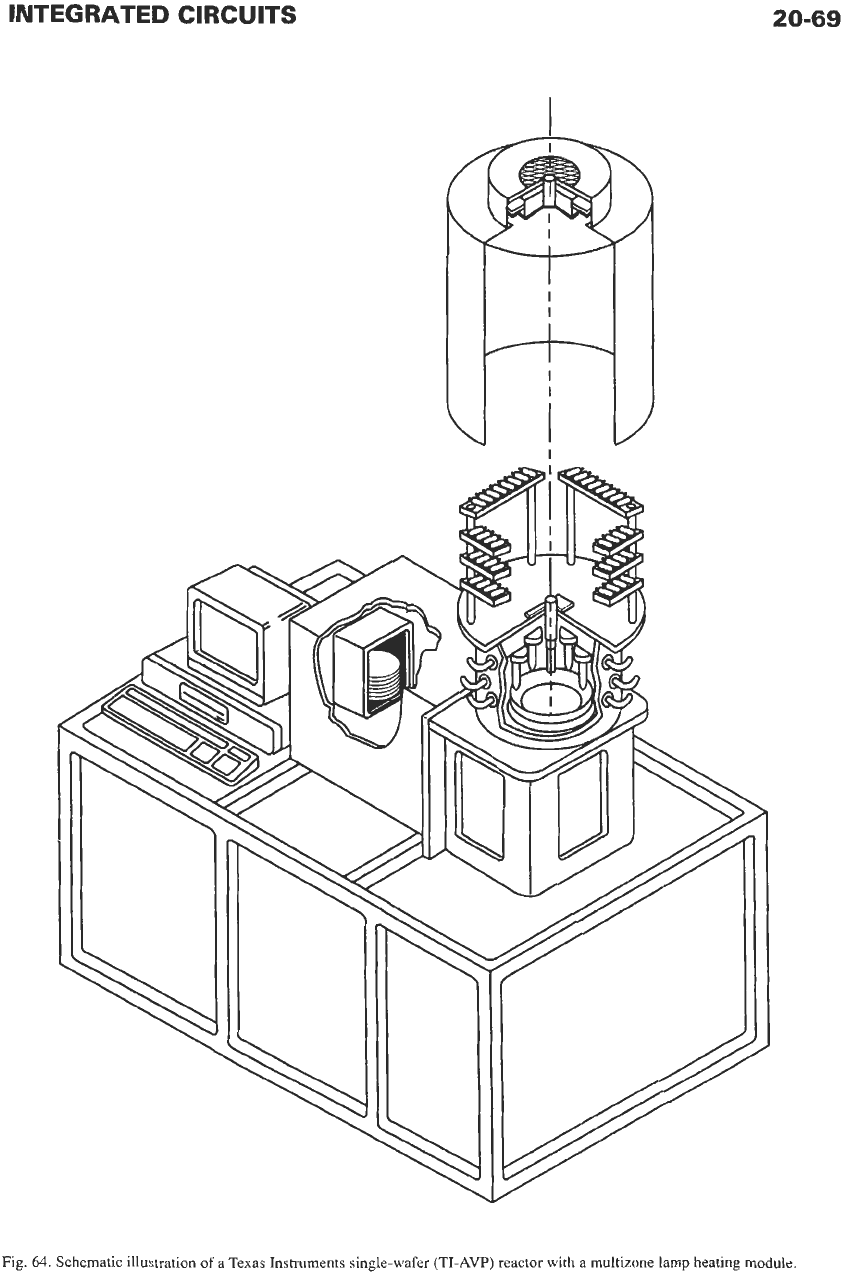
Another approach has been to employ multizone
illuminators with overall cylindrical symmetry. As an
example, Fig.
64
shows a schematic illustration
of
Texas Instruments' Advanced/Automated Vacuum Pro-
cessor (to be called TI-AVP) using a three-zone illumi-
nator. The TI-AVP three-zone illuminator employs a
8
Reference
53.
20-68
REFERENCE
DATA
FOR
ENGINEERS
RTP
MODULE
OXIDE
THICKNESS
SURFACE
CONDITION
PVD
MODULE
MODULE
METAL
THICKNESS
I
LOADLOCK/METROLCGY CHAMBER
I
Fig.
63.
Schematic picture of a cluster equipment for self-aligned silicide formation.
single center lamp, a first ring of 12 lamps, and an
outer ring of
24
lamps. The combination of
the
point-
source lamps in each ring simulates a continuous opti-
cal flux ring. All the zones
are
concentric with the cen-
tral axis of the reactor process chamber and the center
of the semiconductor wafer. The multizone lamp mod-
ule heats the semiconductor wafer from the rear. Each
lamp zone can
be
controlled independently in real time
via its dedicated remote and computer-controlled
power supply. The illuminator design provides multi-
ple hollow light-pipe holes through the illuminator
housing and associated reflector assembly for multi-
point real-time wafer temperature measurements and
control. This feature is important because various RTP
fabrication processes are performed over an extended
process parameter domain (e.g., 0.25-760 torr pres-
sure for
LPCVD
and
RTO
processes). Recent model-
ing results have shown that the process pressure and
gas flow rates can have significant effects on wafer
temperature uniformity, particularly near the wafer
edge.* In the
RTP
examples presented here, wafer pro-
cessing and heating is performed face-down. Fig.
65
shows a representative open-loop response of four
radially distributed temperature sensors over a
150-
mm wafer using a three-zone RTP illuminator
(1
torr/
250
sccm [standard cubic centimeters per minute] flow
of
nitrogen).
With
optimum zone power ratios, this
illuminator provides temperature nonuniformity of
less than
f1.5
"C.
Multipoint Temperature Sensor-RTP applica-
tions require accurate and repeatable real-time control
of wafer temperature. The most commonly used non-
contact temperature measurement technique is optical
pyrometry.
The
advantages of optical pyrometry for
RTP include its noninvasive nature and relatively fast
measurement speed. Both of these requirements are
critical for proper control of transient heat-up and
cool-down temperature ramps and accurate and repeat-
able temperature control. The fundamental disadvan-
tage with conventional pyrometry, however,
is
its
dependence on
the
wafer surface roughness and emis-
sivity. Surface roughness is typically wafer dependent,
while emissivity depends on a range of parameters,
including temperature and chamber reflectivity, as well
as
wafer-doping characteristics and surface optical
condition.? Further, the direct reflection of heating
lamp light from
the
wafer surface must be eliminated
from the pyrometer measurement. Similarly, the heat-
*
Reference 54.
t
References 55-57.
INTEGRATED CIRCUITS
20-69
Fig.
64.
Schematic illustration
of
a Texas Instruments
single-wafer
(TI-AW) reactor
with
a
multizone lamp heating
module