Mitin V.V., Sementsov D.I., Vagidov N.Z. Quantum mechanics for nanostructures
Подождите немного. Документ загружается.


8.2 Characterization with nanoscale resolution 273
where D is the probability of electron transmission through the air gap. In
accordance with Eq. (3.156), this probability is defined as
D ≈ exp
−
2L
h
-
2m
e
U
eff
, (8.8)
where U
eff
is the magnitude of the effective potential barrier between the tip and
the surface of the sample. For the majority of “tip–object” pairs the mean value of
the potential barrier is equal to U
eff
≈ 4–5 eV. To estimate the tunneling current,
let us assume that the electron beam which emanates from the outermost atom of
the tip has a diameter of about d = 0.4 nm to provide high scanning resolution.
On substituting the values of the parameters L = 0.5 nm and U
eff
= 4eVinto
Eq. (8.8) we get D ≈ 10
−5
. Thus, taking into account that n ≈ 10
28
m
−3
,we
get n
0
≈ 10
23
m
−3
. By substituting the obtained value of n
0
and v ≈ 10
6
m
s
−1
into Eq. (8.6) we can estimate the magnitude of the tunneling current as
I
T
≈ 2 × 10
−9
A.
The magnitude of the tunneling current, I
T
, depends exponentially on the
distance, L, between the tip and the sample. Therefore, on increasing the distance
only by 0.1 nm the magnitude of D and, correspondingly, the tunneling current I
T
decrease by a factor of almost 10. Thus, small changes in the height of the surface
relief induce substantial changes in the tunneling current, which provides the high
resolution capabilities of the STM. Owing to this extremely high sensitivity, an
STM may provide images of surfaces with a resolution of 0.01 nm in the vertical
direction and with an accuracy of atomic size in the horizontal plane.
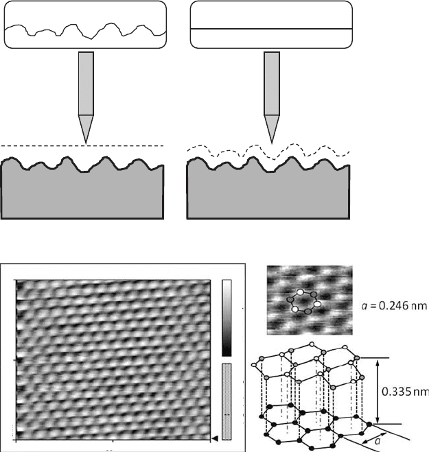
Usually two operation modes are used, for studying surfaces of different
materials. The operating regime of constant height requires the motion of the tip
in a strictly horizontal plane over the surface. The magnitude of the tunneling
current will depend on the distance between the tip and the scanned surface.
By registering the tunneling current, I
T
, at each point of the surface and using
computer processing, we can plot the image of the surface relief. In the operating
regime of constant current a feedback system is used to maintain a constant
tunneling current by changing the distance between the tip and the surface at
each point of the scanned surface (see Fig. 8.9). The visualization of the surface
relief is done using the data of the vertical displacements of the scanning device.
As an example, a scanned surface of graphite is shown in Fig. 8.10.
Each of these two regimes has its advantages and drawbacks. The regime of
constant height is fast enough because the system does not need to move the
scanning device up and down. The drawback of this regime is that information
may be obtained only from very flat and smooth surfaces. In the regime of constant
current irregular surfaces may be scanned with high accuracy. The drawback of
this regime is that the measurements take too much time. Let us note that the
quality of the tip and the radius of its end define the resolution capabilities of the
274 Nanostructures and their applications
Sample
Tip
trajectory
Tunneling current
Sample
Tip
trajectory
Tunneling current
(a) (b)
Figure 8.9 Tip motion
over the scanned surface
in the two operating
regimes of an STM: (a)
constant-height mode and
(b) constant-current
mode.
Topography - Scan forward
4.16 nm
Y*
0 nm
0 nm
x*
4.16 nm
Topography range
Line fit 192 pm
Figure 8.10 A picture of a graphite surface obtained by an undergraduate student
carrying out an experiment from the lab course at the Undergraduate Nanoelectronics
Laboratory at the University at Buffalo. There are two different positions of carbon
atoms in a crystal lattice of graphite: one with a neighboring atom in the plane below
(gray balls) and one without a neighbor in the plane below (white balls). It is clearly
seen that the upper layer of graphite is not flat: the atoms that have neighboring
atoms in the lower plane are more strongly attracted to each other than are the atoms
depicted as white balls. Therefore, the atoms depicted as white balls are slightly above
the plane while the atoms depicted as gray balls are slightly below the plane.
STM and the quality of the image. The end of the tips used in industry has the
size of several atoms.
In the working regime of an STM the distance between the tip and the surface
is about L ≈ 0.3−1 nm, therefore the probability of air molecules being between
them is very low at standard atmospheric pressure. Therefore, we may assume
that passage of the tunneling current takes place under almost vacuum conditions.
8.2 Characterization with nanoscale resolution 275
Sample
Laser
Cantilever
Tip
Photodetector
Figure 8.11 A schematic
representation of the
atomic-force microscope.
We can draw an important conclusion from the above for the practical operation
of an STM: the operational regime of the STM in most cases does not require high
vacuum, which is a necessary requirement, for example, for electron microscopes
of other types.
The main drawback of an STM is the following: the object studied has to be
a conductor, i.e., it must be either a metal or a doped semiconductor, otherwise
the tunneling current would not flow. Therefore, we cannot study the surface
structures of dielectrics, for example the surface structure of diamond, with the
help of STM techniques.
8.2.3 Atomic-force microscopy
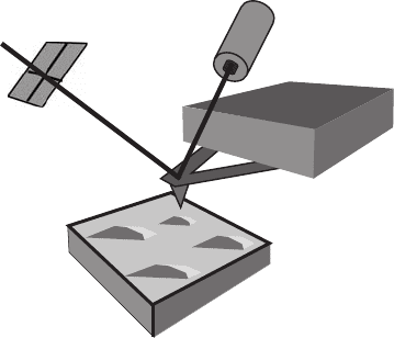
Five years after the invention of the STM in 1986, the atomic-force microscope
(AFM) was developed. The measured parameter in an AFM is the interatomic
interaction force between the tip and the surface of the sample. The operational
principles of the AFM are the following. At the distance at which a tunneling
current between the tip and the conducting surface occurs, there appears an
appreciably large force between the tip and surface. This force, as in the case
of tunneling current, significantly depends on the gap between the tip and the
surface of the object studied. The force can be detected from the elastic deflection
of the so-called cantilever which has the scanning tip at its end (see Fig. 8.11).
A photodetector provides the detection of small deflections of the cantilever’s
end.
An AFM allows us to study the surface of any object regardless of its con-
ductivity. However, new problems occur in this case: the dependence of the
interaction force between the tip and the sample surface is complex and this
force does not depend on the sample–tip distance in a monotonic way.
At large distances between the tip and the surface there is an attractive force,
which at smaller distances becomes a repulsive force. The distance between the
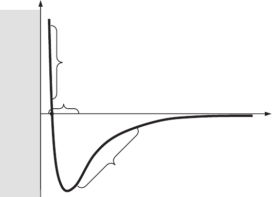
276 Nanostructures and their applications
F
r
Sample surface
0
repulsive force
attractive force
contact mode
non-contact mode
tapping mode
Figure 8.12 The
dependence of the
interatomic force, F ,on
the distance between the
tip and the surface, r ,
showing the intervals of
the three operational
regimes: (1) contact
mode, (2) tapping mode,
and (3) non-contact mode.
cantilever’s tip and the scanned surface at which the type of the force changes
is approximately equal to 1 nm. Therefore, the distance range within which
measurements can be made is very limited. Thus, it is very important to calibrate
the measurement device carefully, otherwise the image obtained will be difficult
to interpret.
Figure 8.12 shows schematically the dependence of the interaction force
between the tip and the scanned surface on the distance between them. It also
shows the types of operational regimes corresponding to different distances.
This new type of microscope allows us to overcome the principal limitation
of the scanning-tunneling microscope: the AFM allows us to obtain images
of conducting as well as non-conducting surfaces with atomic resolution under
atmosphere conditions (see Fig. 8.13). An additional advantage of the AFM is the
possibility of visualizing, together with the surface relief, its electric, magnetic,
elastic, and other properties. Omitting the details, the operational principles of the
AFM can be described as follows. The largest input into the interaction between
the tip and the sample surface is from the force between an atom at the end of the
tip and the nearest atoms of the sample surface. The closer the tip to the scanned
surface, the more strongly atoms of the tip are attracted to the nearest atoms of
the sample surface. The force of attraction will increase as these atoms approach
each other, until the electron clouds of these atoms begin to repel each other.
With a further decrease of the interatomic distance the electrostatic repulsion
exponentially weakens the attraction force. At a distance between the atoms of
the tip and the surface of about 1 nm the forces of attraction and repulsion become
equal to each other.
Depending on the type of interaction, the AFM may operate in one of the
following regimes (see Fig. 8.12). In the contact mode the tip comes very close
8.2 Characterization with nanoscale resolution 277
BA
BA
Periodic arrangement
of ridges
Period
Microrib
Ridge
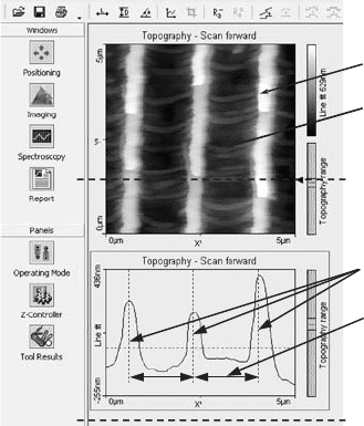
Figure 8.13 The structure
of the scale of a Morpho
butterfly wing obtained by
an undergraduate student
carrying out an
experiment from the lab
course at the
Undergraduate
Nanoelectronics
Laboratory at the
University at Buffalo. You
can clearly see ridges and
microribs that connect
ridges. The lower picture
shows a cross-section of
the butterfly-wing scale
along the horizontal line
AB.
to the surface of the sample and the deflection of the cantilever is caused by the
mutual repulsion of atoms on the end of the tip and on the sample surface. It is
caused by the overlap of electron clouds and Coulomb repulsion of the atomic
nuclei. In the non-contact mode, which corresponds to the region of attraction
forces, the AFM registers the attractive van der Waals force acting between the
scanning tip and the sample surface. The gap between the end of the tip and
the surface in the non-contact mode is usually about 5–10 nm. The intermediate
regime between contact and non-contact modes is the mode of periodic instant
physical contacts of the tip with the surface during the scanning process. This
mode is called the tapping mode. In this regime the cantilever with the tip
oscillates with some fundamental resonance frequency having an amplitude of
about 50–100 nm. The fundamental frequency of the cantilever with the tip
is determined when the cantilever is far away from the surface. In operational
mode the tip is moved closer to the surface and, at amplitudes of about 50–
100 nm, the tip comes into brief physical contact with the sample surface when
the cantilever has its maximum deflection down from the equilibrium position.
This substantially changes the frequency, phase, and amplitude of the cantilever
oscillations. All three of these parameters can be measured. The tapping mode is
characterized by higher resolution in the horizontal plane than is possible in the
contact-mode regime.
On comparing the operational principles of scanning-tunneling and atomic-
force microscopes, we can see that they have much in common. The main dif-
ference between them is the design of the probe. In an STM the probe (the tip)
must be rigidly clamped and must not touch the surface, and the sharper the tip
the better. In an AFM the tip is mounted on the deflecting cantilever and can
be operated in regimes in which the oscillating tip touches the surface of the
278 Nanostructures and their applications
material being studied for a short time during each period of oscillation (the tip
literally “taps” the sample surface). Therefore, the tip must be strong enough,
which requires a larger thickness of the end of the tip in contrast to the case of
an STM tip. Moreover, a tip with a very sharp end will provide a smaller signal,
which will be difficult to detect.
The first cantilevers for AFMs were made of gold foil with a diamond tip
or of aluminum foil with a tungsten wire. Later developers switched to silicon
cantilevers, which are widely used currently. The deflections and oscillations of
the cantilever may be detected by a laser beam that is reflected from a mirror
sputtered onto the top of the cantilever (see Fig. 8.11).
From the discussion above, it is clear that the most important component
both of a scanning-tunneling and of an atomic-force microscope is the tip. The
standard technology for sharpening the tip is etching. For sharpening of the tip
also ion sharpening is used: the tip is bombarded by a beam of ions, which
removes excessive material from the tip’s end. As practice shows, a tip has a
finite lifetime. During operation the distance between the tip and the sample
is very small. Accidental contact with the scanned surface can damage the tip.
Therefore, this component requires constant attention. When the properties of
the tip deteriorate, the tip is usually replaced or it is sharpened without moving
it away from the microscope.
8.2.4 Scanning-probe nanotechnology
The modification of scanning-probe microscopes allows us not only to charac-
terize nanostructures, but also to fabricate nanostructures on the atomic level.
When the voltage between the sample and the tip is slightly greater than that in
the operational tunneling regime, the atom from the sample surface (precisely,
the ion) can be transferred to the tip. By changing the polarity of the applied
voltage we can force the ion to return to the sample surface. If during these two
events the tip has been moved, then the ion will be placed onto a new position
on the surface. So, it is possible to manipulate the positions of individual atoms
with the help of a tip. For this kind of technique we need (a) a high-quality
STM, which operates at low temperatures, in order for the atoms not to disperse
as a result of thermal motion, (b) a proper tip, and (c) certain skills. Such a
possibility of manipulation of atoms by use of an STM was demonstrated for
the first time by the members of one of the IBM research centers. In 1985 they
were granted a patent on the possibility of moving individual atoms from the
end of the STM’s tip onto the sample’s surface. Moreover, in 1989 they were
able to construct the logo of their company “IBM” on the surface of a gold film
using 35 atoms of xenon. This event is considered the birth of scanning-probe
nanotechnology.
Nowadays, there exist several methods for the displacement and assembly
of nanostructures from individual atoms and molecules. The first method, as
8.2 Characterization with nanoscale resolution 279
described above, consists of the capturing and displacing of atoms by applying a
higher voltage. The sample must be at ultra-high vacuum during this procedure,
otherwise the surface would quickly be covered by atoms from the environment.
By filling the gap between the sample and the tip with inert gases we can obtain the
same results as would be obtained in vacuum. So, the method of scanning-probe
nanolithography in liquid and gaseous media was developed. By introducing into
the gap between the tip and the sample’s surface specifically selected substances
and by changing the applied voltage, we can initiate chemical reactions at the
point of the tip’s contact with the surface. An example of such technology is the
method of local anode oxidization of thin metallic films. This method allows one
to obtain on the surface of a metal a pattern formed by its oxides with a width of
several tens of nanometers. This method is used to fabricate electronic circuits
of ultra-small size.
An AFM can also be used for the modification of a surface. The simplest
method is to scratch the surface. With the help of direct contact of the end of
the tip with the sample’s surface, we can make pits and grooves or flatten the
surface. For this purpose tips made from hard materials such as diamond are used.
The capabilities of an AFM to modify a surface can be enhanced if the tip is made
conductive. Being able to induce an electric current between the sample and the
tip allows the operator to heat locally the surface, control the chemical reactions
that can take place in the contact region, and transfer atoms and molecules from
the tip to the sample and vice versa. The possibilities of modification of surfaces
with the help of the AFM are similar to the possibilities that the STM has. At the
same time, AFM techniques allow one to obtain images of fabricated structures
even if their surfaces are not conducting.
Thus, the most important achievement of scanning-probe microscopy is that
it is not only an instrument for the characterization of nanostructures but also an
instrument for the fabrication of nanostructures.
The main problem of scanning-probe nanotechnology is its low production
output. A single probe, even at maximum speed of operation, cannot provide mass
production. This drawback can be overcome by the development of multiprobe
devices. In such devices the nanostructures are produced simultaneously by
several tens or even thousands of probes.
Currently STMs and AFMs are scientific instruments that are used widely.
An entirely new industry that manufactures various components of micro-
scopes, including tips and cantilevers, as well as complex research systems, has
emerged.
Example 8.2. Estimate the pressure of an electron beam and the mechanical
strain caused by the ponderomotive forces on the region of surface under the tip
of the STM. The values of operational characteristics are the following: current
I = 10
−2
A, applied voltage U = 5 V, radius of the tip r = 20 nm, and gap
between tip and surface L = 1nm.

280 Nanostructures and their applications
Reasoning. The current density in the electron beam can be defined as
j =
I
S
= nev, (8.9)
where n is the electron concentration in the beam, e the electron charge, and v
the electron’s velocity. The pressure of electrons in the beam is defined as
P =
F
S
=
p
S t
=
(nvS t)m
e
v
S t
= nm
e
v
2
, (8.10)
where S is the cross-sectional area of the electron beam, nvS t is the number of
electrons with mass m
e
reaching the surface during the time period t at a given
current I , and m
e
v is the momentum of an individual electron. The velocity of
electrons in the beam can be estimated as
v =
2eU
m
e
≈ 1.3 × 10
6
ms
−1
. (8.11)
Taking into account the derived relationships, we obtain for the pressure of the
electron beam, P, the following expression:
P =
I
Sev
m
e
v
2
=
m
e
I
eS
2eU
m
e
=
I
πr
2
2m
e
U
e
≈ 6 × 10
7
Pa. (8.12)
The surface region under the tip experiences the action of the ponderomotive
forces which are induced by the electric field created between the tip and the
surface. Mechanical strain can be defined as negative pressure acting on the
surface, i.e., in this case the surface particles are attracted to the tip. Considering
the tip and the surface as two plates of a plane capacitor, we can estimate the
magnitude of the force acting between these two plates:
F
E
= QE
2
= Sσ E
2
= Sσ
E
2
= S
0
E
2
2
, (8.13)
where Q is the charge of one of the plates, E
2
is the field induced by the other
plate, σ is the surface charge density, E = σ/(
0
) is the electric field of the
charged capacitor, and is the dielectric permittivity of the medium between the
tip and the surface. As a result, the negative pressure on the studied region of
the surface is equal to
P
E
=
F
E
S
=
0
E
2
2
=
0
U
2
2L
2
≈ 10
8
Pa. (8.14)
Thus, by controlling the applied voltage and the gap between the tip and the
surface, we can achieve sufficiently large values of the positive and negative
pressure, which will allow us to pull electrons away from the surface and to
deform locally the sample surface.
8.2 Characterization with nanoscale resolution 281
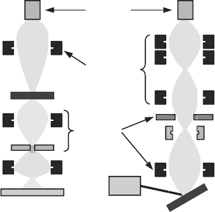
Source
Objective
System
Scanning Electron
Microscope
Condenser
Scan Coils
SampleDetector
Transmission Electron
Microscope
Sample
Screen
Projector Lens
(a) (b)
Figure 8.14 The TEM (a)
and SEM (b).
8.2.5 Electron microscopy
The electron microscope, which uses an electron beam instead of a light beam
for imaging, was developed in 1935. The invention of the electron microscope
became possible because of the rapid development of quantum mechanics at the
beginning of the twentieth century, when it was discovered that the electron has
the properties of a wave as well as those of a particle. As we have already learned,
the waves associated with electrons exhibit interference and diffraction, which
are inherent to light waves. At the same time, electrons are charged particles
and their motion can be controlled by electric and magnetic fields. Electron
beams can be deflected by electric and magnetic fields just as light rays can
be deflected by optical lenses. The focussing systems of electron beams are
called electron lenses. The role of a light source in an optical microscope in
electron microscopes is taken by the electron gun (usually a heated tungsten wire
that serves as the source of electrons). The emitted electrons pass through the
electron-condensing lens, which regulates the intensity of the flux and the area
of the scanned surface subjected to exposure. After passing through the electron
lens, which is used as an objective lens, the electron beam is directed onto a
luminescent screen, which transforms the electron-distribution image into an
image that can be either photographed or directly observed. There are two major
types of electron microscopes: the transmission-electron microscope (TEM) and
the scanning-electron microscope (SEM).
The TEM (see Fig. 8.14(a)) measures the intensity of the electron beam
transmitted through the sample and it has the following principal features. Since
the electron beam is strongly absorbed and/or scattered by atoms, the sample
is placed in an evacuated chamber. For the same reasons the sample must be
very thin (about 100 nm) and sample preparation is a rather difficult problem.
282 Nanostructures and their applications
The SEM (see Fig. 8.14(b)) does not have restrictions on the thickness of the
sample. The SEM design has much in common with the design of the TEM. The
principal difference is that the electron beam is focussed onto a certain spot of
the surface and the reflected or secondary electrons are studied. The process of
interaction of the incident electron beam with the material of the object being
studied results in the following products: (a) a beam of reflected electrons, (b)
a beam of secondary and Auger electrons, and (c) radiation in the visible and
X-ray range. These are registered by corresponding detectors, transformed into
electric signals, amplified, and displayed. With the help of the deflection system,
the incident electron beam is moved over the sample and in this way scans its
surface. As a result, a magnified image of the studied region of the surface is
formed on the display. The possibility of simultaneous registration of different
types of radiation allows one to obtain comprehensive information about the
structure being studied. The resolution of a TEM can be as low as 2
˚
A, which
allows one to obtain images of individual atoms and molecules. The resolution
of an SEM comes close to the resolution of a TEM and currently it reaches 5
˚
A.
However, the SEM has a couple of advantages over the TEM. Since in an SEM
the electrons which participate in the formation of an image do not penetrate the
sample, there is no restriction on the thickness of the sample. The procedure of
sample preparation is significantly simplified and there is no need for ultra-high
vacuum as for the TEM, which simplifies the design of an SEM and reduces its
cost.
There are also new devices that have been developed and are being developed.
They use the principles described above for the measurement of electrical, optical,
mechanical, and other properties of the sample surface. Currently the methods
described above are widely used not only for the study of surface relief, but
also for the control of the technological processes relating to the fabrication
of nanostructures and nanomaterials. For example, the following system of two
microscopes has been developed. Within an SEM system on its sample stage, an
STM is mounted. First, with the help of the STM, a desired spot on the sample
surface is identified. After this, the chosen spot is carefully studied by the SEM,
which has much higher resolution (subatomic resolution) than that of the STM.
Combinations of SEM and AFM techniques are also being developed.
8.3 Selected examples of nanodevices and systems
The tendency towards miniaturization in electronics is not only sustained but has
intensified. Researchers have fabricated new types of electronic devices of ultra-
small size, which have become the basis of nanoelectronics. Nanostructures are
in turn used for the development of new devices, whose operational principles
are fundamentally different from those of existing conventional semiconductor
devices such as diodes and transistors.