Mitin V.V., Sementsov D.I., Vagidov N.Z. Quantum mechanics for nanostructures
Подождите немного. Документ загружается.


C.5 The energy spectrum of an electron in a crystal 403
and the atomic state with the set of quantum numbers {q}:
ψ
q
(r) =
n
C
n
ψ
0q
(r − a
n
). (C.76)
Here, a
n
is the translation vector of the crystalline lattice, and the coefficients C
n
define
the probability amplitudes of finding an electron at a corresponding atom. Let us note that
the electron wavefunction in a periodic inner-crystal potential has, according to Bloch’s
theorem, in the general case the form
ψ
q
(r) = G
k
(r)e
ik·r
, (C.77)
where k is the electron wavevector and the function G
k
(r) is a periodic function. The
translation by a lattice vector a
n
leads to multiplication of the electron wavefunction in
the crystal by the exponential factor corresponding to this shift:
ψ
q
(r +a
n
) = e
ik·a
n
ψ
q
(r). (C.78)
From this expression it follows that the expansion coefficients, C
n
,inEq.(C.76) must
have the following form:
C
n
= e
ik·a
n
. (C.79)
The form of the Bloch electron wavefunction in a crystal (Eq. (C.77)) indicates the
commonality with free-electron character of its behavior. The factor G
k
(r) modulates the
wavefunction of a free electron e
ik·r
with the periodicity of the crystalline lattice potential.
Taking into account the temporal dependence, the electron wavefunction in a crystal can
be presented in the following form:
ψ
q
(r, t) = G
k
(r)e
i(k·r−E
q
t/h
-
)
. (C.80)
C.5.2 Energy bands in crystals
The one-electron wavefunction (C.76) is a solution of the Schr
¨
odinger equation with a
self-consistent inner-crystal potential, U
eff
(r), i.e.,
ˆ
Hψ
q
(r) = E
q
ψ
q
(r), (C.81)
ˆ
H =−
h
-
2
2m
e
∇
2
+U
eff
(r). (C.82)
The eigenvalue of the electron energy for the non-normalized wavefunction ψ
q
(r)is
defined by the general expression
E
q
=
ψ
∗
q
ˆ
Hψ
q
dV
ψ
∗
q
ψ
q
dV
, (C.83)

404 Appendix C. Crystals as atomic lattices
where dV = dx × dy × dz. By calculating the integrals in Eq. (C.83) and taking into
account orthonormalization of atomic wavefunctions, we obtain
E
q
= E
0q
−
W
q
−
n
A
qn
e
ik · a
n
. (C.84)
Here E
0q
is the corresponding atomic level, and the average value of the perturbation of
an atomic potential calculated using the unperturbed state is defined as
W
q
=
ψ
∗
0q
(r)[U
eff
(r) − U
0
(r)]ψ
0q
(r)dV, (C.85)
where U
0
(r) is the atomic potential. The summation in Eq. (C.84) is done as a rule over
the nearest-neighboring atoms which surround the atom which is chosen as the origin.
This is because the exchange integral, A
qn
, responsible for the splitting of the level E
0q
for a neighboring atom significantly exceeds the exchange integrals for non-neighboring
atoms.
Calculation of Eq. (C.84) for a simple cubic lattice gives the following expression for
the energy dispersion in the band formed from atomic level E
0q
:
E
q
= E
0q
−
W
q
− 2 A
q
[cos(ak
x
) +cos(ak
y
) +cos(ak
z
)]. (C.86)
When the crystal is formed from individual atoms, the electron energy it had in an isolated
atom, E
0q
, is decreased by
W
q
, and is spread out into an energy band as a result of
interaction with neighboring atoms. At the limits of the band the electron energy changes
periodically with the components of the wavevector k. The same decrease and spreading
into a band happen to each stationary energy level of an isolated atom. The width of each
allowed energy band is proportional to the exchange integral, E
q
= 4 A
q
, and is mostly
defined by the overlap of wavefunctions of neighboring atoms. For valence electrons this
overlap is significant and thus the width of the allowed energy band can reach several
electron-volts. For electrons of inner shells the splitting is small. Thus, for K-electrons
in a crystal of metallic sodium, Na, the splitting is just 2 ×10
−19
eV! Therefore, the
corresponding band has the form of a narrow energy level.
Let us discuss the dispersion relation for electrons in crystals using expression (C.86)
for a cubic lattice. It has very much in common with the equation for elastic waves in
a discrete chain of atoms. First of all, let us note that the substitution of wavevector
projection
k
α
→ k
α
+
2π
a
n
α
,α= x, y, z, (C.87)
where n
α
is an integer number, changes neither the dispersion relation nor the wavefunc-
tion. Therefore, instead of considering all possible values of the wavevector, it suffices to
limit our consideration to the interval
−
π
a
≤ k
α
≤
π
a
, (C.88)
C.5 The energy spectrum of an electron in a crystal 405
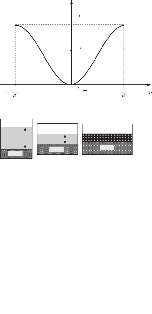
k
E
0q
+ 2A
q
E 2A
q
E
0
0q
q
aa
E
Figure C.10 The first
Brillouin zone. Here
E
0q
= E
0q
−
W
q
.
(a)
Empty
Filled
E
g
E
g
(b) (c)
Empty
Filled
Filled
Empty
Overlap
Figure C.11 Energy bands
in the cases of (a) a
dielectric (E
g
> 5eV),
(b) a semiconductor
(E
g
< 5eV),and(c)a
metal (E
g
= 0eV).
which for electron waves in crystals is called the first Brillouin zone (see Fig. C.10). Thus,
the electron wavevector, k, in a crystal is not defined unambiguously and therefore it is
called the quasiwavevector. This vector is related to the quasimomentum by
p = h
-
k. (C.89)
The allowed energy values for stationary states, E
q
(k), are limited to a band delimited
by
E
0q
−
W
q
− 2 A
q
≤ E
q
≤ E
0q
−
W
q
+ 2A
q
. (C.90)
The energy intervals, E
g
, that lie between the allowed energy bands are forbidden for
electrons in stationary states (see Fig. C.11). These forbidden energy bands are called
bandgaps.
Using periodic boundary conditions, we can show that inside of allowed bands the
projections of the wavevector k
α
have discrete values
k
α
=
2π
L
α
n
α
,α= x, y, z, (C.91)
where integer numbers n
α
independently take on the values ±1, ±2,...,±N
α
/2, and
thesizeofthesampleisL
α
= N
α
a. Since the number of atoms in the sample is

406 Appendix C. Crystals as atomic lattices
enormous, i.e.,
N =
L
x
L
y
L
z
a
3
= nV, (C.92)
where n ≈ 10
28
m
−3
, for a macroscopic sample the distance between the adjacent levels
even in the widest band is not greater than 10
−15
eV. For this reason the discreteness of
the parameter k
α
and the energy E
q
(k) in the allowed bands can be neglected.
C.5.3 Filling energy bands
As shown previously, each allowed band with the set of quantum numbers {q}corresponds
to N stationary states, which can, according to the Pauli principle, contain no more than
2N electrons with opposite spins. Therefore, the way of filling bands significantly depends
on the valency of the atoms forming the crystal. Let us first consider a crystal of univalent
lithium, Li, whose atoms have the electron configuration 1s
2
2s
1
. N sublevels of the lowest
allowed band, which is formed from atomic levels with quantum numbers n = 1and
l = 0, are completely filled by 1s-electrons. N atoms have 2N such electrons. The next
allowed band is formed from atomic levels with quantum numbers n = 2andl = 0. Since
there is only one 2s-electron, N electrons can fill only N/2 sublevels, i.e., this band is
only half-filled. The picture for the filling of the two highest energy bands (completely or
partly filled) of univalent metals is similar.
If the valency of an element is equal to two (or is even), then the last band must be
completely filled. However, if the adjacent bands overlap, which is widely encountered
in real crystals, then incompletely filled bands can have elements with arbitrary valency.
Thus, for beryllium, Be, with electron configuration 1s
2
2s
2
, the energy bands which
correspond to atomic levels with n = 2andl = 0 and with n = 2andl = 1overlap,
forming one wide band. Therefore, beryllium, Be, is a metal.
The difference in the form of filling of the highest allowed band is the basis for crystals’
classification according to their conducting properties. The highest of the completely filled
bands is usually called the valence band. The maximum energy in this band is denoted
as E
v
and is called the top of the valence band. The lowest partially filled or completely
unfilled band is called the conduction band. The minimum energy in this band is denoted
as E
c
andiscalledthebottom of the conduction band. Metals are crystals whose valence
band is filled completely and whose conduction band is not completely filled. Dielectrics
are crystals whose valence band is completely filled and whose conduction band is empty.
The region separating the valence and conduction bands, called the bandgap,has,for
good dielectrics a width, E
g
, of several electron-volts (see Fig. C.11).
C.5.4 Effective mass
The solutions of the Schr
¨
odinger equation (C.81) describe the behavior of electrons in
a crystal in the absence of external fields. However, the response of an electron sys-
tem to applied external fields is of practical interest. For analysis of electron behavior
in a crystal in an external field an approximation called the effective mass method is
widely used. The effective mass itself can be introduced using the dispersion relation.
C.5 The energy spectrum of an electron in a crystal 407
Let us expand the energy E
q
(k) in a series near one of the extremum points k
0
in the first
Brillouin zone:
E
q
(k) = E
q
(k
0
) +
1
2
α
∂
2
E
q
∂k
2
α
k
α
=k
0α
(
k
α
− k
0α
)
2
. (C.93)
To describe the motion of an electron in a periodic field of a crystal in the same way as
we describe the motion of a free electron, let us introduce the tensor of inverse effective
mass, the components of which on the main axes have the form
1
m
∗
q
α
=
1
h
-
2
∂
2
E
q
∂k
2
α
k
α
=k
0α
. (C.94)
Then, the electron dispersion relation in a crystal (Eq. (C.93)) takes the same form as that
of a freely moving particle whose inertial properties are different along each of the axes:
E
q
(k) = E
q
(k
0
) +
α
h
-
2
(k
α
− k
0α
)
2
2m
∗
qα
. (C.95)
If all three components of the tensor 1/m
∗
q
α
are the same in crystals with a cubic lattice, we
can use the scalar effective mass m
∗
q
. In this case the dispersion relation can be presented
in the form
E
q
(k) = E
q
(k
0
) +
h
-
2
(k − k
0
)
2
2m
∗
q
. (C.96)
Near the bottom of the band, where the function E
q
(k) has its minimum, the effective
mass of the electron m
∗
q
is positive, since at the point of the minimum
∂
2
E
q
∂k
2
α
k=k
0
> 0. (C.97)
Near the top of the band the function E
q
(k) has its maximum, and the second derivative
(C.97)isnegativeandm
∗
q
< 0. The effective mass, just like an ordinary mass, relates a
force applied to the particle to the acceleration produced. If m
∗
q
< 0 then the direction
of electron acceleration is opposite to the direction of the applied force. This must not
be a surprise, since the effective mass of the electron takes into account the influence of
the periodic crystalline potential on the electron. The influence of a periodic field and an
external force on the electron, which has wave properties, can lead to such an effect.
Let us write the one-electron Schr
¨
odinger equation for an electron in a crystal in the
presence of external forces:
−
h
-
2
2m
e
∇
2
ψ
q
(r) + [E
q
−U
eff
(r) + U (r)]ψ
q
(r) = 0. (C.98)
Here, the inner-crystal potential U
eff
(r) is a periodic function, which is usually unknown.
The function U (r) describes a non-periodic field, which affects the electron through the
408 Appendix C. Crystals as atomic lattices
defects of crystalline structure and external electric and magnetic fields. Equation (C.98)
in the approximation of the effective mass for a cubic lattice can be reduced to the
following equation:
−
h
-
2
2m
∗
q
∇
2
ϕ
q
(r) +[E
q
−U (r)]ϕ
q
(r) = 0, (C.99)
where the unknown function U
eff
(r) is absent and, instead of the mass of a free electron,
m
e
, we introduce the electron effective mass, m
∗
q
. The new wavefunction ϕ
q
(r) is related
to Bloch’s modulation factor, G
q
(r) which is a property of the electron wavefunction,
(C.77)by,
ψ
q
(r) = G
q
(r)ϕ
q
(r). (C.100)
Equation (C.99) has the simplest form in the absence of external fields in an ideal (i.e.,
without defects) crystalline structure:
−
h
-
2
2m
∗
q
∇
2
ϕ
q
(r) = E
q
ϕ
q
(r). (C.101)
Equation (C.101) describes the motion of an electron in a crystal as the motion of a free
particle with mass equal to the effective mass, m
∗
q
, and energy, E
q
, which defines a sta-
tionary energy state of an electron in one of the allowed bands. The electron wavefunction
in this case has the form of a de Broglie wave:
ϕ
q
(r, t) = Ae
i(k·r−E
q
(k)t/h
-
)
, (C.102)
where the dependence of the electron energy, E
q
, on the wavevector, k,isdefinedby
Eq. (C.86). Knowledge of the form of the dispersion relation, E
q
(k), and the wave-
function, ϕ
q
(k, t ), allows us to find the most important characteristics related to the
behavior of the electron subsystem in general.
C.5.5 Quasiparticles – electrons and holes
In the expression for the wavefunction (C.102) the energy E
q
(k) is the total electron
energy in the energy band defined by the set of quantum numbers {q}. It contains the
electron kinetic energy and energy of interaction with all other electrons and nuclei. Let
us expand the expression (C.86) in series over the wavenumbers near the extremum point
k
0
= 0:
E
q
(k) = E
0q
−
W
q
− 6 A
q
+ A
q
a
2
k
2
= E
−
q
+
p
2
2m
∗
q
, (C.103)
wherewehaveintroducedp = h
-
k and
E
−
q
= E
0q
−
W
q
− 6 A
q
, (C.104)
m
∗
q
=
h
-
2
2A
q
a
2
=
2h
-
2
E
q
a
2
, (C.105)
C.5 The energy spectrum of an electron in a crystal 409
where E
q
is the width of the allowed band. From the equations obtained above it follows
that the magnitude of the electron effective mass, m
∗
q
, is inversely proportional to the
width of the band, E
q
. For the inner bands the magnitudes of A
q
and E
q
are small
and therefore the electron effective mass there is large. The consequence of this is larger
inertia of electrons of inner bands and their weak response to external influences. Only in
the conduction band is the magnitude A
q
such that the effective mass of an electron, m
∗
q
,
is similar to the mass of a free electron, m
e
. Thus, in the approximation considered here,
we can present the total electron energy in a crystal in the form of the kinetic energy of
some pseudo-electron with mass m
∗
q
:
E
qn
= E
q
(k) − E
−
q
=
p
2
2m
∗
q
. (C.106)
The electron in a crystal is called a pseudo-particle because its “momentum” is a
quasimomentum, i.e., it is a periodic quantity in momentum space and all its physically
different quantum states can be reduced to the first Brillouin zone:
−
h
-
π
a
≤ p
α
≤
h
-
π
a
. (C.107)
Moreover, the mass of such an “electron” has not much in common with the mass of a
free electron and, as we have already noted, the effective mass of an electron at the top of a
band may even be negative. Therefore, we named it a “pseudo-electron,” which reflects the
unusual properties of this particle. Thus, with the help of the formal method considered
here, we can reduce the complex problem of the motion of electrons interacting with each
other and with nuclei to the problem of the motion of free pseudo-electrons.
Let us now discuss the question of how to present the dispersion relation near the
maximum of the E
q
(k) dependence, i.e., near the top of a band near the points k
0α
=±π/a.
In this case the expression for the electron energy can be written as
E
q
(k) = E
0q
−
W
q
+ 6 A
q
− A
q
a
2
(k −k
0
)
2
. (C.108)
If we make the substitution k − k
0
= k
and shift the origin of the energy to the top of the
band, then the dispersion relation can be presented as
E
qn
= E
q
(k) − E
+
q
=−A
q
a
2
k
2
=
p
2
2m
∗
q
, (C.109)
where we have introduced p = h
-
k
and
E
+
q
= E
0q
−
W
q
+ 6 A
q
, (C.110)
m
∗
q
=−
h
-
2
2A
q
a
2
. (C.111)
Therefore, the pseudo-electrons near the top of the band are characterized by a negative
effective mass and a negative kinetic energy, which is not usual for the behavior of free
electrons. We can introduce near the top of the band instead of pseudo-electrons with
negative effective mass quasiparticles called holes, whose mass is positive. Since these
quasiparticles are related to vacancies of quantum states near the top of the band, their
410 Appendix C. Crystals as atomic lattices
charge is positive and equal to the charge of the electron. It is commonly accepted that
parameters of quasiparticles – electrons and holes – may be written with corresponding
indexes “n” and “p” that define their charge (negative and positive). Further, introducing
these indexes will allow us to omit the index “q”, which defines the set of quantum
numbers of an electron in a band.
In order to describe a hole in terms of its usual physical characteristics, its kinetic
energy is counted down from the top of the allowed and not completely filled band
(usually this is a valence band). The energy of a hole is positive since
E
p
=−
p
2
n
2m
n
=−
p
2
p
2m
n
=
p
2
p
2m
p
> 0, (C.112)
where p
p
=−p
n
and m
p
=−m
n
> 0. Here, p
n
and p
p
are the quasimomenta of the
electron and hole, which are related to the group velocities of the corresponding particles:
v
n
=
p
n
m
n
, (C.113)
v
p
=
p
p
m
p
=
−p
n
−m
n
= v
n
. (C.114)
Thus, the group velocities of these two quasiparticles are the same, i.e., v
n
= v
p
.For
quasiwavevectors there are the following relationships:
k
p
=
p
p
h
-
=−
p
n
h
-
=−k
n
. (C.115)
Thus, near the top of the energy band, we can consider the system of interacting electrons
in a crystal from two points of view. First, this system is an array of free quasielectrons
with negative charge having negative mass. Second, it is an array of free holes with positive
charge and positive mass, which are moving in the opposite direction to the electrons. The
description of the physical processes in a crystal which take place with the participation
of electrons near the top of the valence band with the help of the notion of holes is more
suitable and commonly accepted.
Example C.5. Under the conditions of the Hall effect the magnitude of the magnetic flux
is B = 0.1 T and the current density along the x-axis in a semiconductor sample of n-type
is equal to j
x
= 10
3
Am
−2
. Estimate the Hall voltage, ϕ
H
, and Hall constant, R
H
,ifthe
concentration of carriers is equal to n = 10
21
m
−3
and the length of the sample is equal
to L = 5 ×10
−3
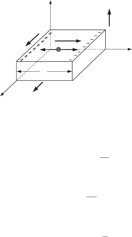
m (see Fig. C.12).
Reasoning. The current density of charge carriers is related to their concentration and
velocity by
j
x
= nqv
x
. (C.116)
From the last expression we can find the carrier velocity:
v
x
=
j
x
nq
. (C.117)
C.6 Electrons in semiconductors 411
F
e
z
x
y
B
E
j
F
m
e
E
H
L
Figure C.12 The Hall
effect.
The Hall effect is the occurrence of a transverse (with respect to the current direction)
voltage in a sample placed in perpendicular electric and magnetic fields (i.e., B ⊥ E). This
voltage can be found from the condition that, when the current flows along the x-direction,
the electric force, F
e
= qE
H
, and magnetic force, F
m
= qv ×B = j
x
B/n, which affect
the carriers counterbalance each other, i.e.,
qE
H
=
j
x
B
n
, (C.118)
where E
H
is the electric field intensity of the transverse Hall field. Taking into account
that E
H
= ϕ
H
/L, we obtain
E
H
=
ϕ
H
L
= R
H
j
x
B, (C.119)
where the Hall constant is equal to R
H
= 1/(nq). For the semiconductors with their
different types of carriers we have
R
H
=±
1
ne
, (C.120)
where e is the modulus of the electron charge. Using the values of n and e, we obtain
R
H
= 6.25 × 10
−3
m
3
C
−1
and ϕ
H
= 3.1 × 10
−3
V. By finding the sign of the Hall
constant, i.e., the direction of the Hall voltage, we can find the type of current carrier in
semiconductors. Note that Fig. C.12 corresponds to charge of carriers q = e > 0.
C.6 Electrons in semiconductors
C.6.1 Intrinsic and extrinsic conductivity
Semiconductors are a special group of crystals. These materials have such a name because
their resistivity is intermediate between those of dielectrics and metals. Thus, at room
temperature the resistivity of metals is ρ ≈ 10
−8
m; for dielectrics the magnitude of
this quantity is in the interval 10
12
−10
20
m; whereas for semiconductors this quantity
412 Appendix C. Crystals as atomic lattices
is in the interval 10
−4
−10
7
m (pure germanium, Ge, has ρ ≈ 0.5 m). The materials
which have semiconductor properties can be divided into two groups. The first group
includes the so-called “elemental” semiconductors, which consist of atoms of only one
element. The second group includes semiconductor compounds, which consist of atoms
of two or more types.
The main representatives of the first group are semiconductors such as silicon, Si,
whose atomic number is Z = 14, and germanium, Ge, whose atomic number is Z = 32.
Both elements have four valence electrons on their outermost shell. The crystalline lat-
tices of these semiconductors consist of atoms surrounded by four neighboring atoms,
each of which is bound to a particular atom by covalent two-electron bonds. Therefore,
in contrast to metals, whose valence electrons in a crystalline lattice become free, in
semiconductors at T = 0 K there are no free carriers. This makes a semiconductor have
the properties of a dielectric. However, there is a significant difference between semi-
conductors and dielectrics. The energy which is necessary to break the electron bond is
defined by the width of the bandgap, E
g
, which for different types of semiconductors
ranges from 0.01 eV to 2 eV, is significantly smaller than that in dielectrics. For com-
parison, the width of the bandgap in Si is equal to E
g
= 1.1eVandinGeE
g
= 0.7 eV,
whereas good dielectrics have E
g
of about several electron-volts (for example, diamond has
E
g
= 5.4 eV).
The second group of semiconductor materials is large. We can mention first of all
binary compounds of elements of the third and fifth groups of the Periodic Table of the
elements (for example, GaAs and InSb). These compounds are usually denoted as A
3
B
5
and their properties are very similar to those of “elemental” semiconductors from the first
group. Binary semiconductors also include A
2
B
6
compounds (for example, ZnS), metal
oxides (for example, Cu
2
O), and organic compounds.
External influences on such semiconductors (for example, heating or exposure to
radiation) may detach some of the electrons from atoms and free them. This means that
these electrons from the valence band move to the conduction band, where they occupy the
lowest levels. Being in the conduction band, electrons in an external electric field behave
as the electrons in a metal would, i.e., they participate in the directed transfer of charge.
Simultaneously with the appearance of electrons in the conduction band, vacancies are
formed in the valence band, which are called holes, i.e., not completely occupied levels.
These levels may, because of external influences, be occupied by the electrons residing
on the lower energy levels of a valence band. The direction of a displacement of these
electrons in a valence band under the influence of an external electric field is equivalent
to the direction of a displacement of positively charged holes. Thus, the existence of
holes makes additional input to the electrical conductivity of a semiconductor. Its total
conductivity is composed from electron and hole conductivities and, taking into account
that the concentration of electrons, n
n
, in the conduction band and that of holes, n
p
,inthe
valence band are equal to each other, the conductivity can be written as
σ = q
n
n
n
µ
n
+q
p
n
p
µ
p
, (C.121)
where q
n
,µ
n
and q
p
,µ
p
are the charge and mobility of electrons and holes, respectively.
The electron and hole mobilities are similar in magnitude despite the motion of a hole being
a peculiar “relay-race” motion of many electrons. Therefore, we can assume that the total
conductivity is approximately twice the electron conductivity. This type of conductivity is