Neamen D. Microelectronics: Circuit Analysis and Design
Подождите немного. Документ загружается.


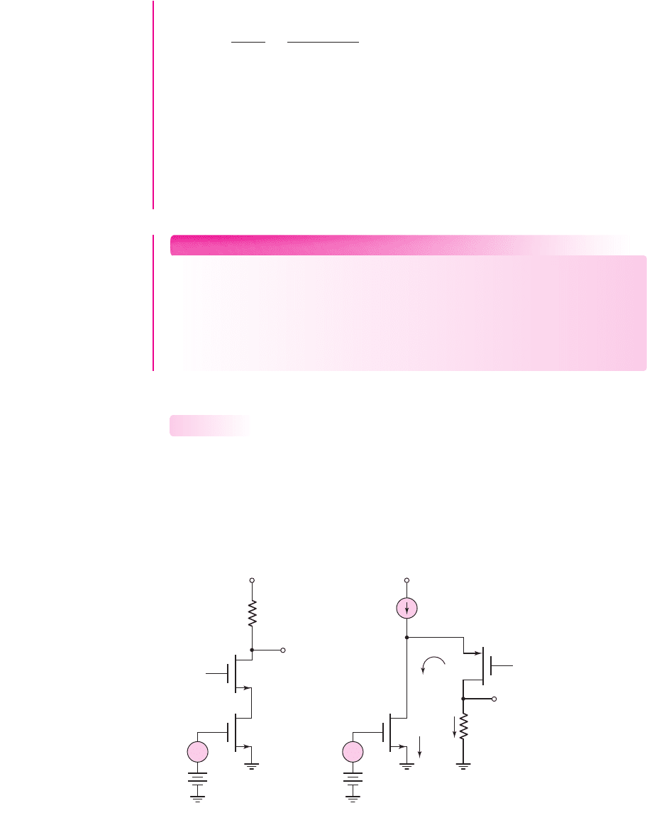
Comment: We showed previously that the output resistance of an emitter-follower
circuit is low. For comparison, typical output resistance values for the 741 op-amp
are
75
. This correlates well with our analysis.
EXERCISE PROBLEM
Ex 13.6: Repeat Example 13.6 assuming Early voltages of
V
A
= 100
V. (Ans.
R
o
= 90.9
)
Frequency Response
The 741 op-amp is internally compensated by the Miller compensation technique to
introduce a dominant low-frequency pole. From Miller’s theorem, the effective input
capacitance of the second gain stage is
C
i
= C
1
(1 +
|
A
v2
|
)
(13.30)
The dominant low-frequency pole is
f
PD
=
1
2π R
eq
C
i
(13.31)
where
R
eq
is the equivalent resistance between the second-stage input node and
ground, and is
R
eq
= R
o1
R
i2
(13.32)
Here R
i2
is the input resistance of the gain stage and R
o1
is the output resistance of the
diff-amp stage. From Figure 13.10, we see that
R
o1
= R
act1
r
o4
(13.33)
EXAMPLE 13.7
Objective: Determine the dominant-pole frequency of the 741 op-amp.
Use appropriate results from previous calculations.
Solution: Previously, we determined that
|
A
v2
|
= 285
, which means that the effec-
tive input capacitance is
C
i
= C
1
(1 +
|
A
v2
|
) = (30)(1 +285) = 8580 pF
The gain stage input resistance was found to be
R
i2
= 4.07 M
. We find
R
o1
= R
act1
r
o4
= 7.185.26 = 3.04 M
The equivalent resistance is then
R
eq
= R
o1
R
i2
= 3.044.07 = 1.74 M
Finally, the dominant-pole frequency is
f
PD
=
1
2π R
eq
C
i
=
1
2π(1.74 ×10
6
)(8580 × 10
−12
)
= 10.7Hz
Comment: The very large equivalent input capacitance
C
i
justifies neglecting any
other capacitance effects at the gain stage input.
13.2.4
968 Part 2 Analog Electronics
nea80644_ch13_947-1008.qxd 6/23/09 1:59 PM Page 968 pmath DATA-DISK:Desktop Folder:23/06/09:MHDQ134-13:

EXERCISE PROBLEM
Ex 13.7: Repeat Example 13.7 assuming Early voltages of
V
A
= 100
V. See
Exercise Problems Ex 13.4, Ex 13.5, and Ex 13.6. (Ans. 3.88 Hz)
If all other poles of the op-amp circuit are at very high frequencies, then the
unity-gain bandwidth is
f
T
= A
o
f
PD
(13.34)
Using our results, we find that
f
T
= (181,260)(10.7)
∼
=
1.9 MHz
(13.35)
A typical unity-gain bandwidth value for the 741 op-amp is 1 MHz. With all the
approximations and assumptions, such as the value of reverse saturation current and
Early voltage, used in the calculations, a factor of two between the actual and pre-
dicted cutoff frequency is not significant.
If the frequencies of the other poles of the 741 op-amp are greater than 1.9 MHz,
the phase margin is 90 degrees. This phase margin ensures that any closed-loop am-
plifier circuit using the 741 op-amp will be stable for any feedback transfer function.
Problem-Solving Technique: Operational Amplifier Circuits
1. DC analysis. The bias portion of the op-amp circuit must be identified. A
reference current must be determined and then the bias currents in the indi-
vidual building blocks of the overall circuit can be determined.
2. AC analysis. The small-signal properties of the building blocks of the overall
circuit can be analyzed individually, provided that the loading effects of
follow-on stages are taken into account.
Test Your Understanding
TYU 13.3 Using the results of Example 13.1 and assuming
β
n
= 200
, determine the
input base currents to
Q
1
and
Q
2
. (Ans.
I
B1
= I
B2
= 47.5
nA)
TYU 13.4 The 741 op-amp in Figure 13.3 is biased at
V
+
= 15
V and
V
−
=−15
V.
Assume
V
BE
(npn) = V
EB
(pnp) = 0.6
V. Determine the input common-mode voltage
range, neglecting voltage drops across R
1
and R
2
. (Ans.
−12.6 <v
in
(cm)
≤ 14.4
V)
TYU 13.5 (a) If the 741 op-amp in Figure 13.3 is biased at
V
+
=15
and
V
−
=−15
V,
estimate the maximum and minimum output voltages such that the op-amp remains
biased in its linear region. (b) Repeat part (a) if
V
+
= 5
V and
V
−
=−5
V. (Ans.
(a)
−13.2 ≤ v
O
≤ 13.8
V (b)
−3.2 ≤ v
O
≤ 3.8
V)
TYU 13.6 Consider the input stage and bias circuit in Figure 13.5 with supply volt-
ages
V
+
= 5
V and
V
−
=−5
V. If
I
S
= 5 ×10
−15
A for each transistor, determine
I
REF
,
V
BE11
,
V
BE10
,
V
BE6
, and
I
C10
. (Ans.
I
REF
= 0.218
mA,
V
BE11
= 0.637
V,
I
C10
= 14.2 μ
A,
V
BE10
= 0.566
V,
V
BE6
= 0.548
V)
TYU 13.7 The power supply voltages for the 741 op-amp in Figure 13.3 are
V
+
= 10 V
and
V
−
=−10 V
. Neglect base currents and assume
V
BE
(npn) =
V
EB
(pnp) = 0.6V
. Calculate the bias currents
I
REF
,
I
C10
,
I
C6
,
I
C13B
, and
I
C13A
.
Chapter 13 Operational Amplifier Circuits 969
nea80644_ch13_947-1008.qxd 6/23/09 1:59 PM Page 969 pmath DATA-DISK:Desktop Folder:23/06/09:MHDQ134-13:

(Ans.
I
REF
= 0.47 mA
,
I
C10
= 17.2 μA
,
I
C6
= 8.6 μA
,
I
C13B
= 0.353 mA
,
I
C13A
= 0.118 mA
)
*TYU 13.8 In the 741 op-amp output stage in Figure 13.3, the combination of Q
18
,
Q
19
, and R
10
is replaced by two series diodes with
I
S
= 10
−14
A. The transistor
parameters are:
β
n
= 200
,
β
p
= 50
, and
V
A
= 50
V. Assume the same dc bias
currents calculated previously. Calculate the output resistance, assuming Q
14
is con-
ducting, producing a load current of 5 mA. (Ans. 41
)
13.3 CMOS OPERATIONAL AMPLIFIER CIRCUITS
Objective: • Describe and analyze the dc and ac characteristics of
CMOS operational amplifier circuits.
The 741 bipolar op-amp is a general-purpose op-amp capable of sourcing and sink-
ing reasonably large load currents. The output stage is an emitter follower capable of
supplying the necessary load current, with a low output resistance to minimize load-
ing effects.
In contrast, most CMOS op-amps are designed for specific on-chip applications
and are only required to drive capacitive loads of a few picofarads. Most CMOS
op-amps therefore do not need a low-resistance output stage, and, if the op-amp in-
puts are not connected directly to the IC external terminals, they also do not need
electrostatic input protection devices.
In this section, we consider four designs of a CMOS op-amp. Initially we con-
sider a simple CMOS design to begin to understand the basic concepts of a CMOS
op-amp. We then analyze a three-stage CMOS op-amp with a complementary push-
pull output stage. The third CMOS op-amp is a more sophisticated design, called a
folded cascode op-amp. Finally, we consider a current-mirror CMOS op-amp. In
each case, we will do a dc analysis/design and a small-signal analysis/design.
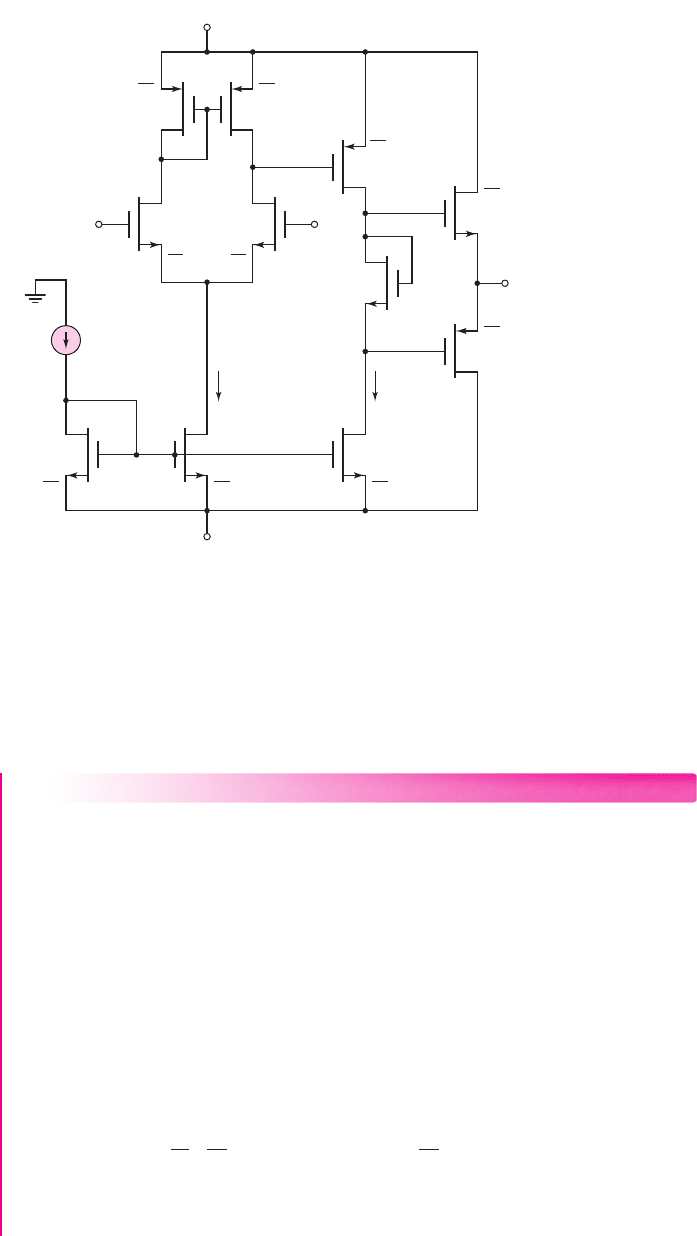
MC14573 CMOS Operational Amplifier Circuit
Circuit Description
An example of an all-CMOS op-amp is the MC14573, for which a simplified circuit
diagram is shown in Figure 13.14. The p-channel transistors M
1
and M
2
form the
input differential pair, and the n-channel transistors M
3
and M
4
form the active load.
The diff-amp input stage is biased by the current mirror M
5
and M
6
, in which the
reference current is determined by an external resistor R
set
.
The second stage, which is also the output stage, consists of the common-source-
connected transistor M
7
. Transistor M
8
provides the bias current for M
7
and acts as the
active load. An internal compensation capacitor C
1
is included to provide stability.
DC Analysis
Assuming transistors M
5
and M
6
are matched, the reference and input-stage bias
currents are given by
I
set
= I
Q
=
V
+
− V
−
− V
SG5
R
set
(13.36)
13.3.1
970 Part 2 Analog Electronics
nea80644_ch13_947-1008.qxd 6/23/09 1:59 PM Page 970 pmath DATA-DISK:Desktop Folder:23/06/09:MHDQ134-13:

The reference current and source-to-gate voltage are also related by
I
set
= K
p5
(V
SG5
+ V
TP
)
2
(13.37)
where
V
TP
and
K
p5
are the threshold voltage and conduction parameter of the
p-channel transistor M
5
.
EXAMPLE 13.8
Objective: Determine the dc bias currents in the MC14573 op-amp.
Assume transistor parameters of
|
V
T
|
= 0.5
V (all transistors),
k
n
= 100 μ
A/V
2
,
k
p
= 40 μ
A/V
2
, and circuit parameters of
V
+
= 5
V,
V
−
=−5
V, and
R
set
= 225
k
.
Assume transistor width-to-length ratios of 6.25 for
M
3
and
M
4
, and 12.5 for all other
transistors.
Solution: For transistors
M
5
and
M
6
, the conduction parameters are:
K
p
=
k
p
2
W
L
5
=
0.04
2
(
12.5
)
= 0.25
mA/V
2
Combining Equations (13.36) and (13.37) yields the source-to-gate voltage of
M
5
:
K
p
(
V
SG5
+ V
TP
)
2
=
V
+
− V
SG5
− V
−
R
set
or
0.25
(
V
SG5
−0.5
)
2
=
5 − V
SG5
−
(
−5
)
225
which yields
V
SG5
= 0.9022
V
Chapter 13 Operational Amplifier Circuits 971
V
–
V
+
v
1
v
2
C
1
v
o
R
set
M
6
M
1
M
2
M
8
M
5
I
Q
I
set
M
3
M
4
M
7
4
Figure 13.14 MC14573 CMOS op-amp equivalent circuit
nea80644_ch13_947-1008.qxd 6/23/09 1:59 PM Page 971 pmath DATA-DISK:Desktop Folder:23/06/09:MHDQ134-13:

From Equation (13.36), we have
I
set
= I
Q
=
10 − 0.9022
225
⇒ 40.4 μA
The quiescent drain currents in
M
7
and
M
8
are then also
40.4 μ
A, and the currents in
M
1
through
M
4
are
20.2 μ
A.
Comment: The quiescent bias currents can be changed easily by changing the external
resistor R
set
. Transistors M
5
, M
6
, and M
8
are identical, so the currents in these three
devices are equal since the source-to-gate voltages are the same. The width-to-length
ratio of M
7
is twice that of M
3
and M
4
, which means the current in M
7
is twice that in
M
3
and M
4
. However, this is consistent with the current-source transistor currents.
EXERCISE PROBLEM
Ex 13.8: Repeat Example 13.8 assuming transistor width-to-length ratios of
(W/L)
3,4
= 10
for transistors
M
3
and
M
4
, and
W/L = 20
for all other transistors.
Let
R
set
= 150 k
. (Ans.
I
REF
= I
Q
= I
D7
= I
D8
= 60.74 μ A, I
D1
− I
D4
=
30.37 μ
A)
Small-Signal Analysis
The small-signal differential voltage gain of the input stage can be written as
A
d
= g
m
(
r
o2
r
o4
)
= 2
K
p1
I
DQ1
(
r
o2
r
o4
)
=
2K
p1
I
Q
(
r
o2
r
o4
)
(13.38)
where r
o2
and r
o4
are the output resistances of M
2
and M
4
, respectively. The input
impedance to the second stage is essentially infinite; therefore, there is no loading
effect due to the second stage. If we assume that the parameter
λ
is the same for all
transistors, then
r
o2
= r
o4
=
1
λI
D
(13.39)
where I
D
, which is the quiescent drain current in M
2
and M
4
, is
I
D
= I
Q
/2
.
The magnitude of the gain of the second stage is
A
v2
= g
m7
(
r
o7
r
o8
)
(13.40)
where
g
m7
= 2
K
n7
I
D7
and
r
o7
= r
o8
= 1/λI
D7
Equation (13.40) implies that there is no loading effect due to an external load con-
nected at the output.
EXAMPLE 13.9
Objective: Determine the small-signal voltage gains of the input and second stages,
and the overall voltage gain, of the MC14573 op-amp.
Assume the same transistor and circuit parameters as in Example 13.8. Let
λ = 0.02 V
−1
for all transistors.
972 Part 2 Analog Electronics
nea80644_ch13_947-1008.qxd 6/23/09 1:59 PM Page 972 pmath DATA-DISK:Desktop Folder:23/06/09:MHDQ134-13:

Solution: The conduction parameters of
M
1
and
M
2
are
K
p1
= K
p2
=
k
p
2
W
L
1
=
0.04
2
(
12.5
)
= 0.25
mA/V
2
and the output resistances are
r
o2
= r
o4
=
1
λI
D2
=
1
(0.02)(0.0202)
⇒ 2.475 M
From Equation (13.38), the differential voltage gain of the input stage is then
A
d
=
2K
p1
I
Q
(
r
o2
r
o4
)
=
√
2
(
0.25
)(
0.0404
)
(2475
2475)
or
A
d
= 176
The transconductance of
M
7
is
g
m7
= 2
k
n
2
W
L
7
I
D7
= 2
0.1
2
(
12.5
)(
0.0404
)
= 0.3178
mA/V
and the output resistances of
M
7
and
M
8
are
r
o7
= r
o8
=
1
λI
D7
=
1
(0.02)(0.0404)
⇒ 1.238 M
From Equation (13.40), the magnitude of the voltage gain of the second stage is then
A
v2
= g
m7
(
r
07
r
08
)
=
(
0.3178
)(
1238
1238
)
= 197
Finally, the overall voltage gain magnitude of the op-amp is
A
v
= A
d
A
v2
= (176)(197) = 34,672
Comment: The calculated overall voltage gain is 91 dB, which correlates very well
with typical values of 90 dB, as listed in the data sheet for the MC14573 op-amp. The
open-loop gain of a CMOS op-amp is generally less than that of a bipolar op-amp,
but the use of active loads provides acceptable results.
EXERCISE PROBLEM
Ex 13.9: Repeat Example 13.9 using circuit and transistor parameters given in
Exercise Ex 13.8. (Ans.
A
d
= 181.4
,
A
v2
= 202.9
,
A
v
= 91.3
dB)
Three-Stage CMOS Operational Amplifier
Figure 13.15 shows a three-stage CMOS op-amp circuit. The differential input stage
consists of the differential pair M
1
and M
2
with active load transistors M
3
and M
4
. The
input stage is biased with the constant-current source M
10
and M
11
. As shown in Chap-
ter 10, the reference current can be established with additional NMOS transistors.
The output of the input stage is connected to the common-source amplifier con-
sisting of M
5
. The transistor M
9
establishes the bias current I
Q2
and also acts as the
active load for the common-source amplifier.
13.3.2
Chapter 13 Operational Amplifier Circuits 973
nea80644_ch13_947-1008.qxd 6/23/09 1:59 PM Page 973 pmath DATA-DISK:Desktop Folder:23/06/09:MHDQ134-13:
Transistors M
6
and M
7
form the complementary push–pull output stage. Tran-
sistor M
8
acts as a resistor and provides a potential difference between the gates of
the output transistors to minimize crossover distortion in the output signal.
Example width-to-length ratios of the transistors in the CMOS op-amp circuit
are shown in the figure. These ratios will be used in the following example.
EXAMPLE 13.10
Objective: Determine the dc and ac characteristics of a three-stage CMOS op-amp.
Consider the three-stage CMOS op-amp shown in Figure 13.15. The NMOS
transistor parameters are
V
TN
= 0.7
V,
k
n
= 80 μA/V
2
,
λ
n
= 0.01 V
−1
, and the
PMOS transistor parameters are
V
TP
=−0.7
V,
k
p
= 40 μA/V
2
,
λ
p
= 0.015 V
−1
.
Assume the reference current is
I
REF
= 160 μA
.
Solution (DC Analysis): Since M
9
, M
10
, and M
11
are matched transistors, then
I
Q1
= I
Q2
= I
REF
= 160 μA
.
Transistors M
3
and M
4
are matched so that in the quiescent condition,
V
SG3
=
V
SD3
=V
SD4
. Since
V
SG5
=V
SD4
and since the current in
M
5
is twice as large as that
in
M
4
, the width-to-length ratio of
M
5
must be twice as large as that of M
3
and M
4
.
If we provide dc biases of
V
GS6
= V
SG7
= 0.85
V to the output transistors, then
the dc quiescent current in the output transistors will be
I
D6
= I
D7
=
k
n
2
W
L
6
(
V
GS6
− V
TN
)
2
=
80
2
(25)(0.85 − 0.7)
2
or
I
D6
= I
D7
= 22.5 μA
974 Part 2 Analog Electronics
I
Q1
v
1
v
2
v
o2
v
o1
v
o
I
REF
I
Q2
M
10
M
9
M
8
M
5
M
4
M
3
M
2
M
1
M
7
M
6
M
11
20
1
20
1
20
1
50
1
25
1
80
1
V
+
= 5 V
V
–
= –5 V
40
1
40
1
15
1
15
1
Figure 13.15 A three-stage CMOS operational amplifier
nea80644_ch13_947-1008.qxd 6/23/09 1:59 PM Page 974 pmath DATA-DISK:Desktop Folder:23/06/09:MHDQ134-13:

The potential difference across M
8
must then be
V
DS8
= 2(0.85) = 1.7
V. We
then have
I
D8
= I
Q2
= 160 =
80
2
W
L
8
(
1.7 − 0.7
)
2
which yields a required width-to-length ratio of
(W/L)
8
= 4
.
Solution (AC Analysis): Since there is no loading effect between stages of the
CMOS op-amp, we can write the overall differential voltage gain as
A
v
= A
d1
A
2
A
3
where the gains A
d1
, A
2
, and A
3
are the voltage gains of each individual stage. Since
the output stage is a source-follower circuit, we can write that
A
3
∼
=
1
.
Defining the differential input voltage as
v
d
= v
1
−v
2
, the differential voltage
gain of the input stage (using results from Chapter 11) is
A
d1
=
v
o1
v
d
= g
m1
(r
o2
r
o4
)
We find
g
m1
= 2
k
n
2
W
L
1
I
Q1
2
= 2
0.08
2
(15)
0.16
2
or
g
m1
= 0.438 mA/V
Also
r
o2
=
1
λ
n
(I
Q1
/2)
=
1
(0.01)(0.08)
= 1250 k
and
r
o4
=
1
λ
p
(I
Q1
/2)
=
1
(0.015)(0.08)
= 833.3k
We then find
A
d1
= (0.438)(1250833.3) = 219
The resistance of M
8
is relatively small, so the voltage gain of the second common-
source stage is given by
A
2
=−g
m5
(r
o5
r
o9
)
We find
g
m5
= 2
k
p
2
W
L
5
I
Q2
= 2
0.04
2
(80)(0.16)
or
g
m5
= 1.012 mA/V
Also
r
o5
=
1
λ
p
I
Q2
=
1
(0.015)(0.16)
= 416.7k
Chapter 13 Operational Amplifier Circuits 975
nea80644_ch13_947-1008.qxd 6/23/09 1:59 PM Page 975 pmath DATA-DISK:Desktop Folder:23/06/09:MHDQ134-13:
and
r
o9
=
1
λ
n
I
Q2
=
1
(0.01)(0.16)
= 625 k
The voltage gain of the second stage is then
A
2
=−(1.012)(416.7625) =−253
The overall differential voltage gain of this three-stage CMOS op-amp is then
A
v
= A
d1
A
2
= (219)(−253) =−55,407
Comment: A reasonable differential voltage gain is obtained in this three-stage
CMOS amplifier.
EXERCISE PROBLEM
Ex 13.10: (a) Calculate the differential voltage gains of the first and second stages,
and the overall voltage gain of the three-stage CMOS op-amp in Figure 13.15 if
(W/L)
1,2
= 22.5
and
I
REF
= 200 μ
A. All other parameters are the same as given
in Example 13.10. (b) Recalculate
(W/L)
8
if the quiescent current in the output
transistors is to be 40
μ
A. (Ans. (a)
A
d
= 240
,
A
2
=−226.2
,
A =−54, 288
;
(b)
(W/L)
8
= 4.13)
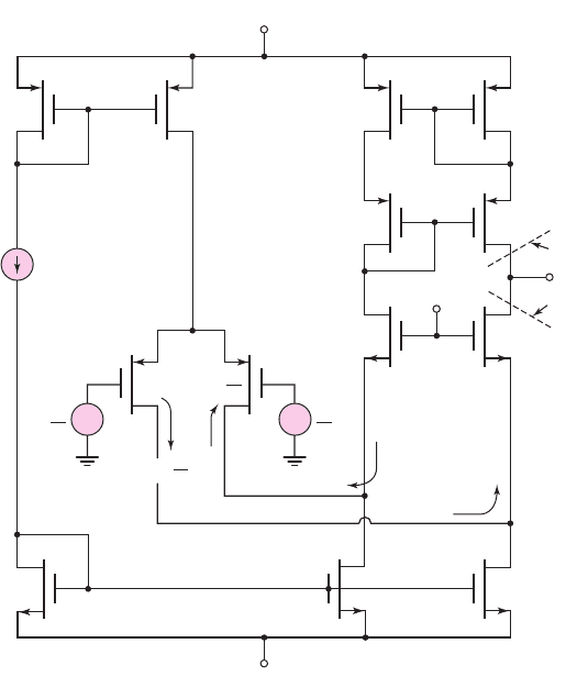
Folded Cascode CMOS Operational
Amplifier Circuit
As we have mentioned previously, the voltage gain of an amplifier can be increased
by using a cascode configuration. In its simplest form, the conventional cascode
configuration consists of two transistors in series, as shown in Figure 13.16(a). The
13.3.3
976 Part 2 Analog Electronics
~ ~
V
DD
R
L
I
Q
R
L
V
B2
V
B3
+
–
V
B1
+
–
V
B1
M
2
M
2
i
sig
M
1
M
1
I
1
I
2
v
o
v
o
v
i
v
i
V
DD
(a) (b)
Figure 13.16 (a) Classical cascode stage. (b) folded-cascode stage
nea80644_ch13_947-1008.qxd 6/23/09 1:59 PM Page 976 pmath DATA-DISK:Desktop Folder:23/06/09:MHDQ134-13:
transistor M
1
is the common-source amplifying device whose current is determined
by the input voltage. This current is the input signal to M
2
, which is connected in a
common-gate configuration. The output is taken off the drain of the cascode tran-
sistor. The circuit in Figure 13.16(b) has a slightly different configuration. The dc
current I
1
in M
1
is determined by the input voltage. The dc current in M
2
is the
difference between the bias current I
Q
and I
1
.
The ac current in the conventional cascode circuit of Figure 13.16(a) is through
both transistors and the dc power supply. The ac current in the cascode circuit in Fig-
ure 13.16(b) is through both transistors and ground as indicated in the figure. The ac
current in M
2
of this circuit is equal in magnitude but in the opposite direction to M
1
.
Thus the current is said to be folded back and the circuit in Figure 13.16(b) is called
a folded cascode circuit.
The folded cascode configuration can be applied to the diff-amp as shown in
Figure 13.17. The transistors M
1
and M
2
are the differential pair, as usual, and tran-
sistors M
5
and M
6
are the cascode transistors. Transistors M
7
–M
10
form a modified
Wilson current mirror acting as an active load. This configuration was discussed in
Chapter 10.
Assuming that transistors M
3
, M
4
, and M
11
–M
13
are all matched, then the dc cur-
rents in M
1
and M
2
are I
REF
/2 and those in M
3
and M
4
are I
REF
. This means that the
dc currents in the cascode transistors M
5
and M
6
are I
REF
/2.
Chapter 13 Operational Amplifier Circuits 977
+
–
–
+
v
d
2
v
d
2
R
o6
R
o8
V
B2
V
+
V
–
M
1
v
1
v
2
M
2
M
3
M
13
M
4
M
6
M
5
M
7
M
9
M
11
I
REF
M
12
M
10
M
8
i
i
v
d
2
i = g
m
v
d
2
i = g
m
v
o
Figure 13.17 CMOS folded cascode amplifier
nea80644_ch13_947-1008.qxd 6/23/09 1:59 PM Page 977 pmath DATA-DISK:Desktop Folder:23/06/09:MHDQ134-13: