Neamen D. Microelectronics: Circuit Analysis and Design
Подождите немного. Документ загружается.


Overall Gain
Since we have taken the loading effects of each following stage into account, the
overall voltage gain is the product of the individual gain factors, or
A
v
= A
d
A
v2
A
v3
(13.59)
where
A
v3
is the voltage gain of the output stage. If we assume that
A
v3
∼
=
1
for the
emitter-follower output stage, then the overall gain of the CA3140 op-amp is
A
v
= A
d
A
v2
A
v3
= (12.7)(1923)(1) = 24,422
(13.60)
Typical values of the gain of the CA3140 op-amp are in the area of 100,000;
thus, our calculations give a somewhat smaller value.
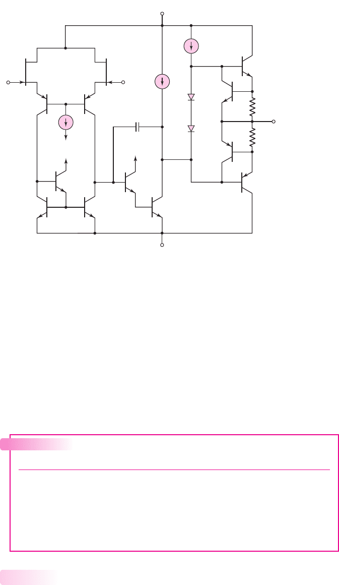
Frequency Response
The CA3140 op-amp is internally compensated by the Miller compensation tech-
nique to introduce a dominant pole, as was done in the 741 op-amp. The feedback
capacitor C
1
is 12 pF and is connected between the collector and the base of Q
13
, as
shown in Figure 13.20. From Miller’s theorem, the effective input capacitance of the
second stage is
C
i
= C
1
(1 +|A
v2
|)
(13.61)
The low-frequency dominant pole is
f
PD
=
1
2π R
eq
C
i
(13.62)
where R
eq
is the equivalent resistance between the second-stage input node and
ground. Since this resistance is dominated by the input resistance to Q
13
, we have
R
eq
∼
=
R
i2
= r
π13
(13.63)
EXAMPLE 13.15
Objective: Determine the dominant-pole frequency and unity-gain bandwidth of the
CA3140 op-amp.
Again, we will use results from previous calculations.
Solution: Previously, we determined that
|A
v2
|=1923
; therefore, the effective
input capacitance is
C
i
= C
1
(1 +|A
v2
|) = 12(1 +1923) = 23,088 pF
The gain stage input resistance is
R
i2
= r
π13
= 26 k
which means that
f
PD
∼
=
1
2π R
i2
C
i
=
1
2π(26 ×10
3
)(23,088 × 10
−12
)
= 265 Hz
Finally, the unity-gain bandwidth is
f
T
= f
PD
A
v
= (265)(24,422) ⇒ 6.47 MHz
Comment: This unity-gain bandwidth value compares favorably with typical values
of 4.5 MHz listed in the data sheet.
988 Part 2 Analog Electronics
nea80644_ch13_947-1008.qxd 6/23/09 1:59 PM Page 988 pmath DATA-DISK:Desktop Folder:23/06/09:MHDQ134-13:

EXERCISE PROBLEM
Ex 13.15: If the gain of the input stage of the CA3140 op-amp is increased to
A
d
= 16.4
, determine the unity-gain bandwidth. All other parameters are the
same as given in Example 13.15. (Ans.
f
T
= 8.32
MHz)
Test Your Understanding
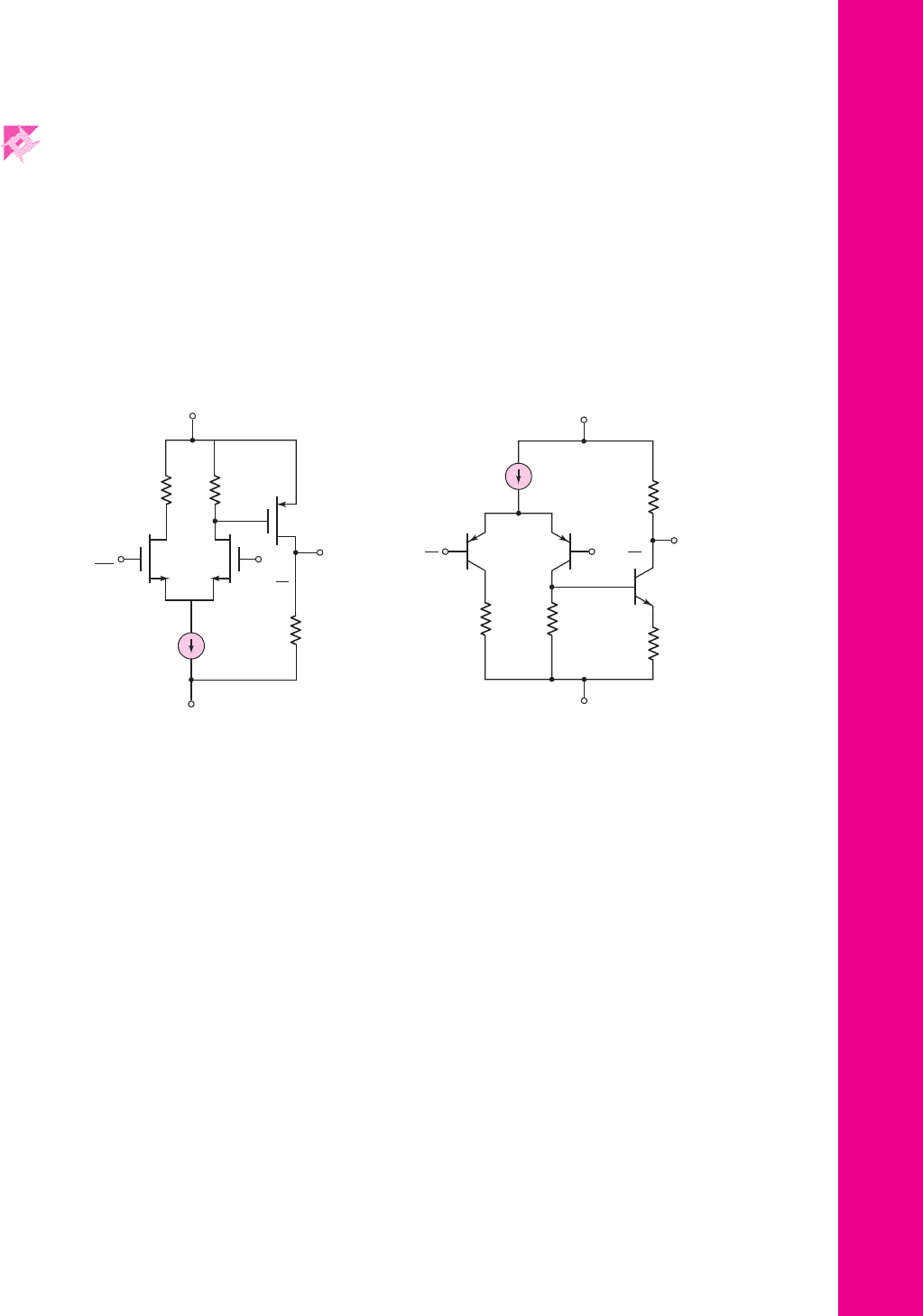
TYU 13.14 Consider the BiCMOS folded cascode amplifier in Figure 13.20. As-
sume the circuit and MOS transistor parameters are the same as in Example 13.11.
Assume BJT parameters of
β = 120
and
V
A
= 80
V. (a) Determine the small-signal
voltage gain. (b) If the effective capacitance at the output node is 2 pF, determine
the dominant-pole frequency and the gain–bandwidth product. (Ans. (a) 76,343,
(b) 329 Hz, 25.1 MHz)
TYU 13.15 Consider the CA3140 op-amp bias circuit in Figure 13.22. Assume
that
V
BE7
= 0.6
V and
R
1
= 5k
. If the p-channel MOSFET parameters are
K
p
= 0.3 mA/V
2
and
|
V
TP
|
= 1.4V
, determine I
1
, I
2
, and
V
SG
. (Ans.
V
SG
= 2.54
V,
I
1
= I
2
= 0.388
mA)
13.5 JFET OPERATIONAL AMPLIFIER CIRCUITS
Objective: • Describe the characteristics of two hybrid JFET opera-
tional amplifier circuits.
The advantage of using MOSFETs as input devices in a BiCMOS op-amp is that ex-
tremely small input bias currents can be achieved. However, MOSFET gates con-
nected to outside terminals of an IC must be protected against electrostatic damage.
Typically, this is accomplished by using back-biased diodes on the input, as was
shown in Figure 13.21. Unfortunately, the input op-amp bias currents are then dom-
inated by the leakage currents in the protection diodes, which means that the small
input bias currents cannot be fully realized. JFETs as input devices also offer the ad-
vantage of low input currents, and they do not need electrostatic protection devices.
Input gate currents in a JFET are usually well below 1 nA, and are often on the order
of 10 pA. In addition, JFETs offer greatly reduced noise properties.
In this section, we will examine two op-amp configurations using JFETs as input
devices. Since the analysis is essentially identical to that given in the last two sec-
tions, we will limit ourselves to a general discussion of the circuit characteristics.
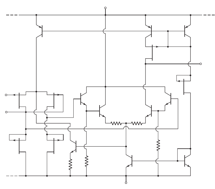
Hybrid FET Op-Amp, LH002/42/52 Series
Figure 13.24 is a simplified circuit diagram of an LH002/42/52 series op-amp, which
uses a pair of JFETs for the input differential pair. Note that the general layout of the
circuit is essentially the same as that of the 741 op-amp.
The input diff-amp stage consists of transistors J
1
, J
2
, Q
3
, and Q
4
; J
1
and J
2
are
n-channel JFETs operating in a source-follower configuration. The differential output
13.5.1
Chapter 13 Operational Amplifier Circuits 989
nea80644_ch13_947-1008.qxd 6/23/09 1:59 PM Page 989 pmath DATA-DISK:Desktop Folder:23/06/09:MHDQ134-13:
signal from J
1
and J
2
is the input to the common-base amplifier formed by Q
3
and Q
4
,
which provides a large voltage gain. Transistors Q
5
, Q
6
, and Q
7
form the active load
for the input stage.
The gain stage is composed of Q
16
and Q
17
connected in a Darlington pair
configuration. This stage also includes a 30 pF compensation capacitor. The output
stage consists of the complementary push–pull emitter-follower configuration of Q
14
and Q
20
. Transistors Q
14
and Q
20
are biased slightly “on” by diodes Q
10
and Q
19
, to
minimize crossover distortion. Transistors Q
15
and Q
21
and the associated 27
and
22
resistors provide the short-circuit protection.
An abbreviated data sheet for an LH0042C op-amp is shown in Table 13.3. Note
the very large differential-mode input resistance and the low input bias current.
990 Part 2 Analog Electronics
V
–
V
–
Q
19
Q
10
Q
5
Q
6
Q
17
J
1
J
2
V
+
V
+
V
+
Q
7
Q
16
Q
3
Q
4
C
C
= 30 pF
27 Ω
Q
14
22 Ω
Q
15
Q
21
Q
20
–
+
Output
Figure 13.24 Equivalent circuit, LH0022/42/52 series hybrid JFET op-amp
Table 13.3 LH0042C data
Parameter Minimum Typical Maximum Units
Input bias current 15 50 pA
Differential-mode input 10
12
resistance
Input capacitance 4 pF
Open-loop gain (R
L
=
1 k
) 25,000 100,000 V/V
Unity-gain frequency 1 MHz
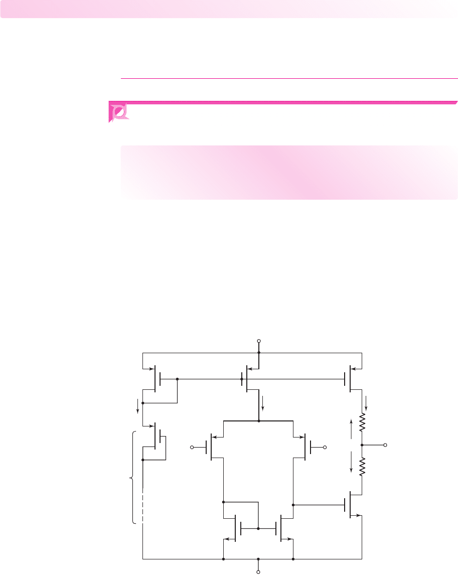
Hybrid FET Op-Amp, LF155 Series
Another example of a JFET op-amp is the LF155 BiFET op-amp. A simplified circuit
diagram showing the input stage is in Figure 13.25. The input BiFET op-amp stage
13.5.2
nea80644_ch13_947-1008.qxd 6/23/09 1:59 PM Page 990 pmath DATA-DISK:Desktop Folder:23/06/09:MHDQ134-13:
consists of p-channel JFETs
J
1
and
J
2
biased by the bipolar transistor
Q
1
. The active
load for the input diff-amp consists of the p-channel JFETs
J
3
and
J
4
, for which
V
GS
= 0
.
A two-sided output from the input diff-amp stage is connected to a second diff-
amp stage consisting of Darlington pairs Q
7
through Q
10
. The second, or gain, stage
is biased by bipolar transistor Q
5
. The cascode configuration of J
5
and Q
2
form the
active load for the gain stage.
The circuit has a common-mode feedback loop in the bias circuit. The base of Q
6
is connected to the collector of Q
5
. If the drain voltages of J
1
and J
2
increase, the
Darlington second stage drives the base voltage of Q
6
higher. The current in Q
6
then
increases, reducing the drain currents in J
1
and J
2
, since I
C1
is a constant current.
Smaller drain currents cause the voltages at the J
1
and J
2
drains to decrease, which
then stabilizes the drain voltages.
JFET J
6
is connected as a current source, which establishes a reference current in
Q
3
, Q
4
, and J
6
. This reference current then produces the bias currents in the current
mirrors
Q
4
–
Q
5
and
Q
1
–
Q
2
–
Q
3
.
In this BiFET op-amp, we see the advantages of incorporating both JFET and
bipolars in the same circuit. The JFET input devices provide a very high input im-
pedance, normally in the range of 10
12
. The current-connected transistor J
6
allows
the reference bias current to be controlled without the use of a resistor. Incorporating
bipolar transistors in the second stage takes advantage of their higher transconduc-
tance values compared to JFETs, to produce a high second-stage gain.
Chapter 13 Operational Amplifier Circuits 991
R
2
=
5 kΩ
R
4
=
30 Ω
R
5
=
30 Ω
R
3
=
5 kΩ
R
1
=
1 kΩ
Q
1
J
1
J
2
J
3
J
4
Q
8
Q
7
Q
9
Q
10
J
6
Q
4
Q
5
Q
3
Q
2
J
5
Q
6
+
–
V
+
V
–
V
i
V
x
Figure 13.25 Equivalent circuit, LF155 BiFET op-amp input stages
nea80644_ch13_947-1008.qxd 6/23/09 1:59 PM Page 991 pmath DATA-DISK:Desktop Folder:23/06/09:MHDQ134-13:
Test Your Understanding
TYU 13.16 Consider the LF155 BiFET input stage in Figure 13.25. The p-channel
JFET parameters are
I
DSS
= 300 μA, V
p
= 1V
, and
λ = 0.01 V
−1
. The supply volt-
ages are
V
+
= 5V
and
V
−
=−5V
. Let
V
BE
(npn) = 0.6
V and
V
EB
(pnp) = 0.6
V.
Determine the bias currents
I
C3
, I
C2
, and
I
C1
. (Ans.
I
C1
= I
C2
= I
C3
= 300 μA
)
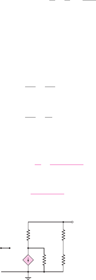
13.6 DESIGN APPLICATION: A TWO-STAGE CMOS
OP-AMP TO MATCH A GIVEN OUTPUT STAGE
Objective: • Design a two-stage CMOS op-amp that will match
the output stage in Figure 8.38 that was the design application in
Chapter 8.
Specifications: A two-stage CMOS op-amp is to match the output stage designed
and shown in Figure 8.38. The small-signal differential-voltage gain of the diff-amp
stage is to be 300, and the bias currents are to be
I
Q
= 200 μA
and
I
REF
= 400 μA
.
The dc voltage at the output of the second stage is to be
−2.295 V
, in order to match
the output stage in Figure 8.38.
Design Approach: The diff-amp circuit to be designed has the configuration shown
in Figure 13.26. The input devices are PMOS and the active load contains NMOS de-
vices so that the dc value of output voltage will be negative.
992 Part 2 Analog Electronics
+15 V
–15 V
+
–
+
–
+
–
M
8
M
7
V
SG7
I
Q
= 200 mA
3 V
24 V
I
REF
M
9
M
2
M
1
M
6
+
–
3 V
M
5
R
2
R
1
M
4
M
3
v
2
v
1
v
o1
v
o
I
Q
= 200 mA
Figure 13.26 A two-stage CMOS op-amp for the design application
nea80644_ch13_947-1008.qxd 6/23/09 1:59 PM Page 992 pmath DATA-DISK:Desktop Folder:23/06/09:MHDQ134-13:

Choices: MOS transistors are available with parameters
V
TN
= 1V, V
TP
=−1V
,
k
n
= 80 μA/V
2
, k
p
= 40 μA/V
2
, and
λ
n
= λ
p
= 0.01 V
−1
.
Solution (Diff-Amp Design): From previous results, the differential voltage gain is
A
d
= g
m1
(r
o1
r
o3
)
We find
r
o1
= r
o3
=
1
λI
DQ
=
1
(0.01)(0.1)
= 1000 k
We then find
300 = g
m1
(1000
1000)
so we must have
g
m1
= 0.6
mA/V. We then find the required width-to-length values
of the input PMOS devices from
g
m1
= 2
k
p
2
W
L
1
I
DQ1
or
0.60 = 2
0.04
2
W
L
1
(0.1)
which yields
W
L
1
=
W
L
2
= 45
We may also set
W
L
3
=
W
L
4
= 45
Solution (Current Source Design): If we set
(W/L)
7
= 45
, then
V
SG7
is found
from
I
Q
= 200 =
k
p
2
W
L
7
(
V
SG7
+ V
TP
)
2
=
40
2
(45)(V
SG7
−1)
2
We obtain
V
SG7
= 1.47
V.
We can write
I
REF
I
Q
=
(W/L)
8
(W/L)
7
or
0.4
0.2
=
(W/L)
8
45
which yields
(W/L)
8
= 90
.
Chapter 13 Operational Amplifier Circuits 993
nea80644_ch13_947-1008.qxd 6/23/09 1:59 PM Page 993 pmath DATA-DISK:Desktop Folder:23/06/09:MHDQ134-13:
If we assume the minimum width-to-length ratio of a MOSFET is unity, then
we can show that six transistors are required in place of
M
9
. The total voltage drop
across the six transistors is
30 − 1.47 = 28.53 V
. The voltage drop across each
transistor is then
V
SG9
= 28.53/6
V. The width-to-length ratios are then found
from
I
REF
= 400 =
40
2
W
L
9
28.53
6
−1
2
which yields
(W/L)
9
= 1.42
for each of the six transistors.
Solution (Second Stage—DC Design): The transistor M
5
must match M
7
, so
(W/L)
5
= 45
. Since the current in M
6
is twice as large as in M
3
, then the width-to-
length of M
6
must be twice that of M
3
and M
4
, or
(W/L)
6
= 90
.
The resistors
R
1
and
R
2
are used to produce the required dc output voltage. Since
λ
n
= λ
p
, then
V
SD5
= V
DS6
. If we choose
V
SD5
= V
DS6
= 3
V, then
V
1
+V
2
=
24 V
. In order for
v
O
=−2.295 V
, then
V
1
= 14.3V
and
V
2
= 9.7V
. The re-
sistors are then found to be
R
1
=
V
1
I
Q
=
14.3
0.2
= 71.5k
and
R
2
=
V
2
I
Q
=
9.7
0.2
= 48.5k
Solution (Second Stage—AC Analysis): The small-signal equivalent circuit for
the second stage is shown in Figure 13.27. Summing currents at the
V
a
node, we
find
g
m6
V
o1
+
V
a
r
o6
+
V
a
R
2
+ R
1
+r
o5
= 0
(13.64)
The output voltage V
o2
can be written as
V
o2
=
R
1
+r
o5
R
1
+ R
2
+r
o5
V
a
(13.65)
994 Part 2 Analog Electronics
–
g
m6
V
o1
V
o1
r
o6
R
2
R
1
V
a
V
o
r
o5
+
Figure 13.27 Small-signal equivalent circuit of the second stage of the CMOS op-amp
for the design application
nea80644_ch13_947-1008.qxd 6/23/09 1:59 PM Page 994 pmath DATA-DISK:Desktop Folder:23/06/09:MHDQ134-13:

Combining Equations (13.64) and (13.65), we obtain
g
m6
V
o1
+
R
1
+ R
2
+r
o5
R
1
+r
o5
1
r
o6
+
1
R
1
+ R
2
+r
o5
V
o2
= 0
(13.66)
The small-signal parameters are found to be
g
m6
= 2
k
n
2
W
L
6
I
Q
= 2
0.08
2
(90)(0.2) = 1.697 mA/V
and
r
o5
= r
o6
=
1
λI
Q
=
1
(0.01)(0.2)
= 500 k
Then, substituting the parameters into Equation (13.66), we find
1.697V
o1
+
71.5 + 48.5 +500
71.5 + 500
1
500
+
1
71.5 + 48.5 +500
V
o2
= 0
The voltage gain of the second stage is then
A
2
=
V
o2
V
o1
=−433
The overall voltage gain of the circuit is
A
v
= A
d
A
2
= (300)(−433) =−1.3 × 10
5
Comment: Achieving the required dc output voltage of
−2.295 V
will be difficult
because of device and circuit element tolerances. A circuit similar to the one to be
discussed in the design application of Chapter 14 would be required to provide for
offset voltage compensation.
13.7 SUMMARY
• , we combined various basic circuit configurations to form
larger operational amplifier circuits. In general, an op-amp circuit consists of
a diff-amp input stage, a second gain stage, and an output stage. The design of
integrated circuit operational amplifier circuits depends on the use of matched
devices.
• The LM741 op-amp is a widely used, general-purpose, bipolar op-amp. This
circuit serves as a good case study for a detailed discussion of the circuit
design, including a discussion of the input stage design, the Darlington pair
gain stage, and a class-AB complementary output stage with the protection
circuitry.
• A detailed dc analysis of each stage of the 741 was performed to determine the
dc currents and voltages. A detailed small-signal analysis determined the gain of
each stage and the overall small-signal voltage gain. The calculated results agree
well with the typical values given in data sheets.
• In many cases, all-CMOS operational amplifier circuits require only two stages.
These circuits typically drive only low capacitive loads on an IC chip, so the low
Chapter 13 Operational Amplifier Circuits 995
nea80644_ch13_947-1008.qxd 6/23/09 1:59 PM Page 995 pmath DATA-DISK:Desktop Folder:23/06/09:MHDQ134-13:
In this chapter

output impedance of a third stage is not required. The voltage gain of CMOS
amplifiers is generally smaller than that of typical bipolar op-amps, but CMOS
op-amps are useful in specialized on-chip applications.
• An all-CMOS folded cascode operational amplifier was found to have a very
high differential-mode voltage gain. An all-CMOS current-mirror operational
amplifier was found to have an increased gain–bandwidth product.
• The bias current in a BiCMOS op-amp was found to be independent of bias volt-
age over a wide range of applied bias voltages.
• As an application, a two-stage CMOS op-amp was designed to match a given
output stage.
CHECKPOINT
, the reader should have the ability to:
✓ Understand the general topology and biasing technique of an operational ampli-
fier circuit.
✓ Analyze and understand the operation and characteristics of the LM741 op-amp
circuit.
✓ Design a basic bipolar or MOSFET operational amplifier circuit.
✓ Analyze and understand the operation and characteristics of CMOS op-amp
circuits, including the folded cascode and the CMOS current-mirror circuits.
✓ Analyze and understand the operation and characteristics of BiCMOS operational
amplifier circuits.
REVIEW QUESTIONS
.
2. What is meant by the term matched transistors? What parameters in BJTs and
MOSFETs are identical in matched devices?
3. Describe the operation and characteristics of a BJT complementary push–pull
output stage. What are the advantages of this circuit?
4. Describe the operation and characteristics of a MOSFET complementary
push–pull output stage. What are the advantages of this circuit?
5. Describe the configuration and operation of the input diff-amp stage of the
741 op-amp.
6. What is the purpose of the resistor
R
3
in the active load of the 741 op-amp?
7. Describe the configuration of the output stage of the 741 op-amp.
8. Describe the operation of the short-circuit protection circuitry in the 741 op-amp.
9. Describe the frequency compensation technique in the 741 op-amp circuit.
10. Sketch and describe the general characteristics of a folded cascode circuit.
11. Sketch and describe the general characteristics of a current–mirror op-amp circuit.
Why is the gain not increased? What is the principal advantage of this circuit?
12. Sketch and describe the principal advantage of a BiCMOS folded cascode op-
amp circuit.
13. Explain why an output resistance on the order of five hundred megohms may not
be achieved in practice.
14. What are the principal factors limiting the unity-gain bandwidth of an op-amp
circuit?
996 Part 2 Analog Electronics
nea80644_ch13_947-1008.qxd 6/23/09 1:59 PM Page 996 pmath DATA-DISK:Desktop Folder:23/06/09:MHDQ134-13:
After studying this chapter
1. Describe the principal stages of a general-purpose operational amplifier
Chapter 13 Operational Amplifier Circuits 997
v
1
=
V
+
= 3 V
M
3
M
2
M
1
V
–
= –3 V
I
Q
+v
d
2
v
2
=
v
o1
v
o
R
D1
R
D2
R
D1
v
d
2
–
Figure P13.1
V
–
= –3 V
V
+
= 3 V
R
E
=
0.5 kΩ
R
C2
R
C1
R
C1
Q
1
Q
2
Q
3
I
Q
v
o
v
o1
v
1
=
v
d
2
v
2
=
–v
d
2
Figure P13.2
PROBLEMS
Section 13.1 General Op-Amp Circuit Design
13.1 Consider the simple MOS op-amp circuit shown in Figure P13.1. The bias
current is
I
Q
= 200 μ
A. Transistor parameters are
k
n
= 100 μ
A/V
2
,
k
p
=
40 μ
A/V
2
,
V
TN
= 0.4V,V
TP
=−0.4
V, and
λ
n
= λ
p
= 0
. The width-to-
length ratio
(W/L)
for
M
1
and
M
2
is 20 and for
M
3
is 40. (a) Design the circuit
such that
I
D3
= 200 μ
A and
v
o
= 0
when
v
1
= v
2
= 0
. (b) Find the small-
signal voltage gains (i)
A
d
= v
o1
/v
d
and (ii)
A
2
= v
o
/v
o1
. (c) Determine
the overall small-signal voltage gain
A = v
o
/v
d
.
13.2 Consider the simple bipolar op-amp circuit shown in Figure P13.2. The bias
current is
I
Q
= 0.5
mA. Transistor parameters are
β
n
= 180
,
β
p
= 120
,
V
BE
(on) = V
EB
(on) = 0.7
V, and
V
An
= V
Ap
=∞
. (a) Design the circuit
such that
I
C3
= 0.4
mA and
v
o
= 0
when
v
1
= v
2
= 0
. (b) Find the small-
signal voltage gains (i)
A
d
= v
o1
/v
d
and (ii)
A
2
= v
o
/v
o1
. (c) Determine
the overall small-signal voltage gain
A = v
o
/v
d
.
D13.3 Design the circuit in Figure 13.2 such that the maximum power dissipated
in the circuit is 15 mW and such that the common-mode input voltage is in
the range
−3 ≤ v
CM
≤ 3V
. Using a computer simulation, adjust the value
of R
3
such that the output voltage is zero for zero input signal voltages.
13.4 Using the results of Problem 13.3, determine, from a computer simulation,
the differential-mode voltage gain of the diff-amp and the voltage gain of
the second stage of the op-amp circuit in Figure 13.2. Use standard tran-
sistor models in the circuit.
*13.5 Consider the BJT op-amp circuit in Figure P13.5. The transistor parameters
are:
β(npn) = 120
,
β(pnp) = 80
,
V
A
= 80
V (all transistors), and base–
emitter turn-on voltage = 0.6 V (all transistors). (a) Determine the small-
signal differential-mode voltage gain. (b) Find the differential-mode input
resistance. (c) Determine the unity-gain bandwidth.
nea80644_ch13_947-1008.qxd 6/23/09 1:59 PM Page 997 pmath DATA-DISK:Desktop Folder:23/06/09:MHDQ134-13: