Neamen D. Microelectronics: Circuit Analysis and Design
Подождите немного. Документ загружается.


998 Part 2 Analog Electronics
I
Q2
=
200 mA
C
F
=
10 pF
I
Q1
=
40 mA
R
1
=
20 kΩ
Q
7
Q
4
Q
3
Q
5
V
+
V
–
= –10 V
V
+
= 10 V
Q
6
Q
1
Q
2
v
o
v
2
v
1
Figure P13.5
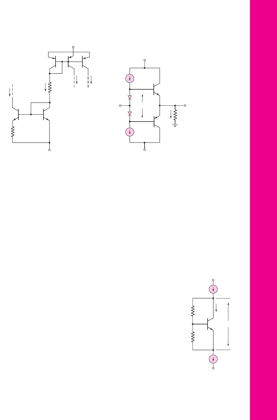
Section 13.2 A Bipolar Operational Amplifier Circuit
13.6 Consider the input stage of the 741 op-amp in Figure 13.4(b). (a) Assume
the input voltages are
V
1
= 0
and
V
2
=+15
V. Consider the B–E voltage
of each transistor and determine which transistor acts as the protection
device. (b) Repeat part (a) for
V
1
=−15 V
and
V
2
= 0
.
13.7 For the input stage of the 741 op-amp, assume B–E breakdown voltages of
5 V for the npn devices and 50 V for the pnp devices. Estimate the differen-
tial input voltage at which breakdown will occur.
13.8 Consider the bias circuit portion of the 741 op-amp in Figure 13.5. Assume
transistor parameters of
I
S
= 5 ×10
−16
A. Neglect base currents. (a) Re-
design the circuit such that
I
REF
= 0.5
mA and
I
C10
= 30 μ
A for bias volt-
ages of
±15
V. What are the values of
V
BE11
,
V
EB12
, and
V
BE10
? (b) Using
the resistor values found in part (a) and assuming
V
BE
(on) = V
EB
(on) =
0.6
V, determine the values of
I
REF
and
I
C10
. (c) What are the percent dif-
ferences in the current values between parts (a) and (b).
13.9 Repeat Problem 13.8 for bias voltages of
±5
V.
13.10 Consider the bias circuit shown in Figure P13.10. Let
V
+
= 3
V,
V
−
=−3
V,
R
1
= 80 k
, and
R
E
= 3.5k
. Assume transistor parame-
ters of
I
S
= 5 ×10
−15
A for
Q
1
,
Q
2
,
Q
3
;
I
S
= 3 ×10
−15
A for
Q
4
; and
I
S
= 10
−15
A for
Q
5
. (a) Find the currents
I
REF
,
I
3
,
I
4
, and
I
5
. (b) Repeat
part (a) for
I
S
= 8 ×10
−15
A for
Q
4
and
I
S
= 2 ×10
−15
A for
Q
5
.
13.11 The minimum recommended supply voltages for the 741 op-amp are
V
+
= 5
V and
V
−
=−5V
. Using these lower supply voltages, calculate:
I
REF
, I
C10
, I
C6
, I
C17
, and
I
C13A
.
13.12 An expanded circuit diagram of the 741 input stage is shown in Figure 13.6.
Assume
I
C10
= 50 μ
A. If the current gain of the npn transistors is
β
n
= 90
nea80644_ch13_947-1008.qxd 6/23/09 1:59 PM Page 998 pmath DATA-DISK:Desktop Folder:23/06/09:MHDQ134-13:
Chapter 13 Operational Amplifier Circuits 999
V
+
Q
5
Q
4
Q
2
V
–
R
1
R
E
Q
3
Q
1
I
5
I
4
I
REF
I
3
Figure P13.10
and the current gain of the pnp transistors is
β
p
= 40
, determine
I
C9
,
I
C2
,
I
C4
,
I
B9
, and
I
B4
. Do not neglect npn transistor base currents.
13.13 Consider the 741 op-amp in Figure 13.3, biased with
V
+
= 15 V
and
V
−
=−15 V
. Assume that no load is connected at the output, and let the
input voltages be zero. Calculate the total power dissipated in the op-amp
circuit. What are the currents supplied by
V
+
and
V
−
?
13.14 Consider the 741 circuit in Figure 13.3. (a) Determine the maximum range
of common-mode input voltage if the bias voltages are
±15
V. (b) Repeat
part (a) if the bias voltages are
±5
V.
13.15 Consider the output stage of the 741 op-amp shown in Figure 13.8. As-
sume
v
1
= v
2
= 0
at the input and assume the bias voltages are
V
+
= 5
V
and
V
−
=−5
V. Let
I
REF
= 0.5
mA. All other circuit and transistor para-
meters are described in Example 13.3. Find
I
C13A
,
I
R10
,
I
C19
,
I
C18
,
V
BE19
,
V
BE18
, and
I
C14
.
*13.16 Consider the output stage in Figure P13.16 with parameters
V
+
= 5
V,
V
−
=−5
V,
R
L
= 10 k
, and
I
Bias
= 80 μ
A. Assume the diode parameters
are
I
SD
= 5 ×10
−15
A, and assume the transistor parameters are
I
SQ
=
8 × 10
−15
A and
β
n
= β
p
= 120
. (a) For
v
I
= 0
, determine
V
BB
,
I
CN
, and
I
CP
. (b) For
v
I
= 3
V, determine
v
O
,
i
L
,
V
BB
,
I
CN
, and
I
CP
.
D13.17 Figure P13.17 shows a circuit often used to provide the
V
BB
voltage in the
op-amp output stage. Assume
I
S
= 5 ×10
−15
A for the transistor,
I
Bias
=
120 μ
A, and
I
C
= 0.9I
Bias
. Neglect the base current. Design the circuit such
that
V
BB
= 1.160
V.
13.18 Assume bias voltages on the 741 op-amp of
±15
V. (a) Determine the
differential-mode voltage gain of the first stage if
R
1
= R
2
= 0
. (b) Deter-
mine the voltage gain of the second stage if
R
8
= 0
.
13.19 Recalculate the voltage gain of the 741 op-amp input stage if
I
C10
= 40 μA
.
*13.20 Assume the 741 op-amp shown in Figure 13.3 is biased at
±5
V. Using the
circuit parameters given in the figure and transistor parameters given in
D
2
D
1
V
+
V
–
I
Bias
I
Bias
v
O
v
I
R
L
Q
P
Q
N
V
BB
+
–
i
L
Figure P13.16
V
+
V
–
I
Bias
I
Bias
R
2
R
1
V
BB
+
–
I
C
Q
Figure P13.17
nea80644_ch13_947-1008.qxd 6/23/09 1:59 PM Page 999 pmath DATA-DISK:Desktop Folder:23/06/09:MHDQ134-13:

1000 Part 2 Analog Electronics
Examples 13.1 through 13.5, calculate the overall small-signal voltage gain
of the amplifier.
*13.21 Repeat Problem 13.20 assuming Early voltages of 100 V.
13.22 Consider the output stage of the 741 op-amp shown in Figure 13.8. Assume
I
Bias
= 0.18
mA and assume transistor parameters of
I
S
= 10
−14
A and
β
n
= 200
. (a) Determine the value of
R
10
that would result in
I
C18
=
0.25I
C19
. (b) What are the resulting voltages
V
BE18
and
V
BE19
?
13.23 The basic bias circuit of the output transistors of the 741 op-amp is shown
in Figure P13.23. (a) Sketch the small-signal equivalent circuit. (b) Assum-
ing
V
A
= 50
V and using the parameters described in Example 13.3, deter-
mine the equivalent small-signal resistance
R
eq
= v
x
/i
x
.
13.24 Calculate the output resistance of the 741 op-amp if Q
14
is conducting and
Q
20
is cut off. Assume an output current of 2 mA.
13.25 (a) Determine the differential input resistance of the 741 op-amp when
biased at
±15
V. (b) Repeat part (a) when the op-amp is biased at
±5
V.
13.26 The frequency response of a particular 741 op-amp shows that the op-
amp has a phase margin of 70 degrees. If a second single pole exists, in
addition to the dominant pole, determine the frequency of the second
pole. Use the overall gain and dominant-pole parameters calculated in
Section 13.2.
13.27 An op-amp that is internally compensated by Miller compensation has a
unity-gain bandwidth of 10 MHz and a low-frequency gain of
10
6
. (a) What
is the dominant pole frequency? (b) The feedback capacitor is across the
second stage, which has a gain of
−10
3
. The effective resistance at the input
of the second stage is
R
eq
= 1.2M
. What is the value of the feedback
capacitor?
13.28 A three-stage 741 op-amp has a low-frequency open-loop gain of 200,000
and a dominant pole frequency of 10 Hz. The second and third poles are at
the same frequency. If the phase margin is 70 degrees, determine the fre-
quency of the second and third poles.
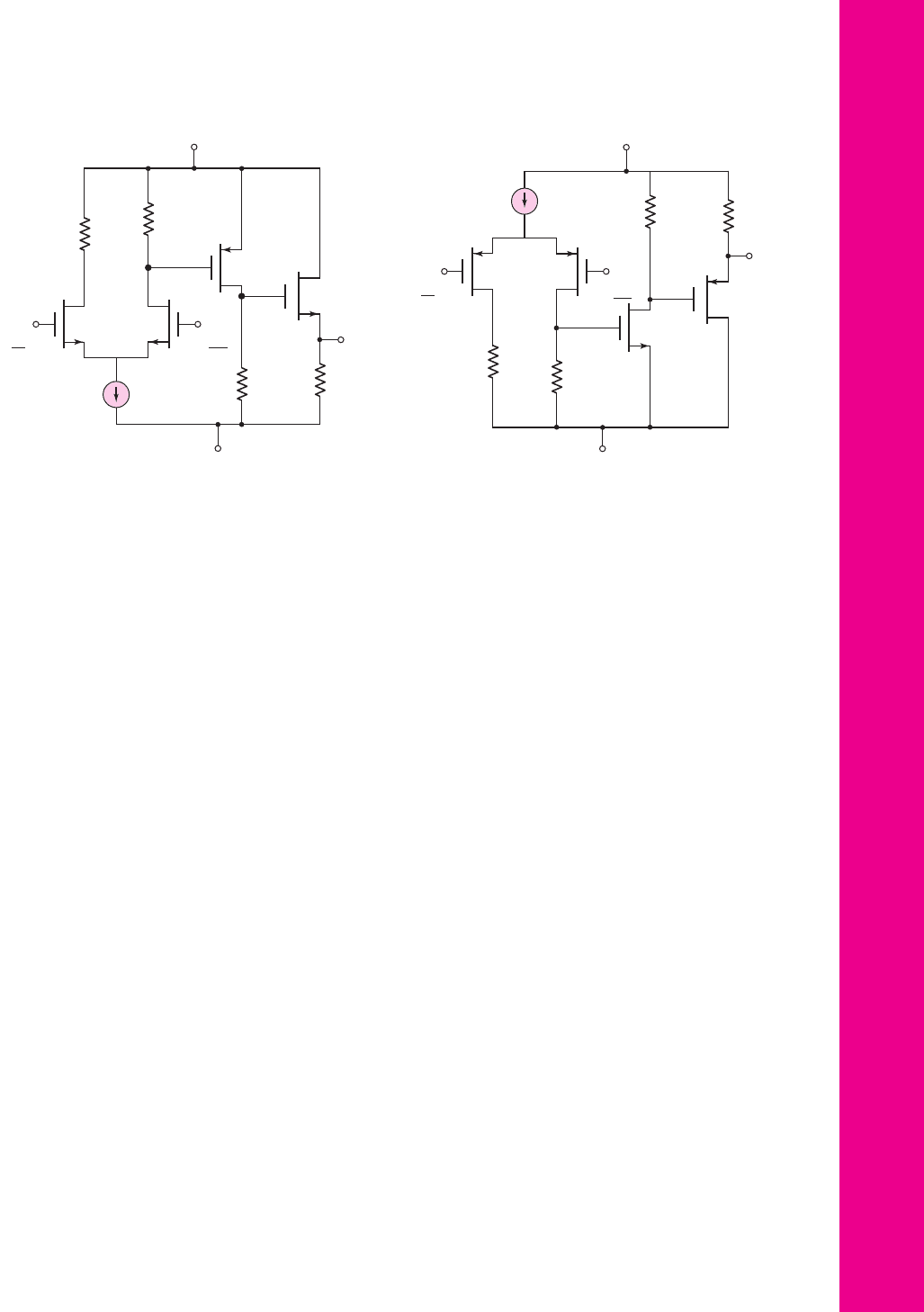
Section 13.3 CMOS Operational Amplifier Circuits
13.29 Consider the simple CMOS op-amp circuit in Figure P13.29 biased with
I
Q
= 200 μ
A. The transistor parameters are
k
n
= 100 μ
A/V
2
,
k
p
=
40 μ
A/V
2
,
V
TN
= 0.4
V,
V
TP
=−0.4
V, and
λ
n
= λ
p
= 0
. The transistor
width-to-length ratios are
(W/L)
1,2
= 20
,
(W/L)
3
= 50
, and
(W/L)
4
= 40
.
(a) Design the circuit such that
I
D3
= 150 μ
A,
I
D4
= 200 μ
A, and
v
o
= 0
for
v
1
= v
2
= 0
. (b) Find the small-signal voltage gains (i)
A
d
= v
o1
/v
d
,
(ii)
A
2
= v
o2
/v
o1
, and (iii)
A
3
= v
o
/v
o2
. (c) Determine the overall small-
signal voltage gain
A = v
o
/v
d
.
13.30 A simple CMOS op-amp circuit is shown in Figure P13.30 with
I
Q
=
100 μ
A. The transistor parameters are the same as given in Problem
13.29 except for the width-to-length ratios. The width-to-length ratios are
(W/L)
1,2
= 80
,
(W/L)
3
= 25
, and
(W/L)
4
= 100
. (a) The circuit is to be
designed such that
I
DQ3
= 100 μ
A,
I
DQ4
= 200 μ
A, and
v
o
= 0
for
v
1
= v
2
= 0
. (b) Determine the small-signal voltage gains (i)
A
d
= v
o1
/v
d
,
(ii)
A
2
= v
o2
/v
o1
, and (iii)
A
3
= v
o
/v
o2
. (c) Find the overall small-signal
voltage gain
A = v
o
/v
d
.
v
x
Q
18
Q
19
R
10
=
50 kΩ
+
–
i
x
Figure P13.23
nea80644_ch13_947-1008.qxd 6/23/09 1:59 PM Page 1000 pmath DATA-DISK:Desktop Folder:23/06/09:MHDQ134-13:
D13.31 Consider the MC14573 op-amp in Figure 13.14. The dc bias currents and
small-signal voltage gains were determined in Examples 13.8 and 13.9.
Redesign the circuit such that the width-to-length ratio of M
1
and M
2
is
increased from 12.5 to 50. All other circuit and transistor parameters remain
the same. (a) Determine the original transconductance of M
1
and M
2
, and
the new transconductance value. (b) Determine the new values of voltage
gain for the input and second stages, and the overall voltage gain.
13.32 Consider the basic diff-amp with active load and current biasing in Fig-
ure 13.14. Using the parameters and results of Example 13.8, determine
the maximum range of common-mode input voltage under the conditions
that the minimum source-to-drain voltage for a PMOS is limited to
v
SD
(min) = v
SD
(sat) + 0.2
V and the minimum drain-to-source voltage for
an NMOS is limited to
v
DS
(min) = v
DS
(sat) + 0.2
V.
13.33 The CMOS op-amp in Figure 13.14 is biased at
V
+
= 5
V and
V
−
=
−5
V. Let
R
set
= 50 k
. Assume transistor parameters of
V
TN
= 0.7
V,
V
TP
=−0.7
V,
k
n
= 100 μ
A/V
2
,
k
p
= 40 μ
A/V
2
,
λ
n
= 0.02 V
−1
, and
λ
p
= 0.04 V
−1
. The transistor width-to-length ratios are
(W/L)
3,4
= 15
,
(W/L)
7
= 30
, and
(W/L) = 50
for all other transistors. (a) Determine
I
set
,
I
Q
, and
I
DQ7
. (b) Find the small-signal voltage gains of the input and sec-
ond stages, and the overall voltage gain.
13.34 For the CMOS op-amp in Figure 13.14, the dc biasing is designed such that
I
set
= I
Q
= I
DQ8
= 200 μ
A. The transistor parameters are
V
TN
= 0.5
V,
V
TP
=−0.5
V,
k
n
= 100 μ
A/V
2
,
k
p
= 40 μ
A/V
2
,
λ
n
= 0.015 V
−1
, and
λ
p
= 0.025 V
−1
. The transistor width-to-length ratios are
(W/L)
1,2
= 50
,
(W/L)
3,4
= 15
,
(W/L)
5,6,8
= 10
, and
(W/L)
7
= 30
. Determine the small-
signal voltage gains of the input and second stages, and the overall volt-
age gain.
13.35 Consider the MC14573 op-amp in Figure 13.14, with circuit and transistor
parameters as given in Examples 13.8 and 13.9. If the compensation capac-
itor is
C
1
= 12
pF, determine the dominant-pole frequency.
Chapter 13 Operational Amplifier Circuits 1001
R
D1
R
D2
R
D1
v
o
v
o1
I
Q
M
1
M
2
M
3
M
4
R
S
V
+
= 3 V
V
–
= –3 V
v
2
=
v
2
–v
d
2
v
1
=
v
d
2
Figure P13.29
V
–
= –3 V
V
+
= 3 V
M
1
M
2
R
D3
M
3
M
4
v
2
=
–v
d
2
v
1
=
v
d
2
v
o1
v
o2
R
D1
R
D1
I
Q
v
o
R
S
Figure P13.30
nea80644_ch13_947-1008.qxd 6/23/09 1:59 PM Page 1001 pmath DATA-DISK:Desktop Folder:23/06/09:MHDQ134-13:

13.36 The CMOS op-amp in Figure 13.14 has circuit and transistor parameters as
given in Problem 13.33. Determine the compensation capacitor required
such that the dominant-pole frequency is
f
PD
= 8
Hz.
13.37 Consider the CMOS op-amp in Figure 13.14, with transistor and circuit
parameters as given in Examples 13.8 and 13.9. Determine the output resis-
tance R
o
of the open-loop circuit.
13.38 A simple output stage for an NMOS op-amp is shown in Figure P13.38.
Device
M
1
operates as a source follower. The bias voltages are
V
+
= 3
V
and
V
−
=−3
V. Transistor parameters are
k
n
= 100 μ
A/V
2
,
V
TN
=
0.4
V, and
λ = 0.025 V
−1
. Assume that transistors
M
2
–
M
5
are matched.
(a) Determine the width-to-length ratios of transistors
M
2
–
M
5
such that
I
DQ2
= 0.5
mA. (b) Determine the
W/L
ratio of
M
1
such that the voltage
gain is 0.98. (c) If the output resistance of source
v
I
is 10 k
, determine the
output resistance of this output stage.
1002 Part 2 Analog Electronics
V
+
V
–
M
1
M
2
M
5
M
4
M
3
v
O
v
I
Figure P13.38
M
5
M
8P
M
8N
M
9
V
GS9
= 1.1737 V
M
6
M
7
v
o
v
G9
v
G5
I
Q2
+
–
V
SG5
= 1.035 V
+
–
–5 V
+5 V
20
1
50
1
25
1
80
1
Figure P13.39
13.39 The circuit in Figure P13.39 is another form of an output stage for the CMOS
op-amp shown in Figure 13.15. Assume the same transistor parameters as
given in Example 13.10. The width-to-length values of some transistors are
given and the applied gate-to-source voltages of M
5
and M
9
are shown.
(a) What is the bias current I
Q2
? (b) Determine the W/L ratios of M
8P
and
M
8N
such that the quiescent currents in M
6
and M
7
are
25 μA
.
D13.40 Consider the three-stage CMOS op-amp in Figure 13.15. Design an all-
NMOS transistor current source circuit to establish
I
Q1
= 150 μ
A. The
NMOS transistor parameters are
k
n
= 100 μ
A/V
2
and
V
TN
= 0.5
V.
Assume the minimum width-to-length ratio of any transistor is 2. Assume
(W/L)
10
= (W/L)
11
= 20
as shown in the figure.
nea80644_ch13_947-1008.qxd 6/23/09 1:59 PM Page 1002 pmath DATA-DISK:Desktop Folder:23/06/09:MHDQ134-13:

13.41 Assume
I
REF
= 250 μA
and
(W/L)
8
= 5
in the CMOS op-amp shown in
Figure 13.15. Determine (a) the quiescent currents in M
6
and M
7
and
(b) the overall small-signal voltage gain. Assume transistor parameters as
given in Example 13.10.
*13.42 The CMOS folded cascode circuit in Figure 13.17 is biased at
±5
V and
the reference current is
I
REF
= 50 μA
. The transistor parameters are
V
TN
=
0.5 V,
V
TP
=−0.5V
,
K
n
= K
p
= 0.5mA/V
2
, and
λ
n
= λ
p
=
0.015 V
−1
. (a) Determine the small-signal differential voltage gain.
(b) Find the output resistance of the circuit. (c) If the capacitance at the out-
put node is
C
L
= 5
pF, determine the unity-gain bandwidth of the amplifier.
*D13.43 The CMOS folded cascode amplifier in Figure 13.17 is to be redesigned to
provide a differential voltage gain of 10,000. The biasing is the same as
described in Problem 13.42. The transistor parameters are
V
TN
= 0.5V
,
V
TP
=−0.5V
,
k
n
= 80 μA/V
2
,
k
p
= 35 μA/V
2
,
λ
n
= 0.015 V
−1
, and
λ
p
= 0.02 V
−1
. Assume
(W/L)
p
= 2.2(W/L)
n
where appropriate so that
the electrical parameters of PMOS and NMOS devices are nearly identical.
*D13.44 The CMOS folded cascode amplifier of Figure 13.17 is to be designed to
provide a differential voltage gain of 25,000. The maximum power dissi-
pated in the circuit is to be limited to 3 mW. Assume transistor parameters
as described in Problem 13.43, except the relation between NMOS and
PMOS width-to-length ratios need not be maintained.
13.45 The bias current in the CMOS current-gain op-amp in Figure 13.18 is
I
Q
= 120 μ
A. The transistor parameters are
V
TN
= 0.5
V,
V
TP
=−0.5
V,
k
n
= 100 μ
A/V
2
,
k
p
= 40 μ
A/V
2
,
λ
n
= 0.02
V
−1
, and
λ
p
= 0.04
V
−1
.
The transistor width-to-length ratios are 20 except for
M
5
and
M
6
. Let
B = 3
. (a) Determine the small-signal differential voltage gain. (b) Find
the output resistance of the circuit. (c) If the total capacitance at the output
terminal is 5 pF, determine the dominant-pole frequency and the unity-gain
bandwidth.
D13.46 The CMOS current gain op-amp in Figure 13.18 is to be redesigned to
provide a differential voltage gain of 400. The transistor parameters are
V
TN
= 0.5V
,
V
TP
=−0.5V
,
k
n
= 80 μA/V
2
,
k
p
= 35 μA/V
2
,
λ
n
=
0.015 V
−1
, and
λ
p
= 0.02 V
−1
. The bias current is to be
I
Q
= 80 μA
. Let
B = 2.5
. (a) Design the basic amplifier to provide the specified voltage
gain. (b) Design a current source to provide the necessary bias current.
(c) Determine the unity-gain bandwidth if the capacitance at the output
terminal is 3 pF.
D13.47 Redesign the CMOS cascode current mirror in Figure 13.19 to provide a
differential voltage gain of 20,000. The bias current and transistor para-
meters are the same as in Problem 13.46. (a) Design the basic amplifier to
provide the specified voltage gain. (b) Design a current source to provide
the necessary bias current. (c) Determine the unity gain bandwidth if the
capacitance at the output terminal is 3 pF.
Section 13.4 BiCMOS Operational Amplifier Circuits
13.48 A simple BiCMOS amplifier is shown in Figure P13.48. The MOS transistor
parameters are
k
p
= 40 μ
A/V
2
,
V
TP
=−0.4
V,
λ = 0
, and
(W/L)
1,2
= 50
,
and the bipolar transistor parameters are
V
BE
(on) = 0.7
V,
β = 120
, and
V
A
=∞
. (a) Design the circuit such that
I
CQ
= 300 μ
Aand
v
o
= 0
for
Chapter 13 Operational Amplifier Circuits 1003
nea80644_ch13_947-1008.qxd 6/23/09 1:59 PM Page 1003 pmath DATA-DISK:Desktop Folder:23/06/09:MHDQ134-13:
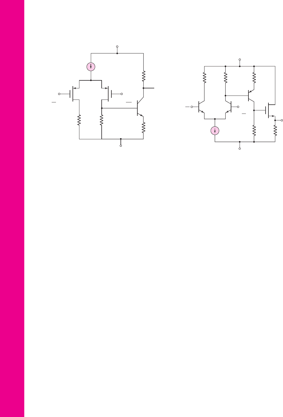
v
1
= v
2
= 0
. (b) Determine the small-signal differential voltage gain of the
first stage
A
d
= v
o1
/v
d
. (c) Find the small-signal voltage gain of the second
stage
A
2
= v
o
/v
o1
. (d) Determine the overall small-signal voltage gain
A = v
o
/v
d
.
13.49 Consider the simple BiCMOS amplifier shown in Figure P13.49. The bipo-
lar transistor parameters are
β
n
= β
p
= 120
,
V
BE
(on) = V
EB
(on) = 0.7
V,
V
A
=∞
, and the MOS transistor parameters are
V
TN
= 0.4
V,
K
n
=
3
mA/V
2
,
λ = 0
. (a) Design the circuit such that
I
CQ3
= I
DQ1
= 300 μ
A
and
v
o
= 0
for
v
1
= v
2
= 0
. (b) Determine the small-signal voltage gain of
the first stage
A
d
= v
o1
/v
d
. (c) Find the small-signal voltage gain of the
second stage
A
2
= v
o2
/v
o1
. (d) Determine the small-signal voltage gain of
the third stage
A
3
= v
o
/v
o2
. (e) Find the overall differential voltage gain
A = v
o
/v
d
.
13.50 A BiCMOS amplifier is shown in Figure P13.50. The transistor parameters
are
V
TP
=−0.4
V,
k
p
= 40 μ
A/V
2
,
W/L = 40
,
λ = 0.035
V
−1
,
β = 120
,
and
V
A
= 150
V. The bias current is
I
Q
= 250 μ
A. (a) Determine the
small-signal parameters of the transistors. (b) Find the small-signal differ-
ential voltage gain.
13.51 Design a BiCMOS amplifier that is complementary to the one in Figure
P13.50 in that the input devices are NMOS and the load transistors are
pnp. Assume transistor parameters of
V
TN
= 0.4
V,
k
n
= 100 μ
A/V
2
,
W/L = 40
,
λ = 0.02
V
−1
,
β = 80
, and
V
A
= 100
V. Assume the bias cur-
rent is
I
Q
= 250 μ
A. (a) Determine the small-signal parameters of the
transistors. (b) Find the small-signal differential voltage gain.
*13.52 The reference current in the BiCMOS folded cascode amplifier in Fig-
ure 13.20 is
I
REF
= 200 μA
and the circuit bias voltages are
±10
V. The
MOS transistor parameters are the same as in Problem 13.42. The BJT
parameters are
β = 120
and
V
A
= 80
V. (a) Determine the small-signal
differential voltage gain. (b) Find the output resistance of the circuit. (c) If
1004 Part 2 Analog Electronics
Figure P13.49
Figure P13.48
V
–
= –3 V
M
1
M
2
R
C
R
E
=
0.4 kΩ
R
D
R
D
I
Q
= 300 mΑ
v
1
=
v
d
2
v
2
=
v
o1
–v
d
2
v
o
V
+
= 3 V
V
–
= –3 V
V
+
= 3 V
R
E
=
0.5 kΩ
R
C2
R
C1
R
C1
Q
1
Q
2
R
S
Q
3
I
Q
=
500 mA
v
o1
v
o2
v
o
v
1
=
v
d
2
v
2
=
–v
d
2
M
1
nea80644_ch13_947-1008.qxd 6/23/09 1:59 PM Page 1004 pmath DATA-DISK:Desktop Folder:23/06/09:MHDQ134-13:

Chapter 13 Operational Amplifier Circuits 1005
the capacitance at the output node is 5 pF, determine the unity-gain band-
width of the amplifier.
*D13.53 The BiCMOS folded cascode amplifier in Figure 13.20 is to be designed to
provide a differential voltage gain of 25,000. The maximum power dissipated
in the circuit is to be limited to 10 mW. Assume MOS transistor parameters
as described in Problem 13.43. The BJT parameters are
β = 120
and
V
A
= 80
V.
13.54 If the CA3140 op-amp is biased at
V
+
= 15
V and
V
−
=−15 V
, deter-
mine the input common-mode voltage range. Assume B–E voltages of
0.6 V for the bipolar transistors and
|V
TP
|=1.4V
for the MOSFETs.
13.55 Consider the bias circuit portion of the CA3140 op-amp in Figure
13.22. If
V
BE7
= 0.6
V for
Q
7
and
V
TP
=−1.0
V for
M
8
, determine
the required value of the conduction parameter for
M
8
such that
I
1
= I
2
= 150 μ
A.
13.56 In the bias portion of the CA1340 op-amp in Figure 13.22, the bipolar
transistor parameters are
V
BE
(npn) = 0.6
V and
V
EB
(pnp) = 0.6
V
and the MOSFET parameters are
V
TP
=−1.2
V and
K
p
= 0.15
mA/V
2
.
(a) Determine the currents
I
1
= I
2
. (b) If the bias voltages are
V
+
=−V
−
≡ V
S
, determine the minimum value of
V
S
such that the bias
currents are independent of the supply voltage.
13.57 Consider the CA3140 op-amp in Figure 13.21. If the bias currents change
such that
I
C5
= I
C4
= 300 μA
, determine the voltage gains of the input
and second stages, and find the overall voltage gain.
13.58 Assume the gain stage of the CA3140 op-amp is modified to include an
emitter resistor, as shown in Figure 13.23. Let
λ = 0.02 V
−1
for M
10
. If
the transistor bias currents in M
10
and Q
12
are
150 μA
and the current in
Q
13
is
300 μA
, determine the dominant-pole frequency and unity-gain
bandwidth.
V
+
V
+
V
–
M
1
M
2
I
Q
Q
1
Q
2
Q
3
v
o
v
1
v
2
Figure P13.50
nea80644_ch13_947-1008.qxd 6/23/09 1:59 PM Page 1005 pmath DATA-DISK:Desktop Folder:23/06/09:MHDQ134-13:
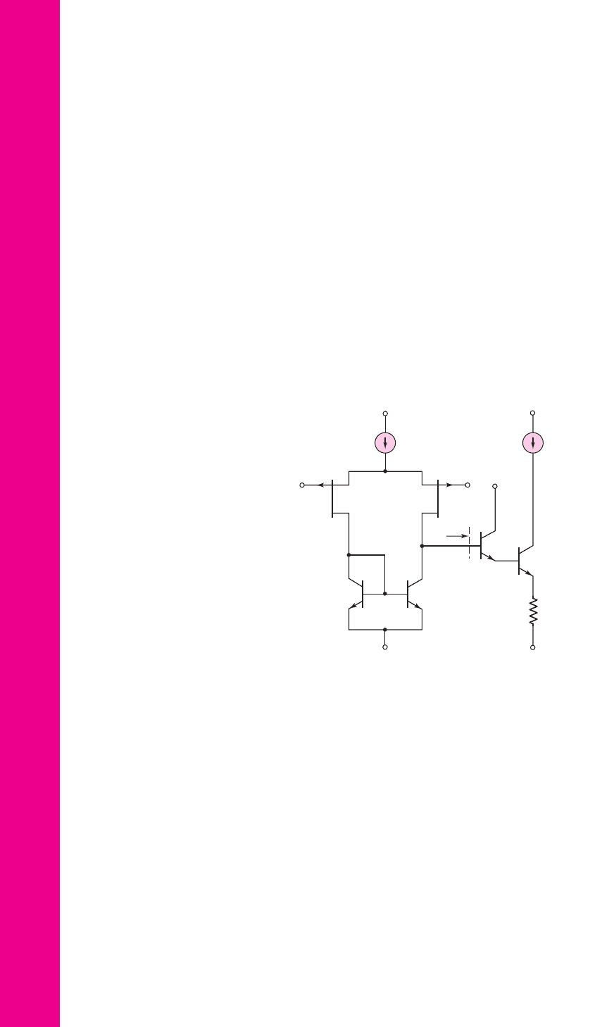
Section 13.5 JFET Operational Amplifier Circuits
13.59 In the LF155 BiFET op-amp in Figure 13.25, the combination of Q
3
, J
6
, and
Q
4
establishes the reference bias current. Assume the power supply voltages
are
V
+
= 10
V and
V
−
=−10 V
. The transistor parameters are
V
EB
(on) =
0.6V
,
V
BE
(on) = 0.6V
, and
V
P
= 4
V for Q
3
, Q
4
, and J
6
, respectively.
Determine the required I
DSS
value for J
6
to establish a reference current of
I
REF
= 0.8mA
.
13.60 Consider the circuit in Figure P13.60. A JFET diff-amp input stage drives a
bipolar Darlington second stage. The p-channel differential pair J
1
and J
2
are connected to the bipolar active load transistors Q
3
and Q
4
. Assume JFET
parameters of
V
P
= 3
V,
I
DSS
= 200 μA
, and
λ = 0.02 V
−1
. The bipolar
transistor parameters are
β = 100
and
V
A
= 50
V. (a) Determine the input
resistance R
i2
to the second stage. (b) Calculate the small-signal differential-
mode voltage gain of the input stage. Compare this value to the 741 and
CA3140 input stage results.
1006 Part 2 Analog Electronics
R
E
= 0.3 kΩ
V
+
V
–
V
–
V
+
V
+
I
Q
= 200 mA
I
Q
= 200 mA
Q
5
Q
4
Q
3
Q
6
J
2
J
1
v
2
v
1
R
i2
Figure P13.60
D13.61 Consider the BiFET differential input stage in Figure P13.61, biased with
power supply voltages
V
+
and
V
−
. Let
V
+
=−V
−
≡ V
S
. (a) Design the
bias circuit such that
I
REF2
= 100 μA
for supply voltages in the range
3 ≤ V
S
≤ 12 V
. Determine V
ZK
, R
3
, and the JFET parameters. (b) Deter-
mine the value of R
4
such that
I
O1
= 500 μA
when
V
+
= 12 V
.
13.62 The BiFET diff-amp input stage in Figure P13.61 is biased at
I
O1
= 1
mA.
The JFET parameters are
V
P
= 4
V,
I
DSS
= 1
mA, and
λ = 0.02 V
−1
. The
bipolar transistor parameters are
β = 200
and
V
A
= 100
V. (a) For
R
1
= R
2
= 500
, determine the minimum load resistance R
L
such that a
differential-mode voltage gain of
A
d
= 500
is obtained in the input stage.
(b) If
R
L
= 500 k
, determine the range of resistance values
R
1
= R
2
such
that a differential-mode voltage gain of
A
d
= 700
is obtained in this input
stage.
nea80644_ch13_947-1008.qxd 6/23/09 1:59 PM Page 1006 pmath DATA-DISK:Desktop Folder:23/06/09:MHDQ134-13:
COMPUTER SIMULATION PROBLEMS
Consider the input stage and bias circuit of the 741 op-amp in Figure 13.5.
Transistor Q
10
may be replaced by a constant-current source equal to
19 μA
. Assume: the npn devices have parameters
β = 200
and
V
A
=
150
V; the pnp devices have parameters
β = 50
and
V
A
= 50
V; and all tran-
sistors have
I
S
= 10
−14
A
. Place an appropriate ac load at the collector of
Q
6
. (a) Using a computer simulation, determine the differential voltage
gain of the input stage. (b) Determine the differential-mode input resis-
tance. (c) Determine the common-mode input resistance.
13.64 The output stage of the 741 op-amp is shown in Figure 13.9. Transistor
Q
13
may be replaced with a constant-current source equal to 0.18 mA.
Use standard transistors. (a) Using a computer simulation, plot the voltage
transfer function
v
o
versus
v
13
. What is the voltage gain? Has the
crossover distortion been eliminated? (b) Apply an input voltage
v
13
that
establishes an output voltage of
v
o
= 5
V. Then set
R
L
= 0
. Find the out-
put short-circuit current and the transistor currents.
13.65 Consider the BiCMOS input stage of the CA3140 op-amp in Figure 13.21.
Transistor Q
5
can be replaced with a constant-current source of
200 μA
.
Assume: bipolar transistor parameters of
β = 200
,
I
EO
= 10
−14
A
, and
V
A
=
50 V; and MOSFET parameters of
K
p
= 0.6
mA/V
2
,
|V
TP
|=1V
,
and
λ = 0.01 V
−1
. Using an appropriate ac load at the collector of Q
12
,
determine the differential gain of the input stage. Compare the computer
analysis results with those in Example 13.12.
13.66 Consider the CMOS op-amp in Figure 13.14. Assume the circuit and tran-
sistor parameters are as given in Example 13.8. In addition, let
λ =
Chapter 13 Operational Amplifier Circuits 1007
R
2
R
1
Q
C
v
–
v
+
R
4
I
o1
R
3
I
REF1
R
load
i
out
v
out
I
REF2
I
D2
I
C4
I
D1
I
C3
I
o2
I
R1
≅
I
CA
D
2
D
1
Bias for
Zener D
2
Q
D
Q
A
Q
3
Q
4
Q
1
Q
2
Q
E
V
–
pnp
current
mirror
JFET
input
pair
Incremental
current
mirror
Q
B
+
–
V
D1
+
–
V
ZK
+
–
I
o1
2
Bias
for Q
A
Figure P13.61
nea80644_ch13_947-1008.qxd 6/23/09 1:59 PM Page 1007 pmath DATA-DISK:Desktop Folder:23/06/09:MHDQ134-13:
13.63